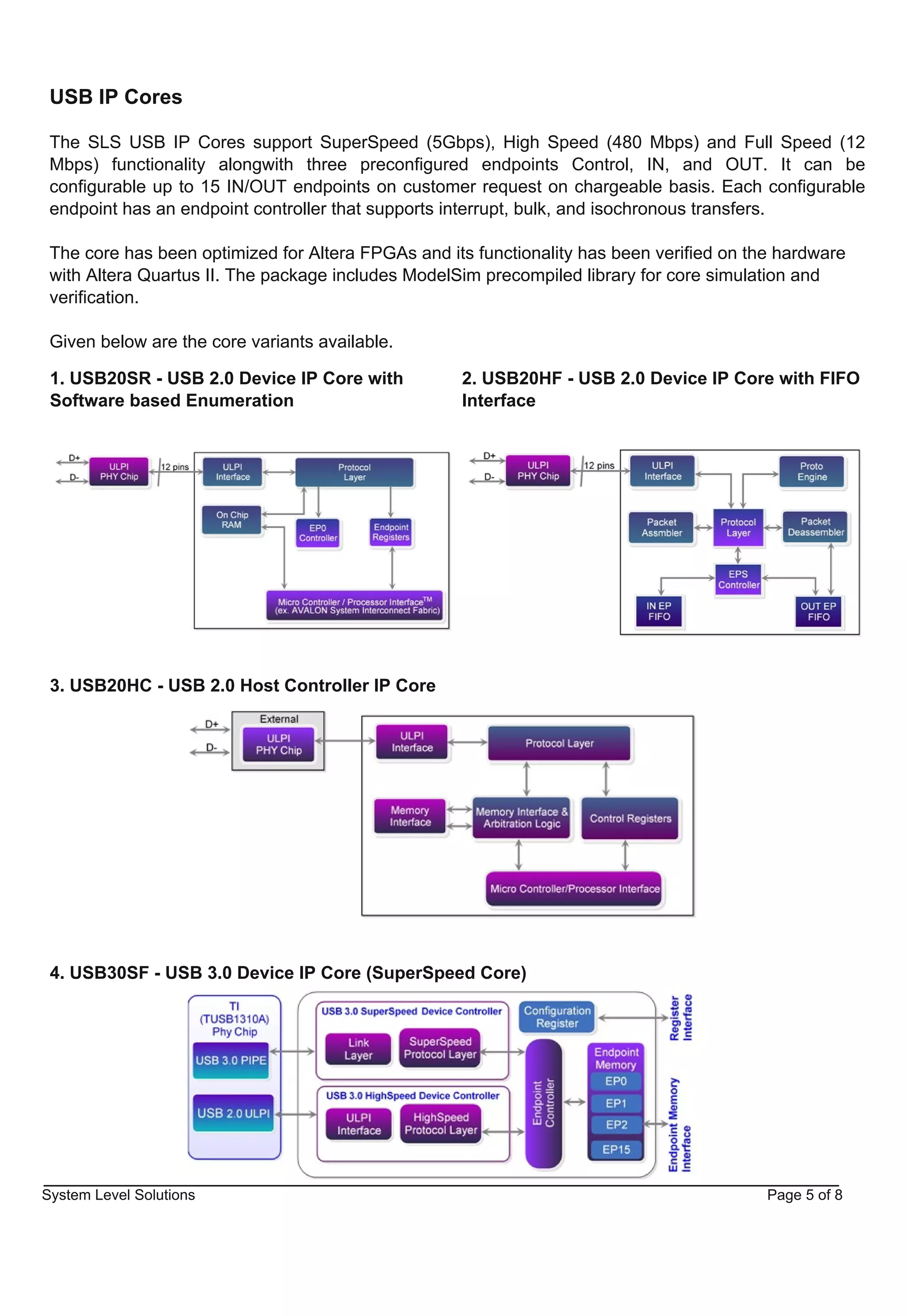
SUPERSPEED USB and NAND
 FLASH DESIGNS                                                           Whitepaper


Date: June 19. 2012                                                                             Version: 1.0


There is a trend observed in the market for designing products with SuperSpeed USB and NAND Flash inside.
There are camera manufacturers, printer manufacturers as well as FLASH drive manufacturers involved in the
trend. It is crucial, at this point of time in the market, to have a proper know­how on what factors affect such
designs and what can be done to achieve a successful and a long­life design. The paper focuses on providing
information base required for proceeding with the design and what factors would affect such designs.


USB is one of the most successful peripheral that has penetrated heavily into CE and mobile
systems. The USB standard is developed by The USB Implementers Forum. The increasing need
for higher speeds led to the development of more standards which has led to SuperSpeed USB. The
USB­IF has put up a video on Vimeo for SuperSpeed USB.                     It can be viewed at:
http://vimeo.com/20616954

SuperSpeed USB features as listed on usb.org are given below:


     SuperSpeed USB is a Sync­N­Go technology that minimizes user wait­time.
     SuperSpeed USB will provide Optimized Power Efficiency.No device polling and lower active
     and idle power requirements.
     SuperSpeed USB is backwards compatible with USB 2.0. Devices interoperate with USB 2.0
     platforms. Hosts support USB 2.0 legacy devices.


The USB 3.0 standard claims that it is 10 times faster than USB 2.0. The theoretical speed is
4.8Gbps (600MBps). However looking at various realistic speed test reports made available by more
than one developers, it has been concluded that 400MBps is the maximum achievable speed for this
standard.

The core efficiency is dependent on a number of factors like 8b/10b encoding, packet structure and
framing, link level flow control and protocol overhead.

At 5Gbps signalling rate with 8b/10b encoding, the raw throughput is 500MBps. When link flow
control, packet framing, and protocol overhead are considered, it is realistic for 400MBps or more to
be delivered to an application.

In an idealized system, as leading experts say, the controllers and PHYs can achieve SuperSpeed
USB 3.0 speeds of 400 Megabytes per second (or 4 Gigabits per second).
System Level Solutions                                                                               Page 1 of 8
WHAT IS NAND FLASH?
NAND Flash is a non­volatile memory chip used for storage generally in flash drives, SD Cards, SSDs
etc. The standard is developed by ONFI (Open NAND Flash Interface), which is a workgroup
consisting of multiple companies and involved in designing, enabling and simplifying the integration of
the NAND Flash into various electronic products.

NAND Flash devices can be found in different variants and can be selected depending on the cost,
size and usage model. Some NAND Flash memories are slower and cheaper, while some are faster
and quite expensive. Therefore, a NAND Flash used in a Flash drive will be different than the one
used in an ultrabook!


WHAT AFFECTS THE PERFORMANCE?
Depending on the NAND Flash used in the system, the performance can be estimated. But, there are
a number of factors affecting the speed and performance of USB in a system. Eric Huang has listed
the dependencies very interestingly in his blog. I am listing them here.

The USB transfer speed is affected by the following factors:

      Number of applications running on the host machine
      The speed of the application itself
      The quality of the drivers (host as well as device)
      The bus on the hardware that moves data from USB controller to CPU (on host as well as device
      side)
      The USB PHY
      The USB Cable


A NON-IDEALIZED SYSTEM
Looking into a non­idealized system, the SLS SuperSpeed USB Device IP Core tests performed on
GigaByte A75 Motherboard have indicated the performance ~2.1Gigabits per second (262.5
Megabytes per second) with mass storage interface and ~2.7Gigabits per second (337.5
Megabytes per second) with raw interface.

About SLS SuperSpeed USB Device IP Core
The SLS SuperSpeed USB device core supports connectivity between TI USB3.0 Phy (TUSB1310 ) and Altera FPGA.


The Core is wrapped around with
software drivers and examples for its
ease of use and quick integration.


The core package also contains the
reference design that can be used
directly   for   starting a custom
application development.


System Level Solutions                                                                             Page 2 of 8
The speed numbers mentioned previously are the result of tests performed on SLS USB 3.0
Development

About SLS USB 3.0 Development Board
                                       USB 3.0 development board provides a hardware and software platform for
                                       developing and prototyping SuperSpeed USB 3.0 device interface
                                       applications.


                                       The board featured with Altera's lowest cost, lowest power and high
                                       functionality Cyclone IV E FPGA family device. It uses TUSB1310AZAY
                                       USB 3.0 PHY Chip for USB 3.0 SuperSpeed device interface.


                                       Also the board enriched with the high­speed memory components like
                                       DDR2 SDRAM, NAND Flash, CFI Flash, SDRAM and SD card as external
                                       memory storage media.


The System
Given below is the diagram of the design used for the performance testing of the non­ideal system.


There is a word in the development community about NAND Flash being the bottleneck for USB
performance.

Lets see how the performance numbers with the NAND Flash look like. Mass storage performance
tests with SLS SuperSpeed IP and ONFI controller IP (without ECC overload) have indicated speed
upto 101.5 MBps (812 Mbps).

What does this mean?

         Transferring 1 Gb (125MB) data from the flash drive to the PC would take a second, which
       takes more than 6 seconds at present with USB 2.0 interface and RAM               memory

        Copying 5Gb (625MB) data from flash drive to PC would take 5 seconds, which is right now
       taking   31    seconds    using     USB       2.0  interface    and     RAM       memory

       Data that takes 5 minutes to transfer using USB 2.0 interface and RAM at present (6000MB)
       would be transferred in 48 seconds!

Not bad to have this solution for the current product upgrade...

Let us have a look at the development systems available to get this done.

System Level Solutions                                                                             Page 3 of 8
DEVELOPMENT SYSTEMS
SLS has a number of options available for developers intending to integrate NAND Flash and USB
technology in their designs.

NAND Flash IP Cores

NAND Flash Controller IP Cores from SLS are the intermediate stage between NAND Flash memory
and master controller. It is designed to have high speed solution to manage NAND Flash application.

They support Open NAND Flash Interface Working Group (ONFI) standard.

Two advanced architectures ­ register based and descriptor based, provides high speed performance,
software flexibility, data integrity and device compatibility. Descriptor based architecture reduces
amount of CPU intervention.

There are two variants available
1. ONFI Controller


2. ECNAND Controller


System Level Solutions                                                                  Page 4 of 8
USB IP Cores

 The SLS USB IP Cores support SuperSpeed (5Gbps), High Speed (480 Mbps) and Full Speed (12
 Mbps) functionality alongwith three preconfigured endpoints Control, IN, and OUT. It can be
 configurable up to 15 IN/OUT endpoints on customer request on chargeable basis. Each configurable
 endpoint has an endpoint controller that supports interrupt, bulk, and isochronous transfers.

 The core has been optimized for Altera FPGAs and its functionality has been verified on the hardware
 with Altera Quartus II. The package includes ModelSim precompiled library for core simulation and
 verification.

 Given below are the core variants available.

 1. USB20SR ­ USB 2.0 Device IP Core with           2. USB20HF ­ USB 2.0 Device IP Core with FIFO
 Software based Enumeration                         Interface


 3. USB20HC ­ USB 2.0 Host Controller IP Core


 4. USB30SF ­ USB 3.0 Device IP Core (SuperSpeed Core)


System Level Solutions                                                                     Page 5 of 8
Hardware Platforms

There are three options for hardware platform to choose for USB and NAND Flash design prototype
systems.

1. ONFI 2.0 HSMC Snap On Board

The ONFI 2.0 HSMC ( High Speed
Mezzanine Card) is designed to develop
NAND Flash based applications with
Development boards having the High
Speed     Mezzanine    Card    (HSMC)
connector.

The board provides connectivity to eight
16Gb NAND Flash devices and one High
Speed Transceiver Transmit and Receive
channel via SMA connectors.

                                            2. CoreCommander Development Board (Cyclone III
                                            FPGA with USB 2.0 Interface)

                                            CoreCommander development board is unique in the
                                            industry. It features the Altera Cyclone III FPGA that
                                            provides more than enough room for almost any
                                            embedded design.

                                            This flexible board comes with a suite of SLS IP Cores,
                                            drivers, and application software.

                                              Delivered as a complete package, the board and soft
                                              content ensures quick and easy implementation of
industry leading cores with reduced risk AND at a very low cost.

3. USB 3.0 Development Board (Cyclone IV FPGA)

USB 3.0 development board provides a hardware
and software platform for developing and
prototyping SuperSpeed USB 3.0 device interface
applications.

The board featured with Altera's lowest cost,
lowest power and high functionality Cyclone IV E
FPGA family device. It uses TUSB1310AZAY
USB 3.0 PHY Chip for USB 3.0 SuperSpeed
device interface.
Also the board enriched with the high­speed
memory components like DDR2 SDRAM, NAND Flash, CFI Flash, SDRAM and SD card as external
memory storage media.

System Level Solutions                                                                 Page 6 of 8
ASSP or ASIC or FPGA?
One super­important question that would pop up at this point or earlier is whether ASSP or ASIC or
FPGA should be chosen as a preferred solution for design. ASSPs have a limited number of functions
implemented and in order to add a functionality that is not available in the current ASSP, we either need
to change the ASSP or add a new chip in the design. Addition of custom logic is very very difficult for
ASSP and that is why FPGAs and ASICs are preferred

Let us take a look at a few design aspects to choose between FPGA and ASIC.

Cost and Time to Market
Most of the projects are called off due to time to market and cost reasons. Some large ASICs take a
year or more to design. One of the ways to shorten the development time is to make prototype using
FPGAs and then switch to an ASIC. Structured ASIC is one of the solution.

The NRE charges are high when choosing an ASIC development route. Looking at FPGA development
route, there are a number of tools available online with a license fee which is quite small as compared
to the NRE paid for ASIC development. Since FPGAs are fully fabricated, there are no NRE charges to
be paid to the FPGA vendor. Structured ASICs and FPGAs are much more attractive solution when
taking this factor into consideration

Modern FPGA features
FPGAs, today, are available at low cost and have features like PLLs, Low voltage differential signalling,
clock data recovery, internal routing and control (with advanced EDA tools available), high speed,
hardware multipliers for DSPs, programmable I/Os and much more. Additionally, there are a number of
IP cores available today as option to start development. The FPGA design flow has become very much
close to ASIC due to the flexibility provided by the vendors in the EDA tools.

Looking at all these features, it becomes tough for ASIC to compete here.

Design Changes/Enhancements
FPGAs can be reprogrammed in few hours while an ASIC can take $50,000 and six weeks to make the
changes. FPGA costs start from a couple of dollars to several hundred or more depending on the
features listed above.


In this age with increasing demand for new products/features and rapid changes in the industry, FPGAs
                                                  seem to be the safe and convenient development
                                                  route. However, the chart on the left posted from
                                                  eetimes.com will shed some more light on making a
                                                  choice between ASIC and FPGA.

                                                   Appropriate choice can be made after considering all
                                                   the aspects of the design.


System Level Solutions                                                                      Page 7 of 8
ABOUT SLS
System Level Solutions is an integration specialist providing the most innovative creative solutions
spanning intellectual property, hardware/software design, and manufacturing. SLS provides a wide
range of specialized design tools, IP cores, and products to help you achieve a winning product, and get
it to market rapidly. Let SLS enhance and expedite your design.

SLS provides unprecedented creativity and integration know how that helps designers maneuver the
pitfalls inherent in combining disparate hardware, software and IP. SLS not only provides IP as a core
competency, design services and manufacturing complete the effort so that you have the help you
need, from inception to completion­­or anywhere in between.

SLS offers a wide­range of capabilities including: USB 3.0, USB 2.0, SD Host and many more cores,
development boards, software and services all at a reasonable price.

SLS integrated solutions work the first time.


Copyright © 2012. System Level Solutions. All Rights Reserved.
By: Nazia Gadhia
System Level Solutions                                                                      Page 8 of 8

SuperSpeed USB and NAND Flash

  • 1.
    SUPERSPEED USB andNAND FLASH DESIGNS Whitepaper Date: June 19. 2012 Version: 1.0 There is a trend observed in the market for designing products with SuperSpeed USB and NAND Flash inside. There are camera manufacturers, printer manufacturers as well as FLASH drive manufacturers involved in the trend. It is crucial, at this point of time in the market, to have a proper know­how on what factors affect such designs and what can be done to achieve a successful and a long­life design. The paper focuses on providing information base required for proceeding with the design and what factors would affect such designs. USB is one of the most successful peripheral that has penetrated heavily into CE and mobile systems. The USB standard is developed by The USB Implementers Forum. The increasing need for higher speeds led to the development of more standards which has led to SuperSpeed USB. The USB­IF has put up a video on Vimeo for SuperSpeed USB. It can be viewed at: http://vimeo.com/20616954 SuperSpeed USB features as listed on usb.org are given below: SuperSpeed USB is a Sync­N­Go technology that minimizes user wait­time. SuperSpeed USB will provide Optimized Power Efficiency.No device polling and lower active and idle power requirements. SuperSpeed USB is backwards compatible with USB 2.0. Devices interoperate with USB 2.0 platforms. Hosts support USB 2.0 legacy devices. The USB 3.0 standard claims that it is 10 times faster than USB 2.0. The theoretical speed is 4.8Gbps (600MBps). However looking at various realistic speed test reports made available by more than one developers, it has been concluded that 400MBps is the maximum achievable speed for this standard. The core efficiency is dependent on a number of factors like 8b/10b encoding, packet structure and framing, link level flow control and protocol overhead. At 5Gbps signalling rate with 8b/10b encoding, the raw throughput is 500MBps. When link flow control, packet framing, and protocol overhead are considered, it is realistic for 400MBps or more to be delivered to an application. In an idealized system, as leading experts say, the controllers and PHYs can achieve SuperSpeed USB 3.0 speeds of 400 Megabytes per second (or 4 Gigabits per second). System Level Solutions Page 1 of 8
  • 2.
    WHAT IS NANDFLASH? NAND Flash is a non­volatile memory chip used for storage generally in flash drives, SD Cards, SSDs etc. The standard is developed by ONFI (Open NAND Flash Interface), which is a workgroup consisting of multiple companies and involved in designing, enabling and simplifying the integration of the NAND Flash into various electronic products. NAND Flash devices can be found in different variants and can be selected depending on the cost, size and usage model. Some NAND Flash memories are slower and cheaper, while some are faster and quite expensive. Therefore, a NAND Flash used in a Flash drive will be different than the one used in an ultrabook! WHAT AFFECTS THE PERFORMANCE? Depending on the NAND Flash used in the system, the performance can be estimated. But, there are a number of factors affecting the speed and performance of USB in a system. Eric Huang has listed the dependencies very interestingly in his blog. I am listing them here. The USB transfer speed is affected by the following factors: Number of applications running on the host machine The speed of the application itself The quality of the drivers (host as well as device) The bus on the hardware that moves data from USB controller to CPU (on host as well as device side) The USB PHY The USB Cable A NON-IDEALIZED SYSTEM Looking into a non­idealized system, the SLS SuperSpeed USB Device IP Core tests performed on GigaByte A75 Motherboard have indicated the performance ~2.1Gigabits per second (262.5 Megabytes per second) with mass storage interface and ~2.7Gigabits per second (337.5 Megabytes per second) with raw interface. About SLS SuperSpeed USB Device IP Core The SLS SuperSpeed USB device core supports connectivity between TI USB3.0 Phy (TUSB1310 ) and Altera FPGA. The Core is wrapped around with software drivers and examples for its ease of use and quick integration. The core package also contains the reference design that can be used directly for starting a custom application development. System Level Solutions Page 2 of 8
  • 3.
    The speed numbersmentioned previously are the result of tests performed on SLS USB 3.0 Development About SLS USB 3.0 Development Board USB 3.0 development board provides a hardware and software platform for developing and prototyping SuperSpeed USB 3.0 device interface applications. The board featured with Altera's lowest cost, lowest power and high functionality Cyclone IV E FPGA family device. It uses TUSB1310AZAY USB 3.0 PHY Chip for USB 3.0 SuperSpeed device interface. Also the board enriched with the high­speed memory components like DDR2 SDRAM, NAND Flash, CFI Flash, SDRAM and SD card as external memory storage media. The System Given below is the diagram of the design used for the performance testing of the non­ideal system. There is a word in the development community about NAND Flash being the bottleneck for USB performance. Lets see how the performance numbers with the NAND Flash look like. Mass storage performance tests with SLS SuperSpeed IP and ONFI controller IP (without ECC overload) have indicated speed upto 101.5 MBps (812 Mbps). What does this mean? Transferring 1 Gb (125MB) data from the flash drive to the PC would take a second, which takes more than 6 seconds at present with USB 2.0 interface and RAM memory Copying 5Gb (625MB) data from flash drive to PC would take 5 seconds, which is right now taking 31 seconds using USB 2.0 interface and RAM memory Data that takes 5 minutes to transfer using USB 2.0 interface and RAM at present (6000MB) would be transferred in 48 seconds! Not bad to have this solution for the current product upgrade... Let us have a look at the development systems available to get this done. System Level Solutions Page 3 of 8
  • 4.
    DEVELOPMENT SYSTEMS SLS hasa number of options available for developers intending to integrate NAND Flash and USB technology in their designs. NAND Flash IP Cores NAND Flash Controller IP Cores from SLS are the intermediate stage between NAND Flash memory and master controller. It is designed to have high speed solution to manage NAND Flash application. They support Open NAND Flash Interface Working Group (ONFI) standard. Two advanced architectures ­ register based and descriptor based, provides high speed performance, software flexibility, data integrity and device compatibility. Descriptor based architecture reduces amount of CPU intervention. There are two variants available 1. ONFI Controller 2. ECNAND Controller System Level Solutions Page 4 of 8
  • 5.
    USB IP Cores The SLS USB IP Cores support SuperSpeed (5Gbps), High Speed (480 Mbps) and Full Speed (12 Mbps) functionality alongwith three preconfigured endpoints Control, IN, and OUT. It can be configurable up to 15 IN/OUT endpoints on customer request on chargeable basis. Each configurable endpoint has an endpoint controller that supports interrupt, bulk, and isochronous transfers. The core has been optimized for Altera FPGAs and its functionality has been verified on the hardware with Altera Quartus II. The package includes ModelSim precompiled library for core simulation and verification. Given below are the core variants available. 1. USB20SR ­ USB 2.0 Device IP Core with 2. USB20HF ­ USB 2.0 Device IP Core with FIFO Software based Enumeration Interface 3. USB20HC ­ USB 2.0 Host Controller IP Core 4. USB30SF ­ USB 3.0 Device IP Core (SuperSpeed Core) System Level Solutions Page 5 of 8
  • 6.
    Hardware Platforms There arethree options for hardware platform to choose for USB and NAND Flash design prototype systems. 1. ONFI 2.0 HSMC Snap On Board The ONFI 2.0 HSMC ( High Speed Mezzanine Card) is designed to develop NAND Flash based applications with Development boards having the High Speed Mezzanine Card (HSMC) connector. The board provides connectivity to eight 16Gb NAND Flash devices and one High Speed Transceiver Transmit and Receive channel via SMA connectors. 2. CoreCommander Development Board (Cyclone III FPGA with USB 2.0 Interface) CoreCommander development board is unique in the industry. It features the Altera Cyclone III FPGA that provides more than enough room for almost any embedded design. This flexible board comes with a suite of SLS IP Cores, drivers, and application software. Delivered as a complete package, the board and soft content ensures quick and easy implementation of industry leading cores with reduced risk AND at a very low cost. 3. USB 3.0 Development Board (Cyclone IV FPGA) USB 3.0 development board provides a hardware and software platform for developing and prototyping SuperSpeed USB 3.0 device interface applications. The board featured with Altera's lowest cost, lowest power and high functionality Cyclone IV E FPGA family device. It uses TUSB1310AZAY USB 3.0 PHY Chip for USB 3.0 SuperSpeed device interface. Also the board enriched with the high­speed memory components like DDR2 SDRAM, NAND Flash, CFI Flash, SDRAM and SD card as external memory storage media. System Level Solutions Page 6 of 8
  • 7.
    ASSP or ASICor FPGA? One super­important question that would pop up at this point or earlier is whether ASSP or ASIC or FPGA should be chosen as a preferred solution for design. ASSPs have a limited number of functions implemented and in order to add a functionality that is not available in the current ASSP, we either need to change the ASSP or add a new chip in the design. Addition of custom logic is very very difficult for ASSP and that is why FPGAs and ASICs are preferred Let us take a look at a few design aspects to choose between FPGA and ASIC. Cost and Time to Market Most of the projects are called off due to time to market and cost reasons. Some large ASICs take a year or more to design. One of the ways to shorten the development time is to make prototype using FPGAs and then switch to an ASIC. Structured ASIC is one of the solution. The NRE charges are high when choosing an ASIC development route. Looking at FPGA development route, there are a number of tools available online with a license fee which is quite small as compared to the NRE paid for ASIC development. Since FPGAs are fully fabricated, there are no NRE charges to be paid to the FPGA vendor. Structured ASICs and FPGAs are much more attractive solution when taking this factor into consideration Modern FPGA features FPGAs, today, are available at low cost and have features like PLLs, Low voltage differential signalling, clock data recovery, internal routing and control (with advanced EDA tools available), high speed, hardware multipliers for DSPs, programmable I/Os and much more. Additionally, there are a number of IP cores available today as option to start development. The FPGA design flow has become very much close to ASIC due to the flexibility provided by the vendors in the EDA tools. Looking at all these features, it becomes tough for ASIC to compete here. Design Changes/Enhancements FPGAs can be reprogrammed in few hours while an ASIC can take $50,000 and six weeks to make the changes. FPGA costs start from a couple of dollars to several hundred or more depending on the features listed above. In this age with increasing demand for new products/features and rapid changes in the industry, FPGAs seem to be the safe and convenient development route. However, the chart on the left posted from eetimes.com will shed some more light on making a choice between ASIC and FPGA. Appropriate choice can be made after considering all the aspects of the design. System Level Solutions Page 7 of 8
  • 8.
    ABOUT SLS System LevelSolutions is an integration specialist providing the most innovative creative solutions spanning intellectual property, hardware/software design, and manufacturing. SLS provides a wide range of specialized design tools, IP cores, and products to help you achieve a winning product, and get it to market rapidly. Let SLS enhance and expedite your design. SLS provides unprecedented creativity and integration know how that helps designers maneuver the pitfalls inherent in combining disparate hardware, software and IP. SLS not only provides IP as a core competency, design services and manufacturing complete the effort so that you have the help you need, from inception to completion­­or anywhere in between. SLS offers a wide­range of capabilities including: USB 3.0, USB 2.0, SD Host and many more cores, development boards, software and services all at a reasonable price. SLS integrated solutions work the first time. Copyright © 2012. System Level Solutions. All Rights Reserved. By: Nazia Gadhia System Level Solutions Page 8 of 8