1. The document discusses the unit ITEL01 - Embedded Systems which covers introduction to embedded computing, instruction sets, textbooks and reference books.
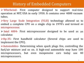
2. It defines what an embedded system is, discusses the hardware and software components, and classification of microprocessors.
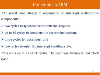
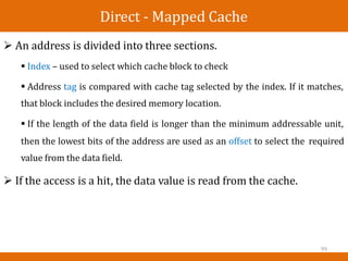
3. The document covers advantages of programmable CPUs, functionality of embedded systems, challenges in design, performance aspects, and formalisms for system design including UML.


![Pipelined execution of ARM Instructions
Extended execution is when an instruction is too complex to
complete the execution phase in a single cycle. Example: Multiple
load instruction (ldmia r0,[r2,r3])
135](https://image.slidesharecdn.com/unitiintroduction-230119035322-719bc38c/85/UNIT-I_Introduction-pptx-137-320.jpg)


![AMBA BUS in ARM
ARM has created a separate bus specification for single-chip
systems.
The AMBA bus [ARM99A] supports CPUs, memories, and
peripherals integrated in a system-on-silicon.
The AMBA specification includes two buses. The AMBA high-
performance bus (AHB) is optimized for high-speed transfers and is
directly connected to the CPU.
It supports several high-performance features: pipelining, burst
transfers, split transactions, and multiple bus masters.
189](https://image.slidesharecdn.com/unitiintroduction-230119035322-719bc38c/85/UNIT-I_Introduction-pptx-191-320.jpg)