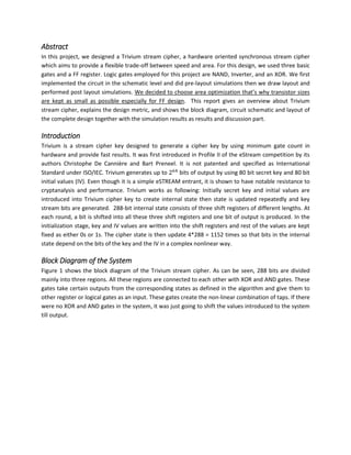
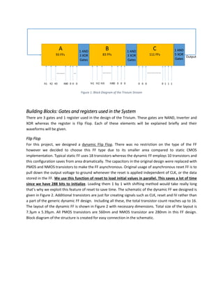
Download to read offline


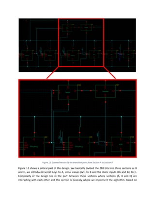


The document describes a project to design a Trivium stream cipher using Verilog. It includes: 1) A block diagram and description of the Trivium cipher design using flip flops, XOR, and AND gates. 2) Details of the flip flop, XOR gate, and AND gate designs used in the project. 3) The complete schematic showing how the components are connected to implement the Trivium cipher. 4) The layout of the full Trivium cipher design and post-layout simulation results showing correct functionality up to 700ns due to storage limitations.