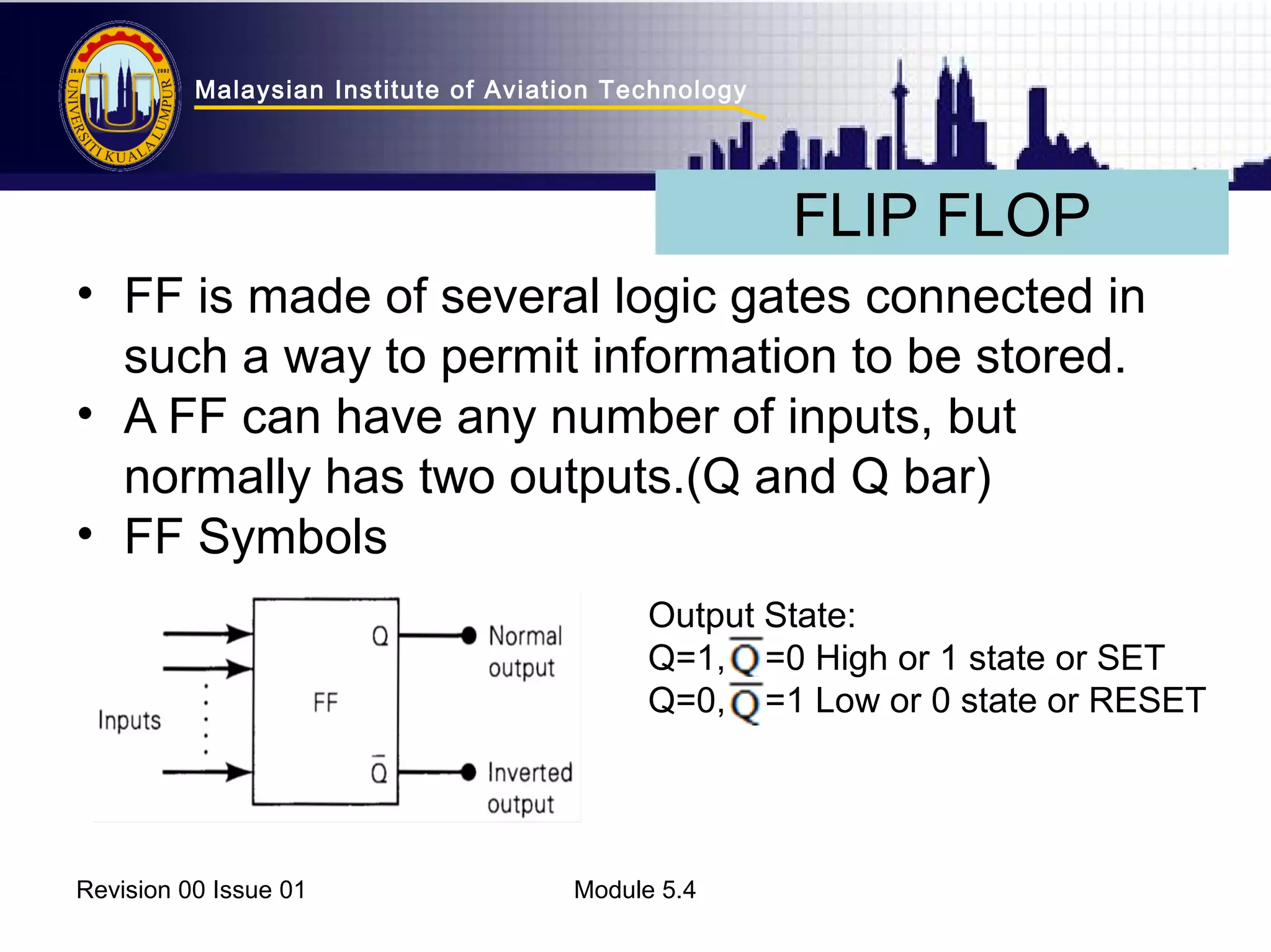
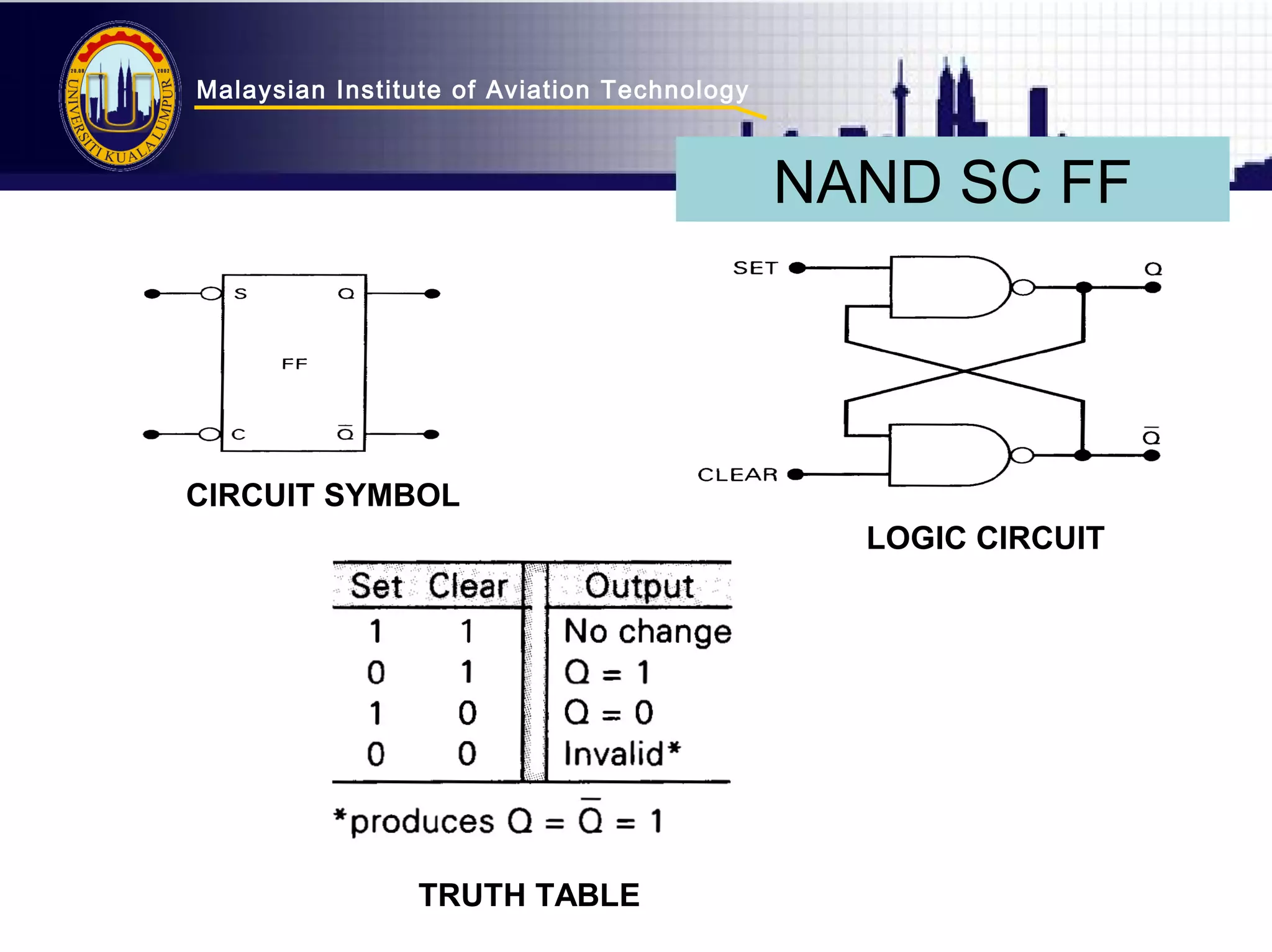
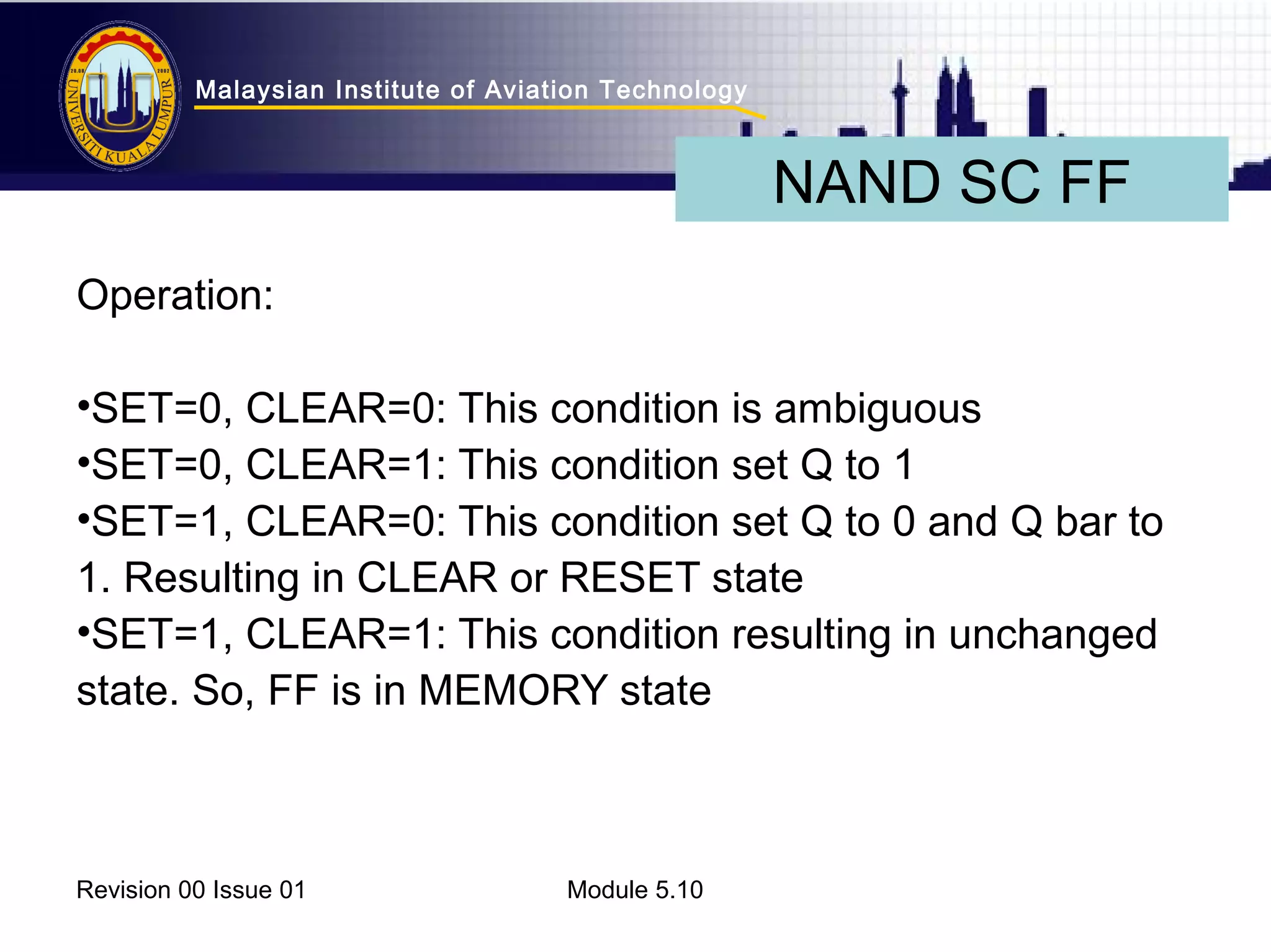
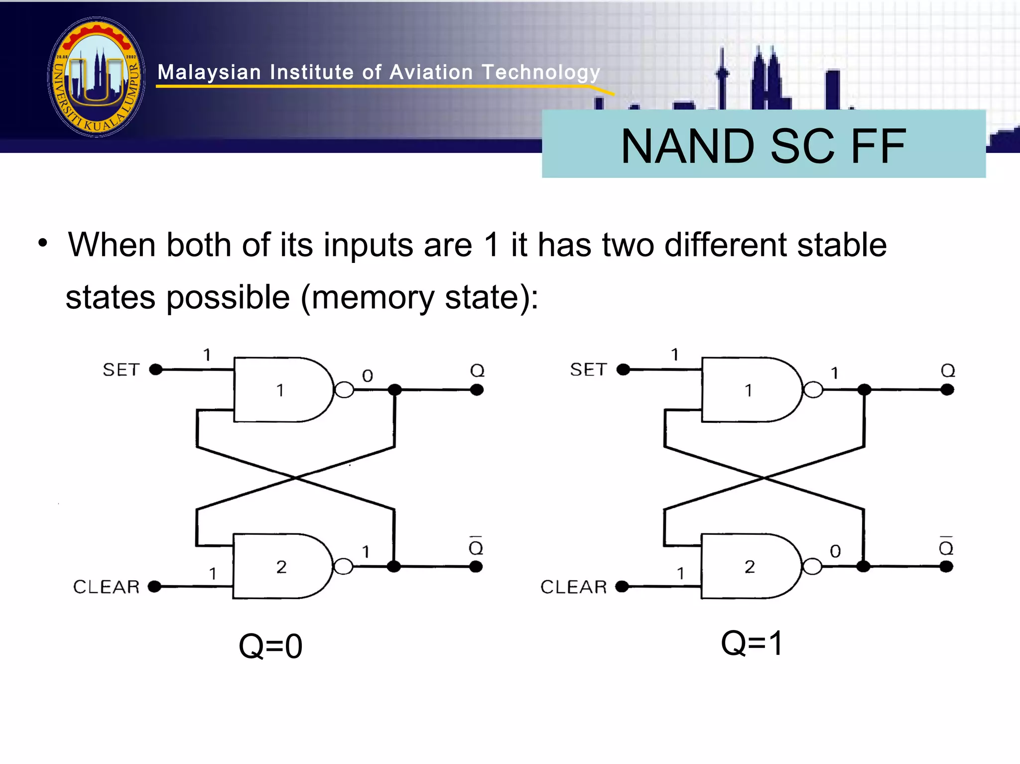
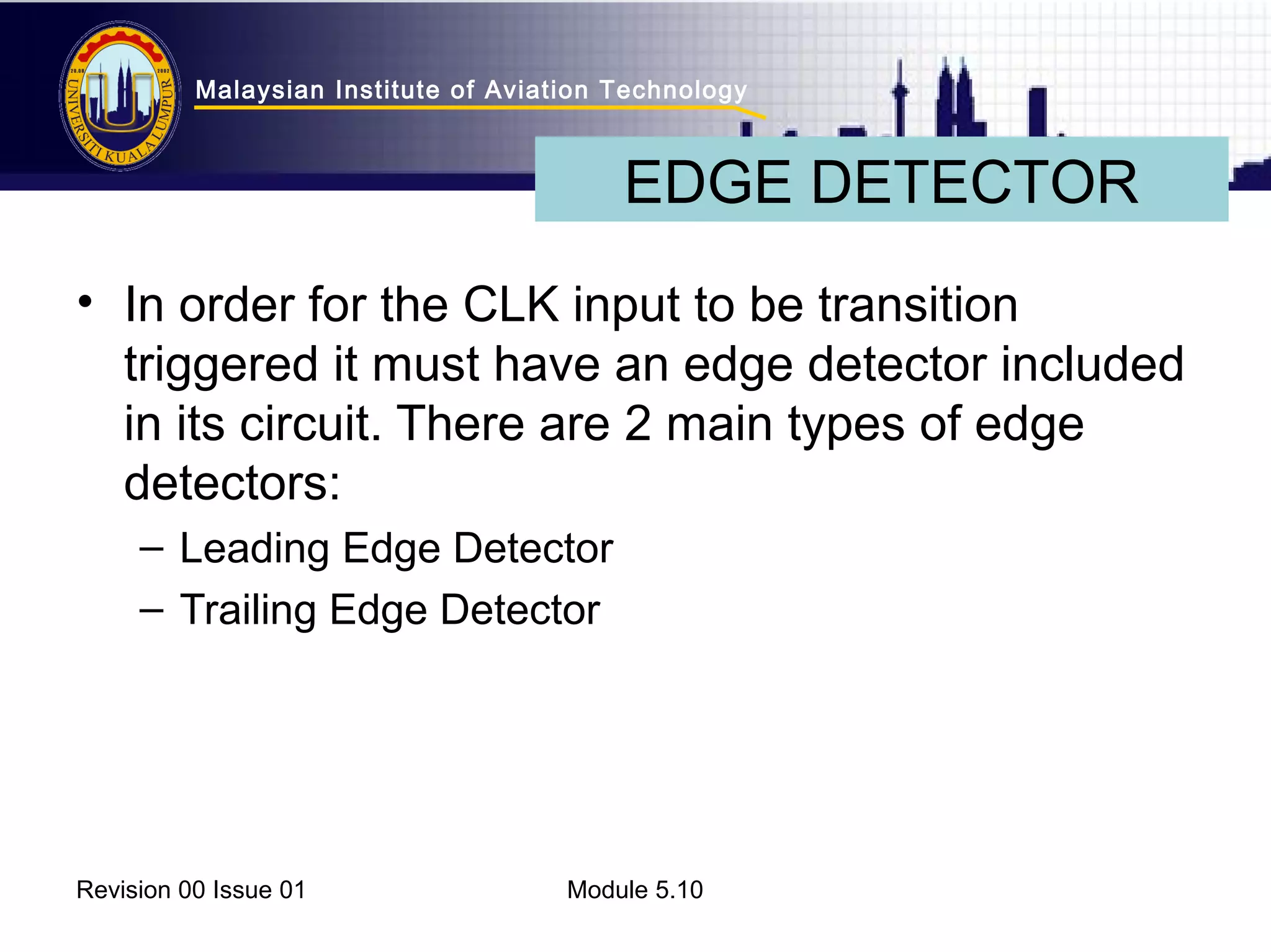
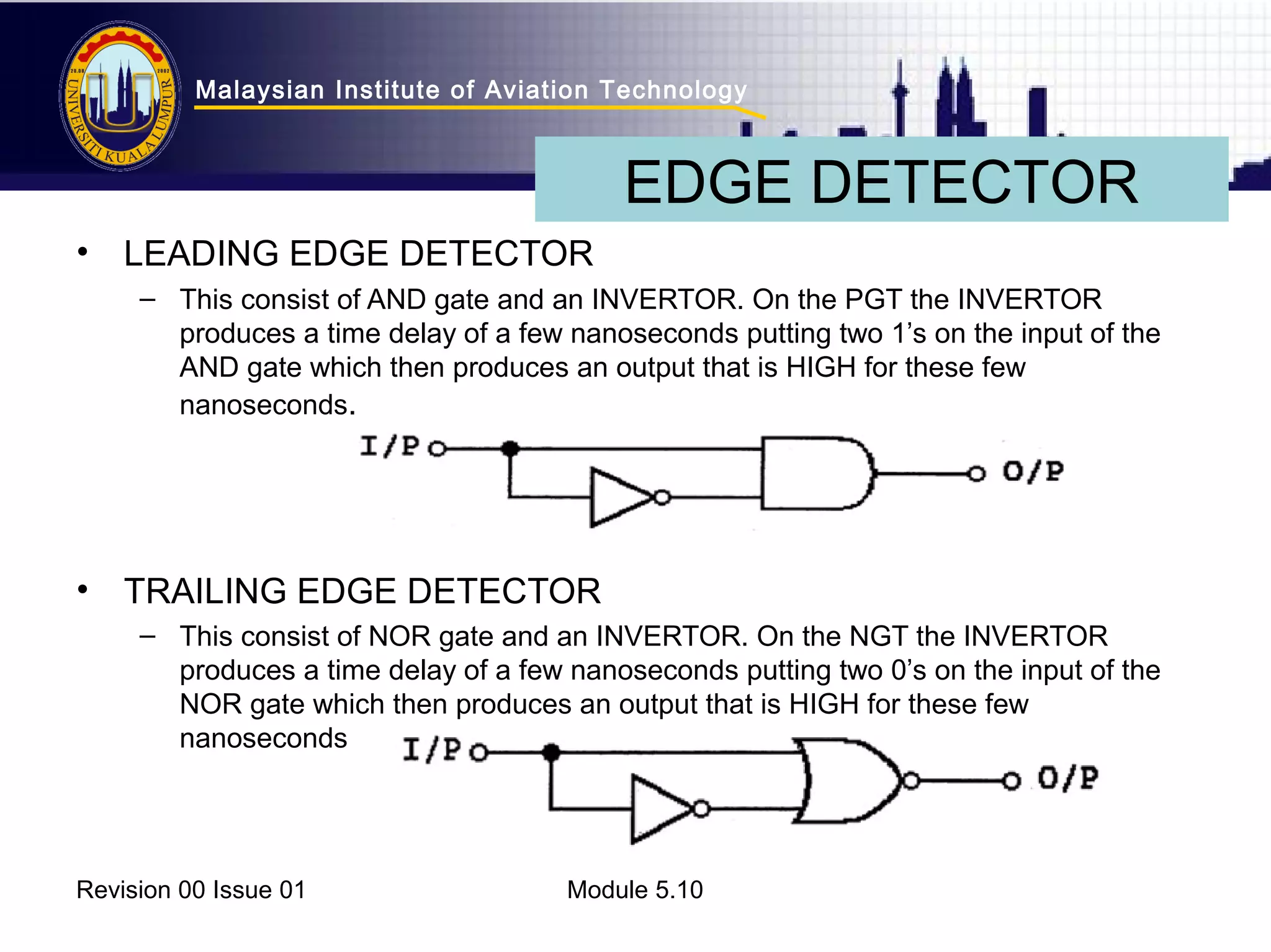
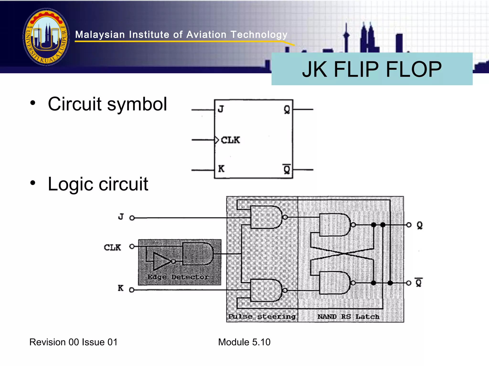
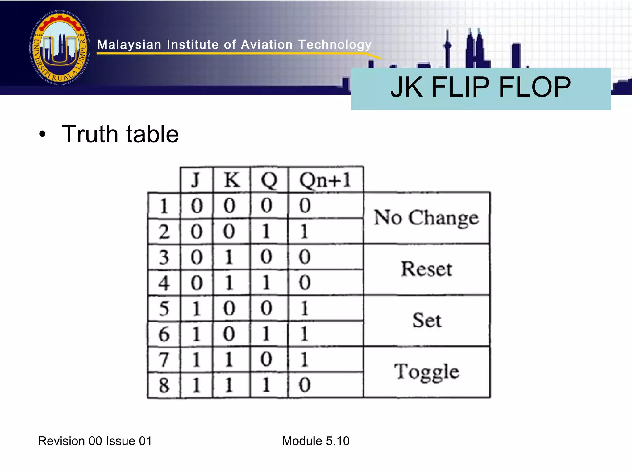
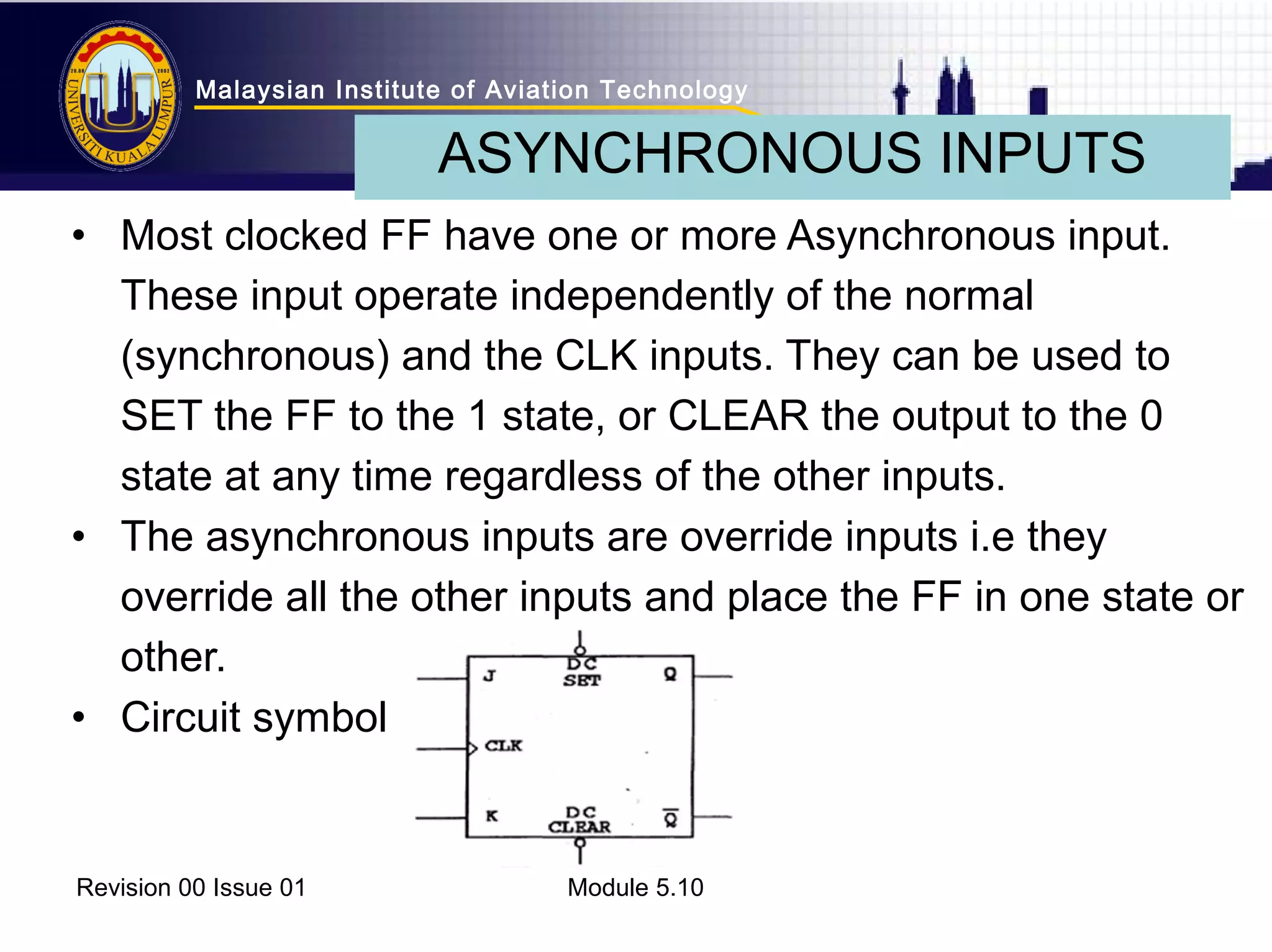
Malaysian Institute of Aviation Technology 
DIGITAL TECH (MECH) 
AKD 21102 
CHAPTER 3 
FLIP FLOP 
Revision 00 Issue 01 Module 5.4
Malaysian Institute of Aviation Technology 
LEARNING OUTCOME 
At the end of this topics, student should be able to: 
1.Understanding of flip flop terminologies 
2.Circuit symbol, truth table and operation of : 
– NAND and NOR SC (RS) Flip Flop 
– Clocked SC (RS) Flip flop 
– JK flip flop 
– JK flip flop with asynchronous input 
– D flip flop 
– D Latch 
– T flip flop 
1.Clock, PGT and NGT 
Revision 00 Issue 01 Module 5.4
Malaysian Institute of Aviation Technology 
WHAT IS FLIP FLOP? 
• Memory type circuits use flip-flops as their 
main components. 
• Flip-flop because on the application of a 
suitable pulse at the input(i/p), it causes the 
i/p to flip into one of it’s two stable states 
and stay in that state until a second input 
will flop it into its previous state. 
Revision 00 Issue 01 Module 5.10
Malaysian Institute of Aviation Technology 
• FF is made of several logic gates connected in 
such a way to permit information to be stored. 
• A FF can have any number of inputs, but 
normally has two outputs.(Q and Q bar) 
• FF Symbols 
Revision 00 Issue 01 Module 5.4 
FLIP FLOP 
Output State: 
Q=1, =0 High or 1 state or SET 
Q=0, =1 Low or 0 state or RESET
Malaysian Institute of Aviation Technology 
• State of FF is referring to Q. 
• If FF is HIGH, Q is HIGH or 1 (also called 
the SET state) 
• If FF is LOW, Q is LOW or 0 (CLEAR or 
RESET state) 
Revision 00 Issue 01 Module 5.10 
FLIP FLOP
Malaysian Institute of Aviation Technology 
LOGIC CIRCUIT 
CIRCUIT SYMBOL 
TRUTH TABLE 
NAND SC FF
Malaysian Institute of Aviation Technology 
Operation: 
•SET=0, CLEAR=0: This condition is ambiguous 
•SET=0, CLEAR=1: This condition set Q to 1 
•SET=1, CLEAR=0: This condition set Q to 0 and Q bar to 
1. Resulting in CLEAR or RESET state 
•SET=1, CLEAR=1: This condition resulting in unchanged 
state. So, FF is in MEMORY state 
Revision 00 Issue 01 Module 5.10 
NAND SC FF
Malaysian Institute of Aviation Technology 
NAND SC FF 
• When both of its inputs are 1 it has two different stable 
states possible (memory state): 
Q=0 Q=1
Malaysian Institute of Aviation Technology 
NAND SC FF TIMING DIAGRAM
Malaysian Institute of Aviation Technology 
NOR SC FF 
S C Q 
0 0 No change 
0 1 0 
1 0 1 
1 1 Invalid 
LOGIC CIRCUIT 
TRUTH TABLE 
CIRCUIT SYMBOL
Malaysian Institute of Aviation Technology 
Operation: 
•SET=0, CLEAR=0: This condition resulting in unchanged 
state. So, FF is in MEMORY state 
•SET=0, CLEAR=1: This condition set Q to 0 
•SET=1, CLEAR=0: This condition set Q to 1 and Q bar to 
0. Resulting in SET state 
•SET=1, CLEAR=1: This condition is ambiguous 
Revision 00 Issue 01 Module 5.10 
NOR SC FF
Malaysian Institute of Aviation Technology 
NOR SC FF 
• When both of its inputs are 0 it has two different 
stable states possible (memory) 
0 
1 
1 
0 
0 0 
0 
0 
0 
0 1 
1 
Q = 1 Q = 0
Malaysian Institute of Aviation Technology 
NOR SC FF TIMING DIAGRAM
Malaysian Institute of Aviation Technology 
• In sequential logic circuits where there may be a 
large number of flip-flops, it is important they all 
act at the same time so that no circuit operates 
out of sequence. 
• Achieved by a clock pulse which is derived from a 
pulse generator with a high frequency. 
• The circuit may be triggered when the clock 
pulse changes from 1 to 0 or from 0 to 1(edge 
triggered) or when the level is 1 or 0 
Revision 00 Issue 01 Module 5.10 
CLOCK
Malaysian Institute of Aviation Technology 
CLOCK SIGNAL 
• There are two types of sequential circuits: 
– Synchronous 
– Asynchronous 
• In synchronous logic there is a master oscillator 
(clock) that provides regular timing pulses. The 
output only change when the FF receives a clock 
pulse. 
• Asynchronous system, the outputs of the logic 
circuits can change state anytime the inputs 
change. 
Revision 00 Issue 01 Module 5.10
Malaysian Institute of Aviation Technology 
• Clocked FF has a clock input that is typically 
labelled CLK, CK, CP or C. 
• Most clocked FF’s are triggered by transition of 
the clock pulse and there are two types of 
transition. 
– Positive Going Transition (PGT) 
– Negative Going Transition (NGT) 
Revision 00 Issue 01 Module 5.10 
CLOCK SIGNAL
Malaysian Institute of Aviation Technology 
POSITIVE GOING TRANSITION (PGT) 
• The transition of a logic state (pulse) from 0 to 1 (sometime referred 
to as POSITIVE or LEADING EDGE TRIGGERING). 
• This indicated in circuit by a small triangle (>). 
• Circuit Symbol: 
• Timing diagram: 
Revision 00 Issue 01 Module 5.10
Malaysian Institute of Aviation Technology 
NEGATIVE GOING TRANSITION (NGT) 
• The transition of a logic state (pulse) from 1 to 0 (sometime referred 
to as NEGATIVE or TRAILING EDGE TRIGGERING). 
• This indicated in circuit by a circle and a small triangle (>). 
• Circuit Symbol: 
• Timing diagram: 
Revision 00 Issue 01 Module 5.10
Malaysian Institute of Aviation Technology 
CLOCK SC FLIP FLOP 
• A simple clocked SC FF can be constructed using 
two AND gates to direct the inputs into normal SC 
latch. 
• Logic circuit: 
Revision 00 Issue 01 Module 5.10
Malaysian Institute of Aviation Technology 
CLOCK SC FLIP FLOP 
S C Q Qn+1 Condition 
1 0 0 0 0 No change 
2 0 0 1 1 
3 0 1 0 0 Reset 
4 0 1 1 0 
5 1 0 0 1 Set 
6 1 0 1 1 
7 1 1 0 X Invalid 
8 1 1 1 X 
SC FF Truth Table
Malaysian Institute of Aviation Technology 
CLOCK SC FF 
Operation: 
•SET=1, CLEAR=0, CLK=0 to 1: No effect on FF’s output while CLK=0 because the output 
from the AND gate is 0. So, the NOR latch is in MEMORY state. When CLK=1, the AND 
gate are enable and FF flip to SET state 
•SET=1, CLEAR=0, CLK=1 to 0: No effect because when CLK=0, the AND gate gate is 0. 
So, the NOR latch is in MEMORY state. When CLK=1, the AND gate are disable and NOR 
latch is in MEMORY state 
•SET=0, CLEAR=1, CLK=0 to 1: No effect on FF’s output while CLK=0 because the output 
from the AND gate is 0. So, the NOR latch is in MEMORY state. When CLK=1, the AND 
gate are enable and FF flip to CLEAR or RESET state 
•SET=1, CLEAR=1: This condition is invalid and not normally used 
Revision 00 Issue 01 Module 5.10
Malaysian Institute of Aviation Technology 
CLOCK SC FF TIMING DIAGRAM
Malaysian Institute of Aviation Technology 
EDGE DETECTOR 
• In order for the CLK input to be transition 
triggered it must have an edge detector included 
in its circuit. There are 2 main types of edge 
detectors: 
– Leading Edge Detector 
– Trailing Edge Detector 
Revision 00 Issue 01 Module 5.10
Malaysian Institute of Aviation Technology 
• LEADING EDGE DETECTOR 
EDGE DETECTOR 
– This consist of AND gate and an INVERTOR. On the PGT the INVERTOR 
produces a time delay of a few nanoseconds putting two 1’s on the input of the 
AND gate which then produces an output that is HIGH for these few 
nanoseconds. 
• TRAILING EDGE DETECTOR 
– This consist of NOR gate and an INVERTOR. On the NGT the INVERTOR 
produces a time delay of a few nanoseconds putting two 0’s on the input of the 
NOR gate which then produces an output that is HIGH for these few 
nanoseconds 
Revision 00 Issue 01 Module 5.10
Malaysian Institute of Aviation Technology 
• By adding some additional gating to the SR FF the 
problem of the indeterminate state can be overcome. 
The FF without an indeterminate state is known as 
the JK Flip Flop. The set input is J and the reset input 
is K 
• A PGT triggered JK FF can be constructed in 3 parts: 
1. LEADING EDGE DETECTOR 
2. PULSE STEERING CIRCUIT 
• Consist of 2 three inputs NAND gate which the inputs are 
connected to 
– The CLK 
– J & K terminal respectively 
– Cross connected to the Q and Q bas. 
1. A NAND RS FF 
Revision 00 Issue 01 Module 5.10 
JK FLIP FLOP
Malaysian Institute of Aviation Technology 
• Circuit symbol 
• Logic circuit 
Revision 00 Issue 01 Module 5.10 
JK FLIP FLOP
Malaysian Institute of Aviation Technology 
• Truth table 
Revision 00 Issue 01 Module 5.10 
JK FLIP FLOP
Malaysian Institute of Aviation Technology 
CLOCK JK FLIP FLOP 
Operation 
•J=1, K=0, CLK=0 to 1: This condition does not effect the FF’s output while CLK=0 
because the output from the NAND Gate is 1, so the NAND latch is in the memory 
state. When the CLK goes to 1 the NAND Gates are enabled so the FF will then flip 
to its SET state. (Q=1) 
•J=1, K=0, CLK=1 to 0: This condition has no effect on the FF’s output because 
when CLK=0 or 1 the NAND Gates are disable and the NAND latch is in memory 
state. 
•J=0, K=1, CLK=0 to 1: This condition does not effect the FF’s output while CLK=0 
because the output from the NAND Gates are disable, so the NAND latch is in the 
memory state. When the CLK goes to 1 the AND Gates are enabled so the FF will 
then flip to its CLEAR or RESET state. (Q=0) 
•J=0, K=0: With this input the output from the NAND gates will be 1 irrespective of 
the CLK so the FF in the memory state. 
•J=1, K=1: This condition does not effect the FF’s output while CLK=0 because the 
NAND gates are disable and the NAND latch is in the memory state. During the 
PGT of the CLK pulse the NAND gates are enable and the FF’s output will go to its 
opposite state. This the TOGGLE mode of operation. 
Revision 00 Issue 01 Module 5.10
Malaysian Institute of Aviation Technology 
J 
K 
CLK 
Q 
CLOCK JK FLIP FLOP TIMING DIAGRAM
Malaysian Institute of Aviation Technology 
CLOCK D FLIP FLOP 
• Can be constructed using a J-K FF, adding an 
INVERTOR to the K input and connecting both 
input together. 
• Circuit symbol 
• Logic circuit 
Revision 00 Issue 01 Module 5.10
Malaysian Institute of Aviation Technology 
CLOCK D FLIP FLOP 
• What ever data is placed at the D input is then 
latched(delay) to the Q output after CLK. 
• Truth table 
Revision 00 Issue 01 Module 5.10
Malaysian Institute of Aviation Technology 
D LATCH FLIP FLOP 
• Can be constructed using an INVERTOR and two 
NAND gates to direct the input to a normal NAND 
latch. 
• Circuit symbol 
• Logic circuit 
Revision 00 Issue 01 Module 5.10
Malaysian Institute of Aviation Technology 
D LATCH FF OPERATION 
• With a D latch the common input to the steering 
NAND gates is called ENABLE (EN) input because 
its effect on the output is not restricted to its 
transition. 
• D latch has two operating conditions 
– When the EN input is HIGH, Q will become same level as 
D and will follow any changes in the D input. In this mode 
the D latch is said to be TRANSPARENT 
– When the EN input is LOW, the D input in inhibited so the 
output will stay at whatever level they has when EN when 
low. In this mode the output is said to be LATCHED. 
Revision 00 Issue 01 Module 5.10
Malaysian Institute of Aviation Technology 
• Toggling is an action that changes a device between its 
two output state on each consecutive operation of its 
control line. 
• The operation of the FF in toggle mode relies on placing 
the inverse of the output to the input after each clock 
edge. The input to the toggle is the clock signal and the 
output is taken from either the Q or Q bar terminal. 
Revision 00 Issue 01 Module 5.10 
T FLIP FLOP
Malaysian Institute of Aviation Technology 
Factor Affecting FF Reliability 
• The output of a clocked FF is dependent on both the 
Synchronous and Clock inputs there are some other 
factors which must be taken into account if the FF is to 
operate with reliability. 
• Set Up time 
• Hold time 
• Propagation Delay 
• Maximum Clocking Frequency 
Revision 00 Issue 01 Module 5.10
Malaysian Institute of Aviation Technology 
• Set-up Time (ts): This is the time interval immediately 
preceding the active transition of the clock pulse during 
the synchronous input has to be kept at the proper level to 
ensure triggering of the FF. 
Revision 00 Issue 01 Module 5.10 
SET UP TIME
Malaysian Institute of Aviation Technology 
• Hold Time (th): This is the time interval immediately 
following the active transition of the clock pulse during the 
synchronous input has to be kept at the proper level to 
ensure triggering of the FF. 
Revision 00 Issue 01 Module 5.10 
HOLD TIME
Malaysian Institute of Aviation Technology 
PROPAGATION DELAY 
• Propagation delay (tPLH): This is the delay in a FF from 
when the input signal is applied to and then output makes 
its changes. 
• These delays are measure between the 50% point on the 
waveform 
Delay going from 0 to 1 Delay going from 1 to 0 
Revision 00 Issue 01 Module 5.10
Malaysian Institute of Aviation Technology 
MAXIMUM CLOCK FREQUENCY 
• The highest frequency that may be applied to the 
clock input of a FF and still have trigger reliability. 
Revision 00 Issue 01 Module 5.10
Malaysian Institute of Aviation Technology 
ASYNCHRONOUS INPUTS 
• Most clocked FF have one or more Asynchronous input. 
These input operate independently of the normal 
(synchronous) and the CLK inputs. They can be used to 
SET the FF to the 1 state, or CLEAR the output to the 0 
state at any time regardless of the other inputs. 
• The asynchronous inputs are override inputs i.e they 
override all the other inputs and place the FF in one state or 
other. 
• Circuit symbol 
Revision 00 Issue 01 Module 5.10
Malaysian Institute of Aviation Technology 
ASYNCHRONOUS INPUTS 
• The asynchronous inputs are level triggered so they 
hold the output in the SET or CLEAR state while ever 
there is a LOW on the DC SET or DC CLEAR inputs. 
• Thus, the asynchronous inputs can be used to hold the 
FF in a particular state for any desired interval. 
• However, the asynchronous inputs are most often used 
to SET or CLEAR the FF to the desired state by the 
application of a momentary pulse. 
Revision 00 Issue 01 Module 5.10

Topic 3 Digital Technique Flip flop

  • 1.
    Malaysian Institute ofAviation Technology DIGITAL TECH (MECH) AKD 21102 CHAPTER 3 FLIP FLOP Revision 00 Issue 01 Module 5.4
  • 2.
    Malaysian Institute ofAviation Technology LEARNING OUTCOME At the end of this topics, student should be able to: 1.Understanding of flip flop terminologies 2.Circuit symbol, truth table and operation of : – NAND and NOR SC (RS) Flip Flop – Clocked SC (RS) Flip flop – JK flip flop – JK flip flop with asynchronous input – D flip flop – D Latch – T flip flop 1.Clock, PGT and NGT Revision 00 Issue 01 Module 5.4
  • 3.
    Malaysian Institute ofAviation Technology Malaysian Institute of Aviation Technology WHAT IS FLIP FLOP? • Memory type circuits use flip-flops as their main components. • Flip-flop because on the application of a suitable pulse at the input(i/p), it causes the i/p to flip into one of it’s two stable states and stay in that state until a second input will flop it into its previous state. Revision 00 Issue 01 Module 5.10
  • 4.
    Malaysian Institute ofAviation Technology • FF is made of several logic gates connected in such a way to permit information to be stored. • A FF can have any number of inputs, but normally has two outputs.(Q and Q bar) • FF Symbols Revision 00 Issue 01 Module 5.4 FLIP FLOP Output State: Q=1, =0 High or 1 state or SET Q=0, =1 Low or 0 state or RESET
  • 5.
    Malaysian Institute ofAviation Technology • State of FF is referring to Q. • If FF is HIGH, Q is HIGH or 1 (also called the SET state) • If FF is LOW, Q is LOW or 0 (CLEAR or RESET state) Revision 00 Issue 01 Module 5.10 FLIP FLOP
  • 6.
    Malaysian Institute ofAviation Technology LOGIC CIRCUIT CIRCUIT SYMBOL TRUTH TABLE NAND SC FF
  • 7.
    Malaysian Institute ofAviation Technology Operation: •SET=0, CLEAR=0: This condition is ambiguous •SET=0, CLEAR=1: This condition set Q to 1 •SET=1, CLEAR=0: This condition set Q to 0 and Q bar to 1. Resulting in CLEAR or RESET state •SET=1, CLEAR=1: This condition resulting in unchanged state. So, FF is in MEMORY state Revision 00 Issue 01 Module 5.10 NAND SC FF
  • 8.
    Malaysian Institute ofAviation Technology NAND SC FF • When both of its inputs are 1 it has two different stable states possible (memory state): Q=0 Q=1
  • 9.
    Malaysian Institute ofAviation Technology NAND SC FF TIMING DIAGRAM
  • 10.
    Malaysian Institute ofAviation Technology NOR SC FF S C Q 0 0 No change 0 1 0 1 0 1 1 1 Invalid LOGIC CIRCUIT TRUTH TABLE CIRCUIT SYMBOL
  • 11.
    Malaysian Institute ofAviation Technology Operation: •SET=0, CLEAR=0: This condition resulting in unchanged state. So, FF is in MEMORY state •SET=0, CLEAR=1: This condition set Q to 0 •SET=1, CLEAR=0: This condition set Q to 1 and Q bar to 0. Resulting in SET state •SET=1, CLEAR=1: This condition is ambiguous Revision 00 Issue 01 Module 5.10 NOR SC FF
  • 12.
    Malaysian Institute ofAviation Technology NOR SC FF • When both of its inputs are 0 it has two different stable states possible (memory) 0 1 1 0 0 0 0 0 0 0 1 1 Q = 1 Q = 0
  • 13.
    Malaysian Institute ofAviation Technology NOR SC FF TIMING DIAGRAM
  • 14.
    Malaysian Institute ofAviation Technology • In sequential logic circuits where there may be a large number of flip-flops, it is important they all act at the same time so that no circuit operates out of sequence. • Achieved by a clock pulse which is derived from a pulse generator with a high frequency. • The circuit may be triggered when the clock pulse changes from 1 to 0 or from 0 to 1(edge triggered) or when the level is 1 or 0 Revision 00 Issue 01 Module 5.10 CLOCK
  • 15.
    Malaysian Institute ofAviation Technology CLOCK SIGNAL • There are two types of sequential circuits: – Synchronous – Asynchronous • In synchronous logic there is a master oscillator (clock) that provides regular timing pulses. The output only change when the FF receives a clock pulse. • Asynchronous system, the outputs of the logic circuits can change state anytime the inputs change. Revision 00 Issue 01 Module 5.10
  • 16.
    Malaysian Institute ofAviation Technology • Clocked FF has a clock input that is typically labelled CLK, CK, CP or C. • Most clocked FF’s are triggered by transition of the clock pulse and there are two types of transition. – Positive Going Transition (PGT) – Negative Going Transition (NGT) Revision 00 Issue 01 Module 5.10 CLOCK SIGNAL
  • 17.
    Malaysian Institute ofAviation Technology POSITIVE GOING TRANSITION (PGT) • The transition of a logic state (pulse) from 0 to 1 (sometime referred to as POSITIVE or LEADING EDGE TRIGGERING). • This indicated in circuit by a small triangle (>). • Circuit Symbol: • Timing diagram: Revision 00 Issue 01 Module 5.10
  • 18.
    Malaysian Institute ofAviation Technology NEGATIVE GOING TRANSITION (NGT) • The transition of a logic state (pulse) from 1 to 0 (sometime referred to as NEGATIVE or TRAILING EDGE TRIGGERING). • This indicated in circuit by a circle and a small triangle (>). • Circuit Symbol: • Timing diagram: Revision 00 Issue 01 Module 5.10
  • 19.
    Malaysian Institute ofAviation Technology CLOCK SC FLIP FLOP • A simple clocked SC FF can be constructed using two AND gates to direct the inputs into normal SC latch. • Logic circuit: Revision 00 Issue 01 Module 5.10
  • 20.
    Malaysian Institute ofAviation Technology CLOCK SC FLIP FLOP S C Q Qn+1 Condition 1 0 0 0 0 No change 2 0 0 1 1 3 0 1 0 0 Reset 4 0 1 1 0 5 1 0 0 1 Set 6 1 0 1 1 7 1 1 0 X Invalid 8 1 1 1 X SC FF Truth Table
  • 21.
    Malaysian Institute ofAviation Technology CLOCK SC FF Operation: •SET=1, CLEAR=0, CLK=0 to 1: No effect on FF’s output while CLK=0 because the output from the AND gate is 0. So, the NOR latch is in MEMORY state. When CLK=1, the AND gate are enable and FF flip to SET state •SET=1, CLEAR=0, CLK=1 to 0: No effect because when CLK=0, the AND gate gate is 0. So, the NOR latch is in MEMORY state. When CLK=1, the AND gate are disable and NOR latch is in MEMORY state •SET=0, CLEAR=1, CLK=0 to 1: No effect on FF’s output while CLK=0 because the output from the AND gate is 0. So, the NOR latch is in MEMORY state. When CLK=1, the AND gate are enable and FF flip to CLEAR or RESET state •SET=1, CLEAR=1: This condition is invalid and not normally used Revision 00 Issue 01 Module 5.10
  • 22.
    Malaysian Institute ofAviation Technology CLOCK SC FF TIMING DIAGRAM
  • 23.
    Malaysian Institute ofAviation Technology EDGE DETECTOR • In order for the CLK input to be transition triggered it must have an edge detector included in its circuit. There are 2 main types of edge detectors: – Leading Edge Detector – Trailing Edge Detector Revision 00 Issue 01 Module 5.10
  • 24.
    Malaysian Institute ofAviation Technology • LEADING EDGE DETECTOR EDGE DETECTOR – This consist of AND gate and an INVERTOR. On the PGT the INVERTOR produces a time delay of a few nanoseconds putting two 1’s on the input of the AND gate which then produces an output that is HIGH for these few nanoseconds. • TRAILING EDGE DETECTOR – This consist of NOR gate and an INVERTOR. On the NGT the INVERTOR produces a time delay of a few nanoseconds putting two 0’s on the input of the NOR gate which then produces an output that is HIGH for these few nanoseconds Revision 00 Issue 01 Module 5.10
  • 25.
    Malaysian Institute ofAviation Technology • By adding some additional gating to the SR FF the problem of the indeterminate state can be overcome. The FF without an indeterminate state is known as the JK Flip Flop. The set input is J and the reset input is K • A PGT triggered JK FF can be constructed in 3 parts: 1. LEADING EDGE DETECTOR 2. PULSE STEERING CIRCUIT • Consist of 2 three inputs NAND gate which the inputs are connected to – The CLK – J & K terminal respectively – Cross connected to the Q and Q bas. 1. A NAND RS FF Revision 00 Issue 01 Module 5.10 JK FLIP FLOP
  • 26.
    Malaysian Institute ofAviation Technology • Circuit symbol • Logic circuit Revision 00 Issue 01 Module 5.10 JK FLIP FLOP
  • 27.
    Malaysian Institute ofAviation Technology • Truth table Revision 00 Issue 01 Module 5.10 JK FLIP FLOP
  • 28.
    Malaysian Institute ofAviation Technology CLOCK JK FLIP FLOP Operation •J=1, K=0, CLK=0 to 1: This condition does not effect the FF’s output while CLK=0 because the output from the NAND Gate is 1, so the NAND latch is in the memory state. When the CLK goes to 1 the NAND Gates are enabled so the FF will then flip to its SET state. (Q=1) •J=1, K=0, CLK=1 to 0: This condition has no effect on the FF’s output because when CLK=0 or 1 the NAND Gates are disable and the NAND latch is in memory state. •J=0, K=1, CLK=0 to 1: This condition does not effect the FF’s output while CLK=0 because the output from the NAND Gates are disable, so the NAND latch is in the memory state. When the CLK goes to 1 the AND Gates are enabled so the FF will then flip to its CLEAR or RESET state. (Q=0) •J=0, K=0: With this input the output from the NAND gates will be 1 irrespective of the CLK so the FF in the memory state. •J=1, K=1: This condition does not effect the FF’s output while CLK=0 because the NAND gates are disable and the NAND latch is in the memory state. During the PGT of the CLK pulse the NAND gates are enable and the FF’s output will go to its opposite state. This the TOGGLE mode of operation. Revision 00 Issue 01 Module 5.10
  • 29.
    Malaysian Institute ofAviation Technology J K CLK Q CLOCK JK FLIP FLOP TIMING DIAGRAM
  • 30.
    Malaysian Institute ofAviation Technology CLOCK D FLIP FLOP • Can be constructed using a J-K FF, adding an INVERTOR to the K input and connecting both input together. • Circuit symbol • Logic circuit Revision 00 Issue 01 Module 5.10
  • 31.
    Malaysian Institute ofAviation Technology CLOCK D FLIP FLOP • What ever data is placed at the D input is then latched(delay) to the Q output after CLK. • Truth table Revision 00 Issue 01 Module 5.10
  • 32.
    Malaysian Institute ofAviation Technology D LATCH FLIP FLOP • Can be constructed using an INVERTOR and two NAND gates to direct the input to a normal NAND latch. • Circuit symbol • Logic circuit Revision 00 Issue 01 Module 5.10
  • 33.
    Malaysian Institute ofAviation Technology D LATCH FF OPERATION • With a D latch the common input to the steering NAND gates is called ENABLE (EN) input because its effect on the output is not restricted to its transition. • D latch has two operating conditions – When the EN input is HIGH, Q will become same level as D and will follow any changes in the D input. In this mode the D latch is said to be TRANSPARENT – When the EN input is LOW, the D input in inhibited so the output will stay at whatever level they has when EN when low. In this mode the output is said to be LATCHED. Revision 00 Issue 01 Module 5.10
  • 34.
    Malaysian Institute ofAviation Technology • Toggling is an action that changes a device between its two output state on each consecutive operation of its control line. • The operation of the FF in toggle mode relies on placing the inverse of the output to the input after each clock edge. The input to the toggle is the clock signal and the output is taken from either the Q or Q bar terminal. Revision 00 Issue 01 Module 5.10 T FLIP FLOP
  • 35.
    Malaysian Institute ofAviation Technology Factor Affecting FF Reliability • The output of a clocked FF is dependent on both the Synchronous and Clock inputs there are some other factors which must be taken into account if the FF is to operate with reliability. • Set Up time • Hold time • Propagation Delay • Maximum Clocking Frequency Revision 00 Issue 01 Module 5.10
  • 36.
    Malaysian Institute ofAviation Technology • Set-up Time (ts): This is the time interval immediately preceding the active transition of the clock pulse during the synchronous input has to be kept at the proper level to ensure triggering of the FF. Revision 00 Issue 01 Module 5.10 SET UP TIME
  • 37.
    Malaysian Institute ofAviation Technology • Hold Time (th): This is the time interval immediately following the active transition of the clock pulse during the synchronous input has to be kept at the proper level to ensure triggering of the FF. Revision 00 Issue 01 Module 5.10 HOLD TIME
  • 38.
    Malaysian Institute ofAviation Technology PROPAGATION DELAY • Propagation delay (tPLH): This is the delay in a FF from when the input signal is applied to and then output makes its changes. • These delays are measure between the 50% point on the waveform Delay going from 0 to 1 Delay going from 1 to 0 Revision 00 Issue 01 Module 5.10
  • 39.
    Malaysian Institute ofAviation Technology MAXIMUM CLOCK FREQUENCY • The highest frequency that may be applied to the clock input of a FF and still have trigger reliability. Revision 00 Issue 01 Module 5.10
  • 40.
    Malaysian Institute ofAviation Technology ASYNCHRONOUS INPUTS • Most clocked FF have one or more Asynchronous input. These input operate independently of the normal (synchronous) and the CLK inputs. They can be used to SET the FF to the 1 state, or CLEAR the output to the 0 state at any time regardless of the other inputs. • The asynchronous inputs are override inputs i.e they override all the other inputs and place the FF in one state or other. • Circuit symbol Revision 00 Issue 01 Module 5.10
  • 41.
    Malaysian Institute ofAviation Technology ASYNCHRONOUS INPUTS • The asynchronous inputs are level triggered so they hold the output in the SET or CLEAR state while ever there is a LOW on the DC SET or DC CLEAR inputs. • Thus, the asynchronous inputs can be used to hold the FF in a particular state for any desired interval. • However, the asynchronous inputs are most often used to SET or CLEAR the FF to the desired state by the application of a momentary pulse. Revision 00 Issue 01 Module 5.10