This document describes the fabrication and testing of surface acoustic wave (SAW) devices. Five SAW devices were fabricated in a cleanroom using thin film deposition, photolithography, and wet etching processes. The devices were then tested as filters by measuring their bandwidth and operating frequencies using a network analyzer. Additionally, the potential for SAW devices to be used as biosensors was demonstrated by measuring frequency shifts when biotin solution was deposited on a quartz crystal microbalance, showing detection of added mass.
![1
Cleanroom Fabrication and Applications of Surface Acoustic
Wave Devices
Nitasha Goyal Madelyn Hutton Kevin Mao
nitashagoyal27@gmail.com maddyrhutton@yahoo.com kevinmao7@gmail.com
Walter Roper Soumya Sudhakar
wroper9910@gmail.com soumya96@gmail.com
Abstract
Beyond traditional uses as filters in radios and
cell phones, surface acoustic wave (SAW)
devices have applications in the medical field
as biosensors. Five SAW devices were
fabricated in the Rutgers MERL cleanroom
through the processes of thin film deposition,
photolithography, and wet etching.
Measurements of the bandwidths using 3
decibel (dB) width calculations and
measurements of operating frequencies of the
SAW devices showed functionality as filters.
Measurements of the mass of biotin
demonstrate the potential use of SAW devices
as microbalances and biosensors.
1 Introduction
Nanotechnology and microfabrication
have gained importance in today’s world since
the fields enable machines to be more energy
and cost efficient. One type of device in this
field is the surface acoustic wave (SAW)
device. Most commonly, SAW devices act as
frequency filters in instruments such as cell
phones and radios, selecting only a certain
bandwidth of frequencies. Today, research is
being conducted using SAW devices as
biosensors. Biosensors can be microbalances
that measure the mass of objects on a
microscale such as a strand of DNA. In
addition to aiding in genetic research such as
DNA hybridization, SAW devices can help
diabetic patients in blood glucose testing by
substantially reducing the amount of blood
collected. Some recent research is focused on
SAW devices’ ability to improve the efficiency
of solar panels[1]. In this work, SAW devices
were demonstrated successfully as filters and
used in the biosensing application as
microbalances.
2 Background
The microfabrication procedure has
been successfully improved in both research
and industry in the past decades. Our SAW
devices were fabricated in the cleanroom at
Rutgers’ Microelectronics Research
Laboratory (MERL).
2.1 The Cleanroom
A cleanroom is a lab in which certain
environmental pollutants are highly
controlled. This type of lab is commonly used
in fields that are sensitive to ecological
contamination such as semiconductor
manufacturing, biotechnology, and
microfabrication processes[2]. Despite its
name, cleanrooms are not sterile; rather, they
have a controlled level of airborne
contamination. Airflow rates and direction,
pressurization, temperature, humidity and
filtration are regulated to keep pollutants at a
minimum[3].
A cleanroom is necessary for the
fabrication process in order to preserve the
integrity of the devices made. Dust particles
in the air can interfere with the fabrication of
SAW devices during the fabrication process.
Since the SAW devices are on the microscale,
these dust particles are large enough to cause
the devices to be defective[4]. In addition to](https://image.slidesharecdn.com/2142ebb7-c0f8-4580-ae2c-0ae145f7d634-160521180355/85/Surface-Acoustic-Wave-Devices-1-320.jpg)
![1
Cleanroom Fabrication and Applications of Surface Acoustic
Wave Devices
Nitasha Goyal Madelyn Hutton Kevin Mao
nitashagoyal27@gmail.com maddyrhutton@yahoo.com kevinmao7@gmail.com
Walter Roper Soumya Sudhakar
wroper9910@gmail.com soumya96@gmail.com
Abstract
Beyond traditional uses as filters in radios and
cell phones, surface acoustic wave (SAW)
devices have applications in the medical field
as biosensors. Five SAW devices were
fabricated in the Rutgers MERL cleanroom
through the processes of thin film deposition,
photolithography, and wet etching.
Measurements of the bandwidths using 3
decibel (dB) width calculations and
measurements of operating frequencies of the
SAW devices showed functionality as filters.
Measurements of the mass of biotin
demonstrate the potential use of SAW devices
as microbalances and biosensors.
1 Introduction
Nanotechnology and microfabrication
have gained importance in today’s world since
the fields enable machines to be more energy
and cost efficient. One type of device in this
field is the surface acoustic wave (SAW)
device. Most commonly, SAW devices act as
frequency filters in instruments such as cell
phones and radios, selecting only a certain
bandwidth of frequencies. Today, research is
being conducted using SAW devices as
biosensors. Biosensors can be microbalances
that measure the mass of objects on a
microscale such as a strand of DNA. In
addition to aiding in genetic research such as
DNA hybridization, SAW devices can help
diabetic patients in blood glucose testing by
substantially reducing the amount of blood
collected. Some recent research is focused on
SAW devices’ ability to improve the efficiency
of solar panels[1]. In this work, SAW devices
were demonstrated successfully as filters and
used in the biosensing application as
microbalances.
2 Background
The microfabrication procedure has
been successfully improved in both research
and industry in the past decades. Our SAW
devices were fabricated in the cleanroom at
Rutgers’ Microelectronics Research
Laboratory (MERL).
2.1 The Cleanroom
A cleanroom is a lab in which certain
environmental pollutants are highly
controlled. This type of lab is commonly used
in fields that are sensitive to ecological
contamination such as semiconductor
manufacturing, biotechnology, and
microfabrication processes[2]. Despite its
name, cleanrooms are not sterile; rather, they
have a controlled level of airborne
contamination. Airflow rates and direction,
pressurization, temperature, humidity and
filtration are regulated to keep pollutants at a
minimum[3].
A cleanroom is necessary for the
fabrication process in order to preserve the
integrity of the devices made. Dust particles
in the air can interfere with the fabrication of
SAW devices during the fabrication process.
Since the SAW devices are on the microscale,
these dust particles are large enough to cause
the devices to be defective[4]. In addition to](https://image.slidesharecdn.com/2142ebb7-c0f8-4580-ae2c-0ae145f7d634-160521180355/75/Surface-Acoustic-Wave-Devices-1-2048.jpg)
![2
dust, other particulates in air, such as smoke,
bacteria, and cells, can also cause similar
problems in the devices. For these reasons,
microfabrication processes are carried out in
cleanrooms where the number of particulates
in the air can be controlled, decreasing the
probability of defective devices.
2.2 Surface Acoustic Wave Devices
SAW filters utilize interdigital
transducers (IDTs) and piezoelectricity to
produce surface acoustic waves.
IDTs consist of finger-like patterns
made of conductive material, such as
aluminum, as seen in Figure 2.1, and are used
to generate and receive the surface acoustic
waves. The number of fingers, the spacing
between the fingers, and the spacing between
the IDTs determines which frequencies are
able to travel through the circuit effectively.
Figure 2.1 Blue represents the IDTs of the SAW
device while yellow represents the quartz delay line.
Courtesy of Zheng Zhang, Rutgers University.
The SAW device utilizes the
piezoelectric effect by converting electrical
energy (AC voltage) to mechanical energy at
one end of the device and converting back to
electrical energy at the other end. The
piezoelectric effect refers to the electric
charge in response to pressure due to dipole
formation in the crystal lattice. The effect is
reversible; the inverse piezoelectric effect
results in the generation of mechanical strain
from an applied electric field. Voltage across
the input IDT generates a current which
energizes the quartz underneath the IDT
fingers. Quartz is a piezoelectric material. The
electrical energy is converted into mechanical
energy waves due to the contraction of the
quartz. The waves travel across the quartz to
the output IDT. The output IDT then
converts the mechanical waves back to
electrical energy, resulting in a voltage.
SAW-based processors are
lightweight and versatile and have low energy
consumption; therefore, they are
advantageous to use in portable wireless
communication devices[4].
2.3 Usage of SAW Devices as
Filters
One common use of SAW devices is
as filters found in appliances such as radios and
cell phones.
SAW devices filter frequencies
through the basic principles of wave
interference. When waves are in phase across
the device, they cause constructive
interference and are allowed through the
device. When waves are out of phase across
the device, they cause destructive interference
and are filtered[5]. The phase coherence
depends on the frequency of the waves (or the
wavelength), the distance between the IDTs
and the IDT periodicity.
2.4 Quartz Crystal Microbalance
A new area of research involves using
acoustic wave devices as biosensors to
determine the mass of objects. In this work,
this application was demonstrated using the
quartz crystal microbalance (QCM). QCM is
also a piezoelectric device, but uses acoustic
waves propagating longitudinally rather than
tranversely. The biosensors in Figure 2.2
work since QCM devices can detect changes
in frequency. Using Equation 1, it is possible
to determine the change in mass.
Equation 1
= 3.336x10³
m/s (acoustic velocity of quartz)
= 2.648x10³
(density of quartz)
= 0.2047 cm3
(area of quartz)
= change in frequency
= fundamental frequency](https://image.slidesharecdn.com/2142ebb7-c0f8-4580-ae2c-0ae145f7d634-160521180355/85/Surface-Acoustic-Wave-Devices-2-320.jpg)
![3
This microbalance can be used to
detect gas absorption as well as the
interactions between the biological molecules:
DNA-DNA, DNA-RNA, protein-protein, and
protein-small molecules.
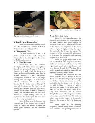
Figure 2.2 Microbalance with the SAW device in
the center
Biotin is used in research to test the
microbalance since it is representative of
biomolecules that can be measured on a
microbalance[6].
Another device that can be used as a
biosensor is a quartz crystal microbalance
(QCM). QCMs have larger electrodes, thus
better suited for finding changes in
frequencies. Though not a SAW device,
QCMs also utilize piezoelectricity and are a
suitable replacement for measurement
purposes. The major difference between the
SAW device and the QCM is that the SAW
device operates on transverse waves whereas
the QCM operates on longitudinal waves.
2.5 Microfabrication Processes and
Measurement Principles
2.5.1 Mask
Masks are tools to imprint the design
of the device onto the photoresist on the
aluminum conductor. The mask has a chrome
pattern of the SAW device on a glass substrate
as seen in Figure 2.3. A mask with defects can
result in a low yield of chips[4].
Figure 2.3 Glass mask with chrome pattern
2.5.2 Photolithography and Wet
Etching
Photolithography includes the process
of spin coating photoresist on to the substrate.
This procedure has to be done in a yellow-lit
room since the photoresist reacts to UV light.
The layer of photoresist applied by spin
coating reacts with the concentrated UV light
during exposure[7].
The process used to expose the
photoresist to the light is contact printing.
Contact printing involves the wafer touching
the mask to allow for correct pattern transfer
during exposure. Contact printing may be
susceptible to dust particles on the wafer that
can potentially damage the mask; therefore,
proper care must be taken during the mask to
substrate contact[4].
The developing stage removes the
photoresist that has been exposed to UV light
during exposure, leaving the unexposed
photoresist to remain on the substrate. After
using this resist to pattern the aluminum by
wet etching, the photoresist is left on the
wafer to prevent corrosion; this process is
called passivation.
The etch rate of the aluminum is not
only dependent on the concentration of
solutes but also on the temperature of the
solution, the agitation of wafers, and the
impurities or alloys in the film[4].](https://image.slidesharecdn.com/2142ebb7-c0f8-4580-ae2c-0ae145f7d634-160521180355/85/Surface-Acoustic-Wave-Devices-3-320.jpg)
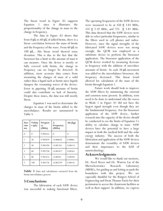
![4
2.5.3 Bandwidth and Operating
Frequency
The bandwidth is the optimal range of
frequencies that the device will allow. Any
frequency outside the bandwidth range will be
unlikely to resonate in the device. The
bandwidth is calculated by analyzing the
frequency values three decibels (dB) down
from the peak operating frequency – the
mode – and finding the width of the gap as
shown in Figure 2.4. The interval of 3 dB is
chosen since this marks the half power point -
the point at which the wave’s output power is
half that of its mid-band value.
The peak operating frequency is the
frequency associated with the wave that
experienced the most constructive
interference, as indicated by a high signal
strength. More than one operating frequency
can occur for each SAW filter. The resonance
of the waves results in a fundamental
frequency and additional harmonics, all of
which can be considered as multiple peak
operating frequencies.
Figure 2.4 The bandwidth of a wave between
frequency 1 and frequency 2
3 Microfabrication,
Measurements, and Biosensor
Application of SAW Devices
SAW devices and microbalances are
fabricated through a series of detailed steps
and tested.
3.1 Microfabrication of SAW
Devices in Cleanroom
Microfabrication includes electron
beam-physical vapor deposition,
photolithography, contact printing,
developing, and wet etching. This process was
done for five samples.
3.1.1 Cleaning and Electron Beam-
Physical Vapor Deposition
Cleaning of the quartz substrates was
done using acetone and methanol [8]. Next,
the wafer was rinsed with deionized water and
blown dry with nitrogen which quickly
evaporates any solvents or liquids on the
wafer. Nitrogen is used because it does not
cause the wafer to oxidize [9]. The wafer was
baked to dry and remove solvents. A film of
aluminum conductor was deposited on one
side of the quartz wafer by electron beam
physical vapor deposition [10], as shown in
Figure 3.1..
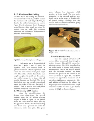
Figure 3.1 The samples of quartz substrate coated
with aluminum
3.1.2 Spin Coating
Spin coating began by placing the
sample in the middle of the spinner. A few
drops of photoresist (AZ 5124) were put onto
the center of the aluminum layer of the quartz
as seen in Figure 3.2 until the sample was
covered. To ensure the purity of the
photoresist, the tip of the dropper must not
touch the opening of the bottle nor the
sample. The substrate was then rotated at a
high speed in order to spread the coating](https://image.slidesharecdn.com/2142ebb7-c0f8-4580-ae2c-0ae145f7d634-160521180355/85/Surface-Acoustic-Wave-Devices-4-320.jpg)
![5
evenly by centrifugal force. Rotation was
done for 5 seconds at 500 rpm and then
subsequently for 40 seconds at 4,000 rpm.
After the spinning was done, the wafer was
soft baked to dry off any solvent from the spin
coating, improve the adhesion of the resist to
the wafer, and anneal the stresses put on the
wafer during spin coating[11].
Figure 3.2 Spinner with the aluminum-coated
substrate (Sample 1) and pink photoresist (AZ 5124)
For Sample 2, an extra layer of
photoresist was applied due to a spinner
error. After applying the photoresist to
Sample 2, the spinner started immediately at
4,000 rpm, a higher speed than intended. As a
result, the spinning was stopped and Sample 2
was reexamined; some of the photoresist was
no longer on the chip. Photoresist was
reapplied to Sample 2 and the correct
program was used to spin Sample 2.
3.1.3 Mask and Exposure
The samples were positioned on the
stage in order to maximize the number of
chips on the samples. Once the shadow
disappeared as the sample contacted the mask,
the UV light was turned on; exposure lasted
for 15 seconds.
For all samples, the shadow was
examined in order to ensure the wafer was
just touching the mask. As the wafer moved
closer to the mask, the shadow diminished.
3.1.4 Image Developing
The sample was then soaked in a
developer to remove the exposed photoresist
leaving behind the pattern as seen in Figure
3.3. The developer was AZ 1:1 and was
compatible with the AZ 5214 photoresist.
The amount of time in the developer varies
depending on the sample, but is usually
around one minute. The samples were
dipped in distilled water, then removed, and
then dipped once again. This method was used
to ensure that all the developer was off the
wafer. The wafer was then dried using high-
pressure nitrogen.
Figure 3.3 Samples after developing
As seen in Table 1, the samples were
in the developing solution twice before the
photoresist was removed. They had to be
developed for 30 sec, dried, and developed
for 30 sec again to observe the development
progress. Sample 2 needed more time during
the developing stage. Sample 2 was developed
for 1 minute and 6 seconds, with two rounds
of 30 seconds each and a third round of 6
seconds. This was likely because at the earlier
spinning step, the photoresist was re-applied.
Sample Developing Time/Sequence Etching
Time
1 30 sec + rinse + 30 sec + rinse =
60 sec total
11:50
2 30 sec + rinse + 30 sec + rinse +
6 sec + rinse= 66 sec total
20:07
3 30 sec + rinse + 30 sec + rinse =
60 sec total
25:01
4 30 sec + rinse + 30 sec + rinse =
60 sec total
9:00
5 30 sec + rinse + 30 sec + rinse=
60 sec total
10:42
Table 1 Developing and etching times](https://image.slidesharecdn.com/2142ebb7-c0f8-4580-ae2c-0ae145f7d634-160521180355/85/Surface-Acoustic-Wave-Devices-5-320.jpg)
![10
our gratitude to Robert Lorber for the
cleanroom technical support. We would also
like to thank The Governor’s School of
Engineering and its sponsors: Rutgers, The
State University of New Jersey, Morgan
Stanley, NJ Resources, South Jersey
Industries, PSE&G, and the GSET alumni and
community. Furthermore, we would like to
thank Jean Patrick Antoine, and all of the
counselors for giving us this opportunity. A
special thank you to Jeff Kowalski, our
Residential Teaching Associate, for always
being there for us and taking us to where we
need to be.
References
[1] "Highly Efficient Photovoltaic Energy
Conversion Using Surface Acoustic Waves in
Piezoelectric Semiconductors | University of
Maryland Energy Research Center." Highly
Efficient Photovoltaic Energy Conversion Using
Surface Acoustic Waves in Piezoelectric
Semiconductors | University of Maryland Energy
Research Center. N.p., n.d. Web. 24 July 2013.
<http://www.umerc.umd.edu/projects/sol
ar05>.
[2] “In NASA’s Sterile Areas, Plenty of
Robust Bacteria.” New York Times, 9.
October 2007.
[3] McFadden, Roger. "A Basic Introduction
to Clean Room." Coastwide Laboratories. N.p.,
n.d. Web. 5 July 2013.
<http://www.coastwidelabs.com/Technical
%20Articles/Cleaning%20the%20Cleanroom
.htm>.
[4] Ng, Kwok K. “Lithography and Etching.”
Semiconductor Device Technology. By Simon
M. Sze. N.p.: Wiley, 2005. 404-18. Print.
[5] Coon, Allan. "SAW Filter PCB Layout."
RFM. N.p., n.d. Web. 19 July
2013.
<http://www.rfm.com/products/apnotes/a
n42.pdf>.
[6] "What Is Biotin?" WiseGEEK. N.p., n.d.
Web. 19 July 2013.
<http://www.wisegeek.org/what-is-
biotin.htm>.
[7] "Photolithography." Photolithography.
N.p., n.d. Web. 05 July 2013.
<http://www.ece.gatech.edu/research/labs
/vc/theory/photolith.html>.
[8] "Cleaning Procedures for Class
Substrates." UCIRvine, n.d. Web. 5 July
2013.
<http://www.inrf.uci.edu/wordpress/wp-
content/uploads/sop-wet-cleaning-pro-for-
glass-substrates.pdf>.
[9] Downie, N. A. Industrial Gases. London:
Blackie Academic & Professional,
1997.Google Books. Web. 5 July 2013.
[10] "Electron Beam Physical Vapour
Deposition (EB-PVD)." Phoenix Scientific
Industries Ltd. N.p., n.d. Web. 04 July 2013.
<http://www.psiltd.co.uk/Products/Deposi
tionSystems/ElectronBeam/tabid/238/langu
age/en-GB/Default.aspx>.
[11] "Coating Quality and Spin
Coating." Materials Science and Engineering.
N.p., n.d. Web. 25 July 2013.](https://image.slidesharecdn.com/2142ebb7-c0f8-4580-ae2c-0ae145f7d634-160521180355/85/Surface-Acoustic-Wave-Devices-10-320.jpg)