Download as PDF, PPTX


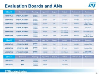
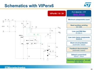
![VIPer06 / 16 /26
Main Features Pin description
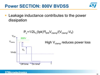
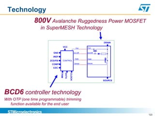
800V, avalanche rugged power MOSFET
PWM controller with drain current limit IDlim
Adjustable current limit,IDlim
Fixed frequency with Jittering
high performance for stand-by & efficiency
No need of auxiliary winding
Automatic auto restart after faults
Hysteretic thermal shutdown
Direct feedback for non isolated SMPS
Replacement of capacitive power supply
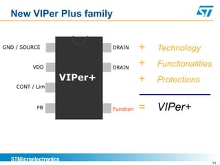
GND
Open loop protection
controller ground / power MOSFET Source
MAIN PARAMETERS
Power MOSFET CONTROLLER VDD
(SuperMESH)
Main parameters (BCD6S)
controller supply voltage / ICHARGE output current
Break down voltage [V] 800 LIM
Current limit set-up, IDlim .
RDSon [Ohm] 30 /24 / 7
FB
VDD [V] 9 ÷ 23 direct voltage feedback (in case of non isolated
SMPS)
FOSC [KHz] 30 or 60 or 115
COMP
Max IDlim [mA] 420 / 740 Compensation network.
RTHJ-A [°C/W] (1) 80 Current loop feedback in case of isolated SMPS
N.A.
POUT [W] @ 85-265 VAC 4 / 6 / 12
Not Available for user. (It can be connected to GND)
(1) Package SO16N, 100mm2 of Cu
N.C.
(2) Open Frame
Not Connected
62](https://image.slidesharecdn.com/stmicroelectronics-110913121934-phpapp02/85/Seminario-VIPerPlus-STMicroelectronics-62-320.jpg)

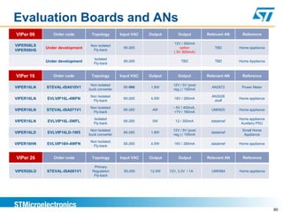
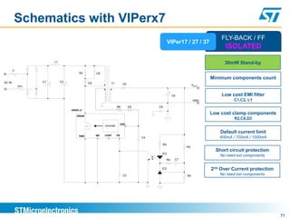
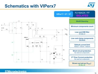
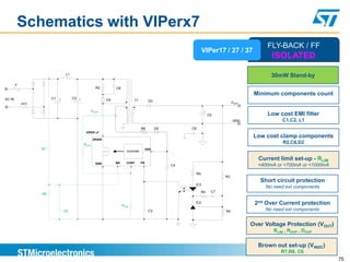
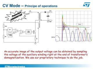
![VIPer17 / 27 / 37
Main Features Pin description
800V, avalanche rugged power MOSFET *
PWM controller with drain current limit, IDlim.
Adjustable current limit, IDlim
Fixed Frequency with Jittering
High performance for stand-by & efficiency
Integrated protections: OVP, OLP, high OCP
Automatic auto restart after fault
Hysteretic thermal shutdown
Brown-out: minimum input voltage is settable
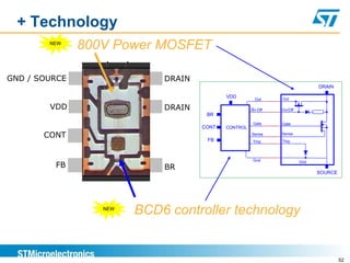
GND
Power MOSFET CONTROLLER controller ground / power MOSFET Source
MAIN PARAMETERS
Main parameters
(SuperMESH) (BCD6S) VDD
Break down voltage [V] 800 controller supply voltage / ICHARGE output current
CONT
RDSon [Ohm] 24 / 7 / 4.5
OVP set-up, IDLIM set-up.
VDD [V] 9 ÷ 23 FB
current loop feedback
FOSC [KHz] 60 or 115
BR *
Max IDlim [mA] 420 / 740 / 1050 brown out set-up
RTHJ-A [°C/W] (1) 50 N.A.
Not Available for user. (It can be connected to GND)
POUT [W] @ 85-265VAC 6 / 12 / 15
N.C.
(1) Package SO16N and 100mm2 of Cu
Not Connected
(2) Open Frame
* BR pin has the position 10 for VIPER17LD/HD (SO16N package)
70](https://image.slidesharecdn.com/stmicroelectronics-110913121934-phpapp02/85/Seminario-VIPerPlus-STMicroelectronics-70-320.jpg)


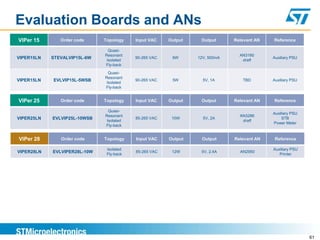
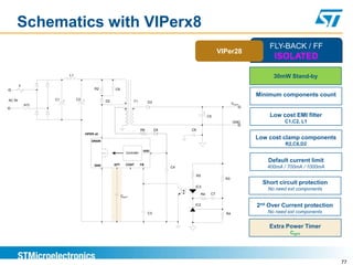
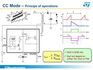
![VIPer28
Main Features Pin description
800V, avalanche rugged power MOSFET
PWM controller with drain current limit, IDlim.
Adjustable current limit, IDlim
Fixed Frequency with Jittering
High performance for stand-by & efficiency
Integrated protections: OVP, OLP, high OCP
Automatic auto restart after fault
Hysteretic thermal shutdown
Extra Power Management
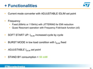
GND
Power MOSFET CONTROLLER controller ground / power MOSFET Source
MAIN PARAMETERS
Main parameters
(SuperMESH) (BCD6S) VDD
Break down voltage [V] 800 controller supply voltage / ICHARGE output current
COMP
RDSon [Ohm] 7
OVP set-up, IDLIM set-up.
VDD [V] 9 ÷ 23 FB
current loop feedback
FOSC [KHz] 60 or 115
EPT
Max IDlim [mA] 850 Extra Power Time set-up
RTHJ-A [°C/W] (1) 50 N.A.
Not Available for user. (It can be connected to GND)
POUT [W] @ 85-265VAC 12
N.C.
(1) Package SO16N and 100mm2 of Cu
Not Connected
(2) Open Frame
76](https://image.slidesharecdn.com/stmicroelectronics-110913121934-phpapp02/85/Seminario-VIPerPlus-STMicroelectronics-76-320.jpg)
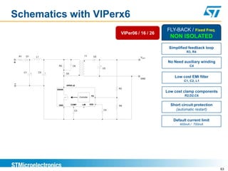
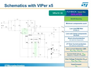
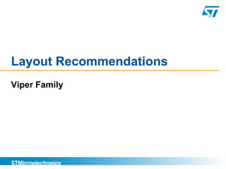
![VIPer15 / 25
Main Features Pin description
800V, avalanche rugged power MOSFET
Quasi-Resonant PWM controller with drain current
limit, IDlim.
Adjustable current limit, IDlim
Feed-Forward compensation
High performance for stand-by & efficiency
Integrated protections: OVP, OLP, high OCP
Automatic auto restart after fault
Hysteretic thermal shutdown
Brown-out: minimum input voltage is settable
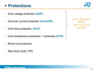
GND
MAIN PARAMETERS
Power MOSFET CONTROLLER controller ground / power MOSFET Source
(SuperMESH) (BCD6S)
Main parameters VDD
Break down voltage [V] 800 controller supply voltage / ICHARGE output current
ZCD
RDSon [Ohm] 24 / 7
Zero Current Detection, Feed-Forward set-up, OVP
VDD [V] 9 ÷ 23 set-up, IDlim set point.
up to 150 (L type) FB
FOSClim [KHz]
up to 225 (H type) Current loop feedback
Max IDlim [mA] 420 / 740 BR
RTHJ-A [°C/W] (1) 80
Brown out set-up
N.A.
POUT [W] @ 85-26 VAC 6 / 12
Not Available for user. (It can be connected to GND)
(1) Package SO16N, 100mm2 of Cu
N.C.
(2) Open Frame Not Connected
78](https://image.slidesharecdn.com/stmicroelectronics-110913121934-phpapp02/85/Seminario-VIPerPlus-STMicroelectronics-78-320.jpg)

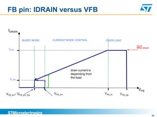
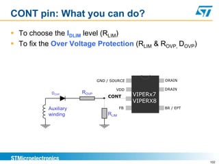
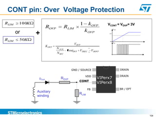
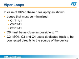
![CONT pin: IDLIM set point
Advantages :
Transformer optimization and accurate OLP.
Flexibility vs design changes
Flexibility vs different Projects (stock optimization)
1.2
(Normalized to IDLIM whitout RLIM)
1.0
GND / SOURCE DRAIN
0.8
VDD VIPERx7 DRAIN
IDLIM
0.6
CONT VIPERX8
0.4
FB BR / EPT 0.2
RLIM
0.0
0 20 40 60 80 100
RLIM [K ]
103](https://image.slidesharecdn.com/stmicroelectronics-110913121934-phpapp02/85/Seminario-VIPerPlus-STMicroelectronics-103-320.jpg)
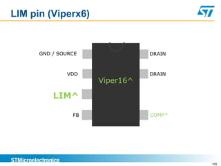
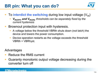
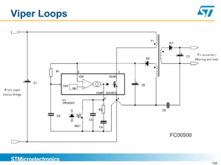
![LIM pin: What you can do?
To choose the IDLIM level (RLIM)
RLIM>100 kOhm or pin float:
IDlim default (typ, 400mA)
RLIM< 80 kOhm:
IDlim decreased continuously according to the current
sunk from the LIM pin 1.2
(Normalized to IDLIM whitout RLIM)
1.0
GND / SOURCE DRAIN
0.8
VDD DRAIN
IDLIM
0.6
LIM VIPERx6 0.4
FB 0.2
RLIM 0.0
0 20 40 60 80 100
RLIM [K ]
106](https://image.slidesharecdn.com/stmicroelectronics-110913121934-phpapp02/85/Seminario-VIPerPlus-STMicroelectronics-106-320.jpg)
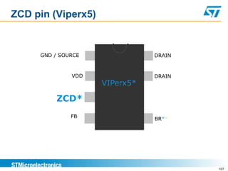
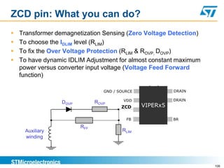
![ZCD pin: IDLIM set point
Advantages :
Transformer optimization and accurate OLP.
Flexibility vs design changes
Flexibility vs different Projects (stock optimization)
1.2
(Normalized to IDLIM whitout RLIM)
1.0
GND / SOURCE DRAIN
0.8
VDD DRAIN
IDLIM
0.6
ZCD VIPERx5
0.4
FB BR 0.2
RLIM
0.0
0 20 40 60 80 100
RLIM [K ]
109](https://image.slidesharecdn.com/stmicroelectronics-110913121934-phpapp02/85/Seminario-VIPerPlus-STMicroelectronics-109-320.jpg)

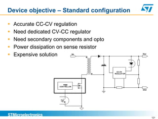
![Main electrical parameters – HVLED805
Main Features Pin description
800V, avalanche rugged power section
QR current-mode PWM controller in BCD6
technology SO16
Constant voltage and constant current output
regulation (CV/CC) with no optocoupler
Optimized for LED
High performance for stand-by & efficiency
Integrated protections: 2nd OCP, open loop
protection (brownout) OLP, high OCP SOURCE
Automatic auto restart after fault Power section Source
Vcc
Power MOSFET CONTROLLER
MAIN PARAMETERS controller supply voltage / ICHARGE output current
(SuperMESH) (BCD6S)
Main parameters GND
Break down voltage [V] 800
controller ground
RDSon [Ohm] 11 ILED
Current loop reference
VDD [V] 11.5 ÷ 23 DMG
Zero Current Detection
FOSC [KHz] Up to 166 kHz
COMP
Restart time during burst mode( 500us Compensation network
RTHJ-A [°C/W] (1) 80
DRAIN
Power section Drain
POUT [W] @ 85-265VAC 5
(1) Package SO16N and 100mm2 of Cu](https://image.slidesharecdn.com/stmicroelectronics-110913121934-phpapp02/85/Seminario-VIPerPlus-STMicroelectronics-124-320.jpg)
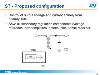
![Main electrical parameters – ALTAIR05T-800
Main Features Pin description
800V, avalanche rugged power section SOURCE 1 16 DRAIN
QR current-mode PWM controller in BCD6 SOURCE 2 15 DRAIN
technology SO16 Vcc 3 14 DRAIN
GND 4
Constant voltage and constant current output 13 DRAIN
IREF 5 12 N.C.
regulation (CV/CC) with no optocoupler
ZCD/FB 6 11 N.A.
High performance for stand-by & efficiency COMP 7 10 N.A.
Integrated protections: 2nd OCP, open loop CDC 8 9 N.A.
protection (brownout) OLP, high OCP
Automatic auto restart after fault SOURCE
Power section Source
Power MOSFET CONTROLLER Vcc
MAIN PARAMETERS
(SuperMESH) (BCD6S)
Main parameters controller supply voltage / ICHARGE output current
Break down voltage [V] 800 GND
controller ground
RDSon [Ohm] 11
IREF
VDD [V] 11.5 ÷ 23 Current loop reference
ZCD/FB
FOSC [KHz] Up to 166 kHz Zero Current Detection, Cvregulation, FF
compensation
Restart time during burst mode(1) 500us
COMP
RTHJ-A [°C/W] (2) 80 Compensation network
POUT [W] @ 85-265VAC 6 CDC
Cable Drop Cpmplensation
(1) Also 125us, 250us and 1ms available DRAIN
(2) Package SO16N and 100mm2 of Cu Power section Drain](https://image.slidesharecdn.com/stmicroelectronics-110913121934-phpapp02/85/Seminario-VIPerPlus-STMicroelectronics-125-320.jpg)
![Main electrical parameters – ALTAIR04-900
Main Features Pin description
900V, avalanche rugged power section SOURCE 1 16 DRAIN
QR current-mode PWM controller in BCD6 SOURCE 2 15 DRAIN
technology SO16 Vcc 3 14 DRAIN
Constant voltage and constant current output GND 4 13 DRAIN
IREF 5 12
regulation (CV/CC) with no optocoupler N.C.
ZCD/FB 6 11 N.C.
High performance for stand-by & efficiency
COMP 7 10 N.C.
Integrated protections: 2nd OCP, open loop N.C. 8 9 N.C.
protection (brownout) OLP, high OCP
Automatic auto restart after fault SOURCE
Power section Source
Power MOSFET CONTROLLER Vcc
MAIN PARAMETERS
(SuperMESH) (BCD6S)
Main parameters controller supply voltage / ICHARGE output current
Break down voltage [V] 900 GND
controller ground
RDSon [Ohm] 16
IREF
VDD [V] 11.5 ÷ 23 Current loop reference
ZCD/FB
FOSC [KHz] Up to 166 kHz Zero Current Detection, Cvregulation, FF
compensation
Restart time during burst mode(1) 500us
COMP
RTHJ-A [°C/W] (2) 50 Compensation network
POUT [W] @ 85-265VAC 5 DRAIN
Power section Drain
(1) Also 125us, 250us and 1ms available
(2) Package SO16N and 100mm2 of Cu](https://image.slidesharecdn.com/stmicroelectronics-110913121934-phpapp02/85/Seminario-VIPerPlus-STMicroelectronics-126-320.jpg)
![Typical load regulation cv/cc: high accuracy
6
High voltage accuracy 5
+/-2.5%
4
Output Voltage [V]
3
2 HV Startup is ON
1
0
0 200 400 600 800 1000 1200
Output Current [mA]
High current accuracy:
+/-5%
127](https://image.slidesharecdn.com/stmicroelectronics-110913121934-phpapp02/85/Seminario-VIPerPlus-STMicroelectronics-127-320.jpg)

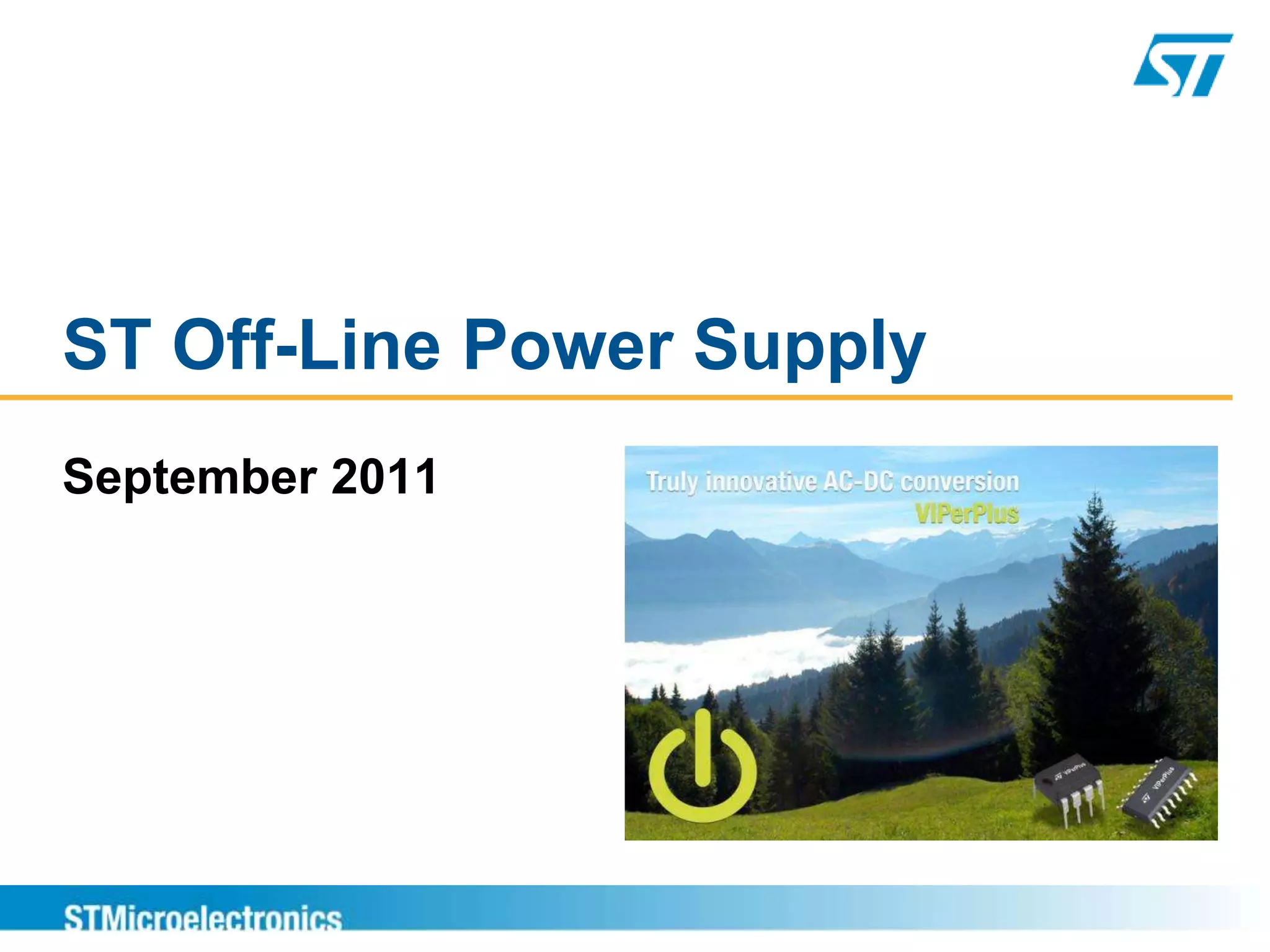
This document discusses ST's offline power supply products. It begins with an introduction to ST, including its market segments and major product lines. It then covers offline power supply configurations and topologies like SMPS. The document outlines ST's new VIPer+ family, including its roadmap and product details. It also discusses new products, magnetic components, and design tools and recommendations. The overall summary provides context about ST's offline power supply portfolio and upcoming products.


![RF Module Design - [Chapter 1] From Basics to RF Transceivers](https://cdn.slidesharecdn.com/ss_thumbnails/rfch1-150613070344-lva1-app6892-thumbnail.jpg?width=640&height=640&fit=bounds)
![RF Module Design - [Chapter 5] Low Noise Amplifier](https://cdn.slidesharecdn.com/ss_thumbnails/rfch5-150613070346-lva1-app6891-thumbnail.jpg?width=640&height=640&fit=bounds)


![RF Circuit Design - [Ch3-2] Power Waves and Power-Gain Expressions](https://cdn.slidesharecdn.com/ss_thumbnails/ch3-2-150613064404-lva1-app6891-thumbnail.jpg?width=640&height=640&fit=bounds)


