The Smart Pen project aims to digitize handwritten notes using a device that converts physical writing into editable digital text, leveraging hand-written optical character recognition (HW-OCR) technology. The system consists of hardware components like a mouse sensor and LED for coordinate detection, and software to process these coordinates into characters. This technology promises to streamline note-taking in meetings and can be integrated into various digital platforms to enhance accessibility and storage.
Introduction to Smart Pen that converts handwritten input to digital text using HW-OCR technology.
A description of the working prototype developed to read handwritten input and convert it to digital text.
Overview of the block diagram showing hardware (LED, USB supply, Mouse sensor) and software (HWOCR) components of the Smart Pen.
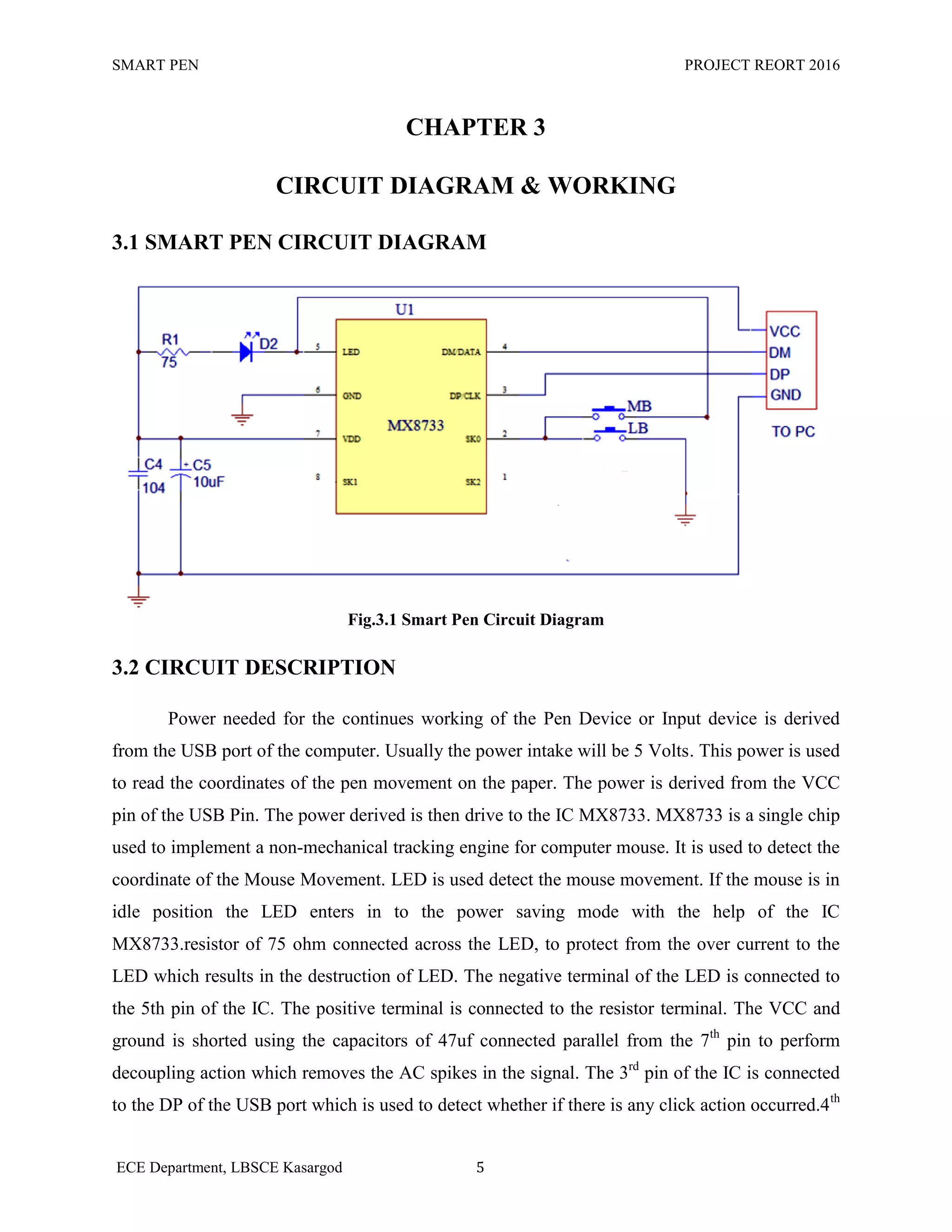
Circuit diagrams, components, and functionality of the Smart Pen including power supply and mouse sensor IC.
Explanation of resistors, capacitors, and LEDs used in the circuit, including their roles in ensuring performance.
Steps and considerations in PCB design including layout generation, fabrication, and soldering processes.
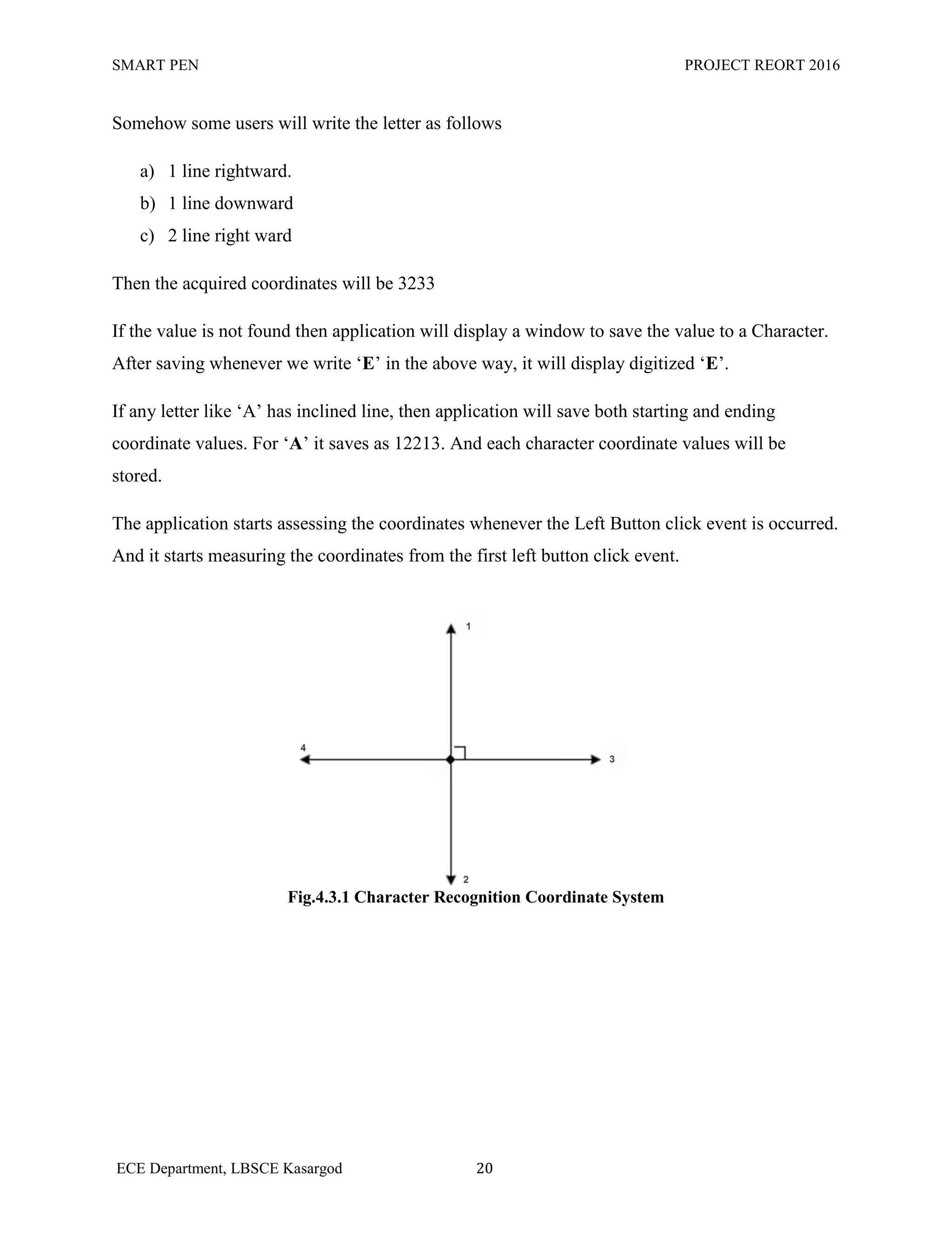
Description of the software functionality for character recognition using coordinates and customization options.
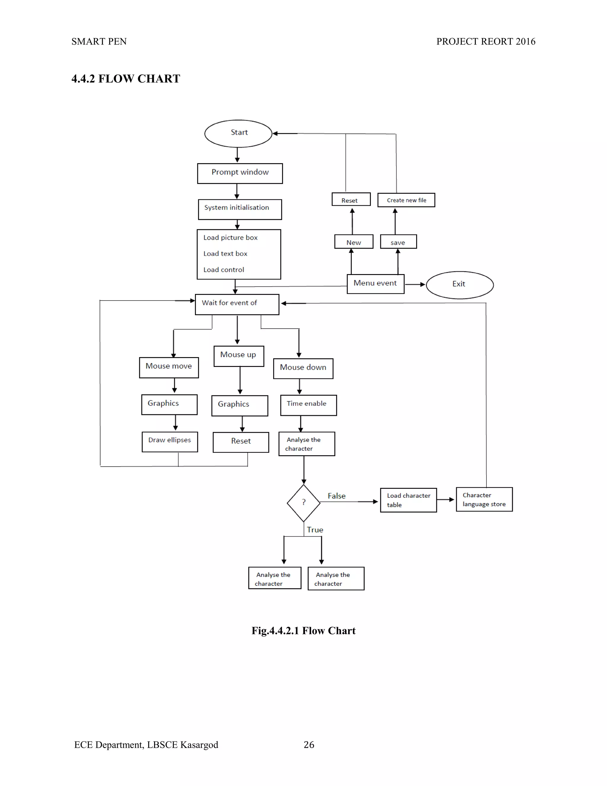
Algorithm steps and flow chart illustrating how the Smart Pen processes handwritten input for recognition.
Implementation results showing benefits of Smart Pen including ease of use, mobility, and applications in education.Conclusions and future prospects for Smart Pen technology in improving digital interaction and recognizing various scripts.
SMART PEN PROJECTREORT 2016
ECE Department, LBSCE Kasargod 1
CHAPTER 1
INTRODUCTION
In this busy life, we often have major meetings and business matters to consider. We need to
note all the situations which occurred in day to day life and those noted Information should be in
safe. We are living in a digital world and the format of living also is in digital form so that time
and money can be saved.
While we are attending a meeting. We might note all the discussions and those noted points are
to be converted to text format. It is difficult to type those items and to make a report. Here we are
introducing a device which converts hand written input to its digitized format automatically.
Smart pen is a new gen technology device used to digitize the hand written input. It is a pen
which is able to write in a paper and that information is stored as a text file in a computer and
that handwritten information is instantly converted in to editable text. It offers many features
such as portability, connectivity, ability to findable and ability to store.
It is based on the principle of HW-OCR (Hand Written Optical Character Recognition).It is an
attempt to link physical and digital information media and combine the best of both worlds in
one seamless experience. HWOCR is nothing but the technique which is used to convert
handwritten to digital text. If the pen has wireless connectivity, then recognized information can
be saved in cloud so that we can access the data to anywhere anytime. The received data can be
used for third party applications.
Here the hand written character is recognized by coordinate system. The coordinate system
consists of x and y coordinates. For each coordinate (both positive and Negative), a constant
values are assigned, that is 1 to 4 values in coordinate system. When we write a hand written
input, the Mouse Sensor IC Registers a Coordinate value and this Value is sent to the system for
processing over a input/output USB Channel. The System has a Database comprising Coordinate
Values for Each of the Character named Language Recognition File. The stored value and input
coordinate values are compared and if the values are matched. Then the Digital Character is
displayed at appropriate Fields. If the hand written character is failed to recognize, a character
recognition table will displayed. Where we can choose the proper character from the table and
the received coordinate values will be stored for that particular character. Hence whenever the
character written in the way, the character will be displayed correctly.
Smart Pen is Personalized Digital gadget constructed with the aim of reducing the Time and
Money to convert the physical handwritten input to the Digital Characters. If this Technologies
are wisely implemented more applications could be explored, like Small sized computers,
Mobiles, etc. 3D Designer tools. Hence the research and design area of this projects are Large
and wide.
2.
SMART PEN PROJECTREORT 2016
ECE Department, LBSCE Kasargod 2
In this Project we implement a fully working Prototype of the Smart Pen Described. That is read
a Handwritten input and to convert the Handwritten text to the Digital Character.
3.
SMART PEN PROJECTREORT 2016
ECE Department, LBSCE Kasargod 3
CHAPTER 2
BLOCK DIAGRAM
Fig.2.1 Block Diagram
2.1 BLOCK DIAGRAM DESCRIPTION
Block diagram for the Smart Pen is Described above. The Block diagram Smart pen has 2
portions. First one is hardware part and the second is the Software part. Which is the HWOCR
software to convert handwritten input to the Digital Character.
2.1.1 SMART PEN HARDWARE
It consist of LED ,Handwritten input, USB power supply, Mouse sensor IC, Coordinate
detection. Hand written input is written using the smart pen device . The internal structure of pen
consists of mouse sensor IC, LED, USB power supply. LED is mounted with a lens which is
used to focus the LED Light to the surface and to detect reflected light from the surface. The
power to drive the LED and sensor is driven from the USB port of the computer. The LED
moves as the pen moves to write the handwritten input, the sensor detect the reflected light from
4.
SMART PEN PROJECTREORT 2016
ECE Department, LBSCE Kasargod 4
the surface and calculates the X and Y coordinates. then this calculated coordinates are
transferred to the computer software section.
2.1.2 SMART PEN SOFTWARE
The calculated coordinates are transferred from digital pen hardware to computer to process the
coordinates using HW-OCR software in the computer; the coordinates are transferred to the
HWOCR program. The OCR program has a data base consisting of stored values for each and
every character. The coordinates received is compared with the stored values in the Data base. if
the input coordinates matches with the stored value a character in the database. Then the
digitized character is Displayed in the text box. If no such coordinate values are present in the
data base, Then a character Table is displayed. Where we can save the received coordinates for
the desired Character in the Character box.
5.
SMART PEN PROJECTREORT 2016
ECE Department, LBSCE Kasargod 5
CHAPTER 3
CIRCUIT DIAGRAM & WORKING
3.1 SMART PEN CIRCUIT DIAGRAM
Fig.3.1 Smart Pen Circuit Diagram
3.2 CIRCUIT DESCRIPTION
Power needed for the continues working of the Pen Device or Input device is derived
from the USB port of the computer. Usually the power intake will be 5 Volts. This power is used
to read the coordinates of the pen movement on the paper. The power is derived from the VCC
pin of the USB Pin. The power derived is then drive to the IC MX8733. MX8733 is a single chip
used to implement a non-mechanical tracking engine for computer mouse. It is used to detect the
coordinate of the Mouse Movement. LED is used detect the mouse movement. If the mouse is in
idle position the LED enters in to the power saving mode with the help of the IC
MX8733.resistor of 75 ohm connected across the LED, to protect from the over current to the
LED which results in the destruction of LED. The negative terminal of the LED is connected to
the 5th pin of the IC. The positive terminal is connected to the resistor terminal. The VCC and
ground is shorted using the capacitors of 47uf connected parallel from the 7th
pin to perform
decoupling action which removes the AC spikes in the signal. The 3rd
pin of the IC is connected
to the DP of the USB port which is used to detect whether if there is any click action occurred.4th
6.
SMART PEN PROJECTREORT 2016
ECE Department, LBSCE Kasargod 6
pin of IC is connected to the DM of the USB port. It is used to send the received data of
coordinates. Pin no. 2 of the IC is used to detect the Left mouse button. 6th
pin of the IC is
grounded. Pin no.1 and 2 are left unused.
The received co-ordinates are processed by the computer to read the co-ordinates of the
movement of the pen which is interrupted by the smart pen software (HW-OCR) to recognize the
character that has been written using smart pen device on the surface or Notebook, etc...
3.3 CIRCUIT COMPONENTS
The basic components of the smart pen device are
Power supply
USB port
Mouse sensor IC MX8733
Capacitors
Resistors
LED
3.3.1 POWER SUPPLY
The power supply is the most indispensable part of any Project. Power needed to drive
the USB device is derived from the USB port of the computer.it provides a regulated 5 Volt
output. The maximum output volt is 20v.
3.3.2 USB Port
Universal serial bus (USB) is the most successful interface in the history of PC. USB
technology is now very widely used as most popular connectivity interface standard, due to both
its flexibility and simplicity for the end user. Connecting USB peripherals to a computer has
becoming significantly easier. The USB connector is remarkably simple having just four main
connections for the data and power. In addition to this, it is also possible to use extender cables.
The maximum available length for an individual cable is 5 meter and this allows the USB data
acquisition module to be located remotely from the computer. Like all connectors those used for
USB have Male and Female versions to ensure that device are Mated in the correct direction.
7.
SMART PEN PROJECTREORT 2016
ECE Department, LBSCE Kasargod 7
3.3.2.1 Typical USB connector
Remote devices have what is termed an upstream connection to a host. In turn hosts have
downstream connections to remote devices. Upstream and downstream connectors are not
mechanically interchangeable. This ensure that they can only be connected in the required
direction there by eliminating the possibility of issues such as illegal loopback connections at the
hubs like upstream ports being connected to another downstream port. Until recently there was
no peer to peer functionality.
3.3.2.2 USB connector types
As the concept of USB has developed so too have the connector‟s .data transfer speeds
have risen and the requirement for smaller connectors has increased. As a result there are 7 USB
connector Types: Type A, Type B, mini-B, micro B and micro AB. type A and B have four pins
within the connector, mini and micro A and B connectors have 5 pin.
3.3.2.3 USB type A and B PinOuts/Connections
The basic USB pinouts for the connectors are given in the table below. apart from USB
connector pinouts, the table also gives wire colours used within the cables.
Pin Name Colour Code Description
1 VCC Red +5 VDD
2 D- White Data -
3 D+ Green Data +
4 GND Black Ground
Table.3.3.2.4.1 USB Pinouts
8.
SMART PEN PROJECTREORT 2016
ECE Department, LBSCE Kasargod 8
Fig.3.3.2.4.1 USB Pinout
3.3.3 MOUSE SENSOR IC MX8733
Fig.3.3.3.1 MX8733 IC
The MX8733 chip is a low cost single chip optical mouse solution used to implement a
non-mechanical tracking engine for computer mice.it is based on optical navigation technology
with USB/PS2 combo MCU bundled. This measures change in position optically acquiring
sequential surface images/frames and mathematically determining direction and magnitude of
moment. single chip optical mouse sensor provides a complete and compact mouse solution,
There are no moving parts, Precision Optical Alignment is not required, few outside components
use and facility high volume assembly.it is a true crystal-less and ultra-low cost solution.
It has several features. Some of the Features are
9.
SMART PEN PROJECTREORT 2016
ECE Department, LBSCE Kasargod 9
Optical navigation technology
Low cost and Powerful solution for PS/2 and low speed USB combo mouse
Microsoft 3d IntelliMouse and IBM PS/2 mouse compatible
Crystal-less
5 Volt power supply
Low EMI radiation
Resolution 800CPI
Supports 3D (X,Y,Z) inputs
Fig.3.3.3.2 MX8733 Pinout Diagram
Pin No Symbol I/O Function
1 SK2 I/O Z axis Input 2
2 SK0 I/O Left button input and Middle button input
3 DP/CLK I/O USB D+ / PS2 CLK
4 DM/DATA I/O USB D- / PS2 DATA
5 LED O LED control (Sink Current) and key scan
6 GND P GND
7 VDD P 5V Power Input
8 SK1 I/O Z axis Input 1 and Right button input
Table.3.3.3.2 MX8733 Pinout
10.
SMART PEN PROJECTREORT 2016
ECE Department, LBSCE Kasargod 10
3.3.4 CAPACITORS
Fig.3.3.4.1 Capacitor
A capacitor is a two-terminal, electrical component. Along with resistors and inductors,
they are one of the most fundamental passive components we use. What makes capacitors special
is their ability to store energy; they‟re like a fully charged electric battery. Caps, as we usually
refer to them, have all sorts of critical applications in circuits. Common applications include
local energy storage. Capacitance is its Unit. Not all capacitors are created equal. Each capacitor
is built to have a specific amount of capacitance. The capacitance of a capacitor tells you how
much charge it can store, more capacitance means more capacity to store charge. The standard
unit of capacitance is called the farad, which is abbreviated F. It turns out that a farad is a lot of
capacitance, even 0.001F (1 milli farad – 1mF) is a big capacitor. Usually we‟ll see capacitors
rated in the Pico- (10-12) to microfarad (10-6) range.
3.3.5 RESISTORS
Fig.3.3.5.1 Resistors
Resistors are the most commonly used component in electronics and their purpose is to create
specified values of current and voltage in a circuit. The unit for measuring resistance is the
OHM. (The Greek letter Ω - called Omega). Higher resistance values are represented by „k‟
(kilo-ohms) and M (Mega ohms). For example, 120 000 Ω is represented as 120k, while
1200000 Ω is represented as 1MΩ. The dot is generally omitted as it can easily be lost in the
11.
SMART PEN PROJECTREORT 2016
ECE Department, LBSCE Kasargod 11
printing process. In some circuit diagrams, a value such as 8 or 120 represents a resistance in
ohms. Another common practice is to use the letter E for resistance in ohms. The letter R can
also be Resistor Markings.
Resistance value is marked on the resistor body. Most resistors have 4 bands. The first
two bands provide the numbers for the resistance and the third band provides the number of
zeros. The fourth band indicates the tolerance. Tolerance values of 5%, 2%, and 1% are used.
The following table shows the Color Code used to identify resistor values.
COLOR DIGIT MULTIPLIER TOLERANCE TC
Silver x 0.01 W ±10%
Gold x 0.1 W ±5%
Black 0 x 1 W
Brown 1 x 10 W ±1% ±100*10-6
/K
Red 2 x 100 W ±2% ±50*10-6
/K
Orange 3 x 1 kW ±15*10-6
/K
Yellow 4 x 10 Kw ±25*10-6
/K
Green 5 x 100 kW ±0.5%
Blue 6 x 1 MW ±0.25% ±10*10-6
/K
Violet 7 x 10 MW ±0.1% ±5*10-6
/K
Grey 8 x 100 MW
White 9 x 1 GW ±1*10-6
/K
Table 3.3.5.1 Resistor Color Codes
3.3.6 LIGHT EMITING DIODE (LED)
Fig.3.3.6.1 LED
12.
SMART PEN PROJECTREORT 2016
ECE Department, LBSCE Kasargod 12
LEDs emit light when energy levels change in the semiconductor diode. This shift in
energy generates photons, some of which are emitted as light. The specific wavelength of the
light depends on the difference in energy levels as well as the type of semiconductor material
used to form the LED chip. Solid-state design allows LEDs to withstand shock, vibration,
frequent switching (electrical on and off shock) and environmental (mechanical shocks)
extremes without compromising their famous long life typically 100,000 hours or more.
Typically, Red, Green, and Blue LEDs emit a band of spectrum, depending on the
material system. The white LED draws much attention for the illumination devices. Comparing
the LED illumination with the conventional illumination such as fluorescent lamps and
incandescent bulbs, the LED illumination has many advantages such as high efficiency,
environment-friendly manufacturing, design flexibility, long lifetime, and better spectrum
performance. The LED which we are using for the Smart Pen Project is of colour Red.
The basic LED consists of a semiconductor diode chip mounted in the reflector cup of a
lead frame that is connected to electrical (wire bond) wires, and then encased in a solid epoxy
lens. The architecture of LED is shown in Fig.
Fig.3.3.6.2 LED Architecture
13.
SMART PEN PROJECTREORT 2016
ECE Department, LBSCE Kasargod 13
3.4 THE PCB LAYOUT
3.4.1 PCB DESIGN
Design of printed circuit board (PCB) can be considered as the last step in electronic circuit
design as well as the first step in production. It plays important role in the performance and reliability
of electronic circuits, the productivity of the PCB‟s its assembling, and its service ability depends on
design. All these factors get reflected in a piece of electronic equipment. It is clear that task of PCB
design is not very simple or always straight forward. The schematic is follower by layout generation.
Layout design is the stage where engineering capacity combined with creativity is the governing
inputs.
3.4.2 ELECTRONIC DESIGN AUTOMATION TOOLS
Most product testing is being done is done with the help of computer programs. The term
Electronic Design Automation (EDA) is being used to describe the use of these tools. With the
help of advanced powerful computing systems and interactive software tools and development of
electronic circuits has undergone automation. Thus the software and hardware tools, which
enables this automation includes PCB designing, IC design, circuit simulation etc. These tools
help us in such a way that we can draw the circuit; test the functioning of the circuit in response
to test inputs in simulation software.
After successfully simulation we can get the PCB art work done by replacing the routing
software. The design automation tool used here is ORCAD.
3.4.3 PCB DESIGN PROCEDURES
The PCB designing procedure consists of following steps:
3.4.3.1 DRAWING THE CIRCUIT SCHEMATIC
Drawing of circuit is done through ORCAD CAPTURE. It includes many libraries with
thousands of component symbols. We can select the required symbol from the library and place it in
the schematic page. After placing the component symbols, we can complete the interconnection
using wire or bus control.
The next step is to assign part reference. Each component has to be assigned footprint or PCB
pattern name. The footprint gives the actual size physical representation of components on the PCB
artwork. The component symbol and foot symbol should correspond in all respects.
14.
SMART PEN PROJECTREORT 2016
ECE Department, LBSCE Kasargod 14
3.4.3.2 DESIGN RULE CHECK AND NET LIST CREATION
After the circuit schematic is completed with all required information such as part reference
and footprints, the design rule check can be used for checking errors in the design. It will check for
duplicate symbols, overlapped lines and dangling lines.
After the schematic design file passes the DRC check, it is processed by a program called an
electric rule checker (ERC) that checks for writing errors. The final operation to be done before
starting PCB artwork is the net list creation.
A net list creation of the components and interconnection along with other information such
as foot prints, track width etc. A net list software or tool can take the circuit schematic as input and
generate net list. The net list can be used as an information source for the remaining stages.
3.4.3.3 CREATING THE PCB ARTWORK
In automatic design, the net list obtained from the previous stage is used for getting the
required foot print and interconnections. The software used for the PCB artwork design in the
ORCAD LAYOUT.
3.4.3.4 PCB FABRICATION
You need to generate a positive (copper black) UV translucent art work film. You will never get a
good board without good art work, so it is important to get the best possible quality at this stage. The
most important thing is to get a clear sharp image with a very solid opaque black. Art work is done
using ORCAD software. It is absolutely essential that your PCB software prints holes in the middle
of pads, which will act as center marks when drilling. It is virtually impossible to accurately hand-
drill boards without these holes. If you are looking to buy PCB software at any cost level and want to
do hand-prototyping of boards before production, check that this facility is available when defining
pad and line shapes, the minimum size recommended (through-linking holes) for reliable result is 50
mil, assuming 0.8mm drill size; 1 mil=(1/1000)th
of an inch. You can go smaller drill sizes, but
through linking will be harder. 65mil round or square pads for normal components.
ICs, with 0.8 mm hole, will allow a 12.5mil, down to 10mil if you really need to. Center-to-
center spacing of 12.5 mil tracks should be 25 mil-slightly less may be possible if your printer can
manage it. Take care to preserve the correct diagonal track-track spacing on mitered corners; grid is
25 mil and track width 12.5mil. The art work must be printed such that the printed side is in contact
with PCB surface when exposing, to avoid blurred edges. In practice, this means that if you design
15.
SMART PEN PROJECTREORT 2016
ECE Department, LBSCE Kasargod 15
the board as seen from the component side, the bottom (solder side) layer should be printed the
„correct‟ way round, and top side of the double-sided board must be printed mirrored.
3.4.3.5 ETCHING
Ferric chloride etchant is a messy stuff, but easily available and cheaper than most
alternatives. It attacks any metal including stainless steel. So when setting up a PCB etching area, use
a plastic or ceramic sink, with plastic fitting and screws wherever possible, and seal any metal screws
with silicon. Copper water pipes may be splashed or dripped-on, so sleeve or cover them in plastic;
heat-shrink sleeve is great if you are installing new pipes. Fume extraction is not normally required,
although a cover over the tank or tray when not in use is a good idea. You should always use the hex
hydrate type of ferric chloride, which should be dissolved in warm water until saturation. Adding a
teaspoon of table salt helps to make the etchant clearer for easier inspection. Avoid anhydrous ferric
chloride. It creates a lot of heat when dissolved. So always add the powder very slowly to water; do
not add water to the powder, and use gloves and safety glasses. The solution made from anhydrous
ferric chloride doesn‟t etch at all, so you need to add a small amount of hydrochloric acid and leave it
for a day or two. Always take extreme care to avoid splashing when dissolving either type of ferric
chloride, acid tends to clump together and you often get big chunks coming out of the container and
splashing into the solution. It can damage eyes and permanently stain clothing. If you are making
PCBs in a professional environment where time is money you should get a heated bubble-etch tank.
With fresh hot ferric chloride, the PCB will etch in well under 5 minutes. Fast etching produces
better edge-quality and consistent line widths. If you aren‟t using a bubble tank, you need to agitate
frequently to ensure even etching. Warm the etchant by putting the etching tray inside a larger tray
filled with boiling water.
3.4.3.6 DRILLING
If you have fiber glass (FR4) board, you must use tungsten carbide drill bits. Fiberglass eats
normal high-speed steel (HSS) bits very rapidly, although HSS drills are alright for older larger sizes
(> 2mm). Carbide drill bits are available as straight-shank or thick-shank. In straight shank, the hole
bit is the diameter of the hole, and in thick shank, a standard size (typically about 3.5 mm) shank
tapers down to the hole size.
The straight-shank drills are usually preferred because they break less easily and are usually
cheaper. The longer thin section provides more flexibility. Small drills for PCB use usually come
with either a set of collets of various sizes or a three-jaw chuck. Sometimes the 3-jaw chuck is an
16.
SMART PEN PROJECTREORT 2016
ECE Department, LBSCE Kasargod 16
optional extra and is worth getting for the time it saves on changing collets. For accuracy, however,
3-jaw chucks are not brilliant, and small drill sizes below 1 mm quickly formed grooves in the jaws,
preventing good grip. Below 1 mm, you should use collets, and buy a few extra of the smallest ones;
keeping one collect per drill size as using a larger drill in a collet will open it out and it no longer
grips smaller drills well. You need a good strong light on the board when drilling, to ensure accuracy.
A dichroic halogen lamp, under run at 9V to reduce brightness, can be mounted on a microphone
gooseneck for easy positioning. It can be useful to raise the working surface above 15 cm above the
normal desk height for more comfortable viewing. Dust extraction is nice, but not essential and
occasional blow does the trick! A foot-pedal control to switch the drill “off” and “on” is very
convenient, especially when frequently changing bits. Avoid hole sizes less than 0.8 mm unless you
really need them. When making two identical boards, drill them both together to save time. To do
this, carefully drill a 0.8 mm whole in the pad near each corner of each of the two boards, getting the
center as accurately as possible. For larger boards, drill a hole near the center of each side as well.
Lay the boards on the top of each other and insert a 0.8 mm track pin in two opposite corners, using
the pins as pegs to line the PCBs up. Squeeze or hammer the pins into boards, and then into the
remaining holes. The two PCBs are now „nailed‟ together accurately and can be drilled together.
3.4.3.7 SOLDERING
Soldering is the joining together of two metals to give physical bonding and good electrical
conductivity. It is used primarily in electrical and electronic circuitry. Solder is a combination of
metals, which are solid at normal room temperatures and become liquid between 180 and 200 degree
Celsius. Solder bonds well to various metals, and extremely well to copper. Soldering is a necessary
skill you need to learn to successfully build electronics circuits. To solder you need a soldering iron.
A modern basic electrical soldering iron consists of a heating element, a soldering bit (often called a
tip), a handle and a power cord.
The heating element can be either a resistance wire wound around a ceramic tube, or a thick
film resistance element printed on to a ceramic base. The element is then insulated and placed into a
metal tube for strength and protection. This is then thermally insulated from the handle. The heating
element of soldering iron usually reaches temperatures of around 370 to 400 degree Celsius (higher
than need to melt the solder). The strength or power of a soldering iron is usually expressed in watts.
Irons generally used in electronics are typically in the range of 12 to 25 watts. Higher powered iron
will not run hotter. Most irons are available in a variety of voltages; 12V, 24V, 115V and 230V are
most popular.
17.
SMART PEN PROJECTREORT 2016
ECE Department, LBSCE Kasargod 17
Today most laboratories and repair shops use soldering irons, which operate at 24V. You
should always use this low voltage where possible, as it is much safer. For advanced soldering work,
you will need a soldering iron with temperature control. In this type of soldering irons, the
temperature may be usually set between 200 and 450 degree Celsius.
Many temperature control soldering iron designed for electronics have a power rating of
around 40 to 50 watt. They will heat fast and give enough power for operation, but are mechanically
small.
You will occasionally see gas-powered soldering irons which use butane rather than the main
electrical supply to operate. They have a catalytic element which once warmed up, continues to glow
hot when gas passes over them. Gas powered soldering irons are designed for occasional „on the
spot‟ used for quick repairs, rather than for main stream construction or for assembly work.
Currently, the best commonly available, workable, and safe solder alloy is 63/37. That is,
63% lead, 37% tin. It is also known as eutectic solder. Its most desirable characteristic is that it solids
(„pasty‟) state, and its liquid state occur at the same temperature -361 degree 22 Fahrenheit. The
combination of 63% lead and 37% tin melts at the lowest possible temperature. Nowadays there is
tendency to move to use lead free solders, but it will take years until they catch on normal soldering
work. Lead free solders are nowadays available, but they are generally more expensive or harder to
work on than traditional solders that they have lead in them.
The metals involved are not the only things to consider in a solder. Flux is vital to a good
solder joint. Flux is an aggressive chemical that removes oxide and impurities from the parts to be
soldered. The chemical reactions at the point(s) of connection must take place for the metal to fuse.
RMA type flux (Rosin Mildly Active) is the least corrosive of the readily available materials, and
provides an adequate oxide. In electronics, a 60/40 fixed core solder is used. This consists of 60%
lead and 40% tin, with flux cores added to the length of solder.
There are certain safety measures which you should keep in mind when soldering. The tin
material used in soldering contains dangerous substances like lead (40-60% of typical soldering tins
are lead and lead is poisonous). Also the various fumes from the soldering flux can be dangerous.
While it is true that lead does not vaporize at the temperature at which soldering is typically done.
When soldering, keep the room well ventilated and use a small fan or fume trap. A proper
fume trap of a fan will keep the most pollution away from your face. Professional electronic
workshops use expensive fume extraction systems to protect their workers. Those fume extraction
devices have a special filter which filters out the dangerous fumes. If you can connect a duct to the
output from the trap to the outside, that would be great.
18.
SMART PEN PROJECTREORT 2016
ECE Department, LBSCE Kasargod 18
Always wash hands prior to smoking, eating, drinking or going to the bathroom. When you
handle soldering tin, your hands will pick up lead, which needs to be washed out from it before it
gets to your body. Do not eat, drink or smoke while working with soldering iron. Do not place cups,
glasses or a plate of food near your working area.
3.5 PCB LAYOUT
Fig.3.4.1 PCB Layout
19.
SMART PEN PROJECTREORT 2016
ECE Department, LBSCE Kasargod 19
CHAPTER 4
HW-OCR PROGRAM
4.1 SMART PEN APPLICATION
The received coordinates are entered to the computer as the mouse coordinates. Using a
Programming language like C#, the coordinates are read from the Operating system and used for
character recognition. Character recognition is performed by storing constant values for each
Character. Whenever the coordinates received from the OS is matched with the previously stored
value its displays that particular Character. The important feature of the software is that it can be
personalized according to the user using the Smart Pen. Since all the humans have different style
of Handwritten. So whenever the received coordinates are not matched with the previously
stored value, the software shows a window which will help the user to select the desired
character. The value is then stored in the memory with the Desired character. In addition to this
the Application can support the third party applications. That is the recognized character can be
write in to third party applications like MS Word, Note Pad etc.
4.2 RECOGNITION LOGIC
It have 4 coordinates facing 4 directions. Each direction has unique values
Upward = 1
Downward = 2
Right = 3
Left = 4
If the character E represents 2333. Whenever the user write the Letter E on the Pad as
a) One line downward
b) 3 lines right ward.
The program read the coordinate as 2333. And it searches for the value 2333 in the previously
saved list. If the value is found then the Character representing the values is displayed that is „E‟.
20.
SMART PEN PROJECTREORT 2016
ECE Department, LBSCE Kasargod 20
Somehow some users will write the letter as follows
a) 1 line rightward.
b) 1 line downward
c) 2 line right ward
Then the acquired coordinates will be 3233
If the value is not found then application will display a window to save the value to a Character.
After saving whenever we write „E‟ in the above way, it will display digitized „E‟.
If any letter like „A‟ has inclined line, then application will save both starting and ending
coordinate values. For „A‟ it saves as 12213. And each character coordinate values will be
stored.
The application starts assessing the coordinates whenever the Left Button click event is occurred.
And it starts measuring the coordinates from the first left button click event.
Fig.4.3.1 Character Recognition Coordinate System
21.
SMART PEN PROJECTREORT 2016
ECE Department, LBSCE Kasargod 21
4.3 TOOLS USED & SMART PEN SOFWRE WALKTHROUGH
The software used for implement the SMART PEN APPLICCATION is Visual C#. C# is
an elegant and type-safe object-oriented language that enables developers to build a variety of
secure and robust applications that run on the .NET Framework. You can use C# to create
Windows client applications, XML Web services, distributed components, client-server
applications, database applications, and much, much more. Visual C# provides an advanced code
editor, convenient user interface designers, integrated debugger, and many other tools to make it
easier to develop applications based on the C# language and the .NET Framework.
C# syntax is highly expressive, yet it is also simple and easy to learn. The curly-brace
syntax of C# will be instantly recognizable to anyone familiar with C, C++ or Java. Developers
who know any of these languages are typically able to begin to work productively in C# within a
very short time. C# syntax simplifies many of the complexities of C++ and provides powerful
features such as null value types, enumerations, delegates, lambda expressions and direct
memory access, which are not found in Java. C# supports generic methods and types, which
provide increased type safety and performance, and iterators, which enable implementers of
collection classes to define custom iteration behaviors that are simple to use by client code.
Language-Integrated Query (LINQ) expressions make the strongly-typed query a first-class
language construct.
As an object-oriented language, C# supports the concepts of encapsulation, inheritance,
and polymorphism. All variables and methods, including the Main method, the application's
entry point, are encapsulated within class definitions. A class may inherit directly from one
parent class, but it may implement any number of interfaces. Methods that override virtual
methods in a parent class require the override keyword as a way to avoid accidental redefinition.
In C#, a structure is like a lightweight class; it is a stack-allocated type that can implement
interfaces but does not support inheritance.
22.
SMART PEN PROJECTREORT 2016
ECE Department, LBSCE Kasargod 22
Fig.4.3.1 The C# Start screen
On running the source code following window appears with a voice welcoming to the Smart Pen
Application. And other voice command to open the voice recognition file, which have the
previously saved values for the Characters.
Fig.4.3.2 Home Screen of the SMART PEN Application
23.
SMART PEN PROJECTREORT 2016
ECE Department, LBSCE Kasargod 23
After selecting the language recognition file, we will have 2 windows. A picture box where the
movement of the pen is shown real time. The picture will shows only for few time less than a
second and only after the left button click event is occurred. And Text Box which shows the
Recognized Text in the Box.
Fig.4.3.3 Text Recognition Process
When a non-recognized coordinates are acquired then a second window will appear to save the
coordinates for the required Character.
Fig.4.3.4 Save New Character Values
24.
SMART PEN PROJECTREORT 2016
ECE Department, LBSCE Kasargod 24
If we want to send the recognized text to a third party application. There is a button named
“Load”, press the Load button. It will list all the running applications in the dropdown menu list.
Select application and check the box with the option “send to the application” .The recognized
text will pass to the Application.
Fig 4.3.5 Send to the 3rd
Party Application
4.4 ALGORITHM & FLOW CHART
4.4.1 ALGORITHM
STEP 1: Start
STEP 2 : Show Prompt window to select Language Recognition File
STEP 3 : System initialization
STEP 4 : Load Picture box, Text Box, and Control buttons
STEP 5 : Wait for an Event else go to step 20
STEP 6 : If Mouse Move is detected go to Step 7 else go to Step 9
STEP 7 : initialize the Graphics module
STEP 8 : Draw Ellipses and go to step 1
25.
SMART PEN PROJECTREORT 2016
ECE Department, LBSCE Kasargod 25
STEP 9 : If Mouse up event is occurred go to step 10 else go to 12
STEP 10 : Initialize the Graphics module
STEP 11 : Reset the Picture box
STEP 12 : Mouse down event is occurred
STEP 13 : Enables the Timer to read the coordinates
STEP 14 : Analyze the character coordinates
STEP 15 : If coordinate match with the stored value go to step 16 or else go to step 18
STEP 16 : Display the recognized character in the Text Box. Or else go to step 17
STEP 17 : Send to process (Third party Application)
STEP 18 : Load the Character Table
STEP 19 : Store the value for new Character.
STEP 20 : Menu Event Occurred
STEP 21 : New button event occurred or else go to 23
STEP 22 : Reset the Text Box and Picture Box
STEP 23 : Save event is Occurred
STEP 24 : Create new Text File
STEP 25 : Exit
SMART PEN PROJECTREORT 2016
ECE Department, LBSCE Kasargod 27
CHAPTER 5
RESULT AND ANALYSIS
in this project we implement Smart Pen to Digitize the Handwritten Input using an Simple
Software using Hand Written – Optical Character Recognition Algorithm (HW-OCR).
The proto type of the Proposed system is Implemented
Fig.5.1 SMART PEN Device
28.
SMART PEN PROJECTREORT 2016
ECE Department, LBSCE Kasargod 28
5.1 ADVANTAGES
SMART PEN is bridge between the Physical and Digital world. Where the Handwritten
input is directly converted to the Digitized text with in no time or Real time. There are numerous
advantages of the Smart Pen can be easily seen. Some of the important advantages are Listed
Below.
5.1.1 EASY TO USE CUSTOMIZABLE MULTIPURPOSE PEN
Smart pen is a Customizable Digital Device, it can be customize according to the users.
The trained data or previously stored can vary person to person. Hence the user can set or use
His own Writing Style. It can replace the Mouse Peripheral to the computer, since the both
device do the same method to recognize the Coordinates.
5.1.2 SIMPLE USER INTERFACE
The Smart Pen application has the Simple User Interface. Not much training required for
user to familiarize the Application. Hence it is very easy to use.
5.1.3 MOBILITY
The size of the device is very small, as long as a pen. Hence it Can be used as standard
pen and can carry anywhere without stressing mind to carry it. It provides greater mobility if the
connectivity is wireless.
5.1.4 THIRD PARTY APPLICATION CAN BE HOSTED
Smart Pen Application supports the Third party applications to use the Recognized text as
their input. It is great advantage for the Businessmen, students, etc..They‟re work can be directly
saved in the desired format and applications.
5.1.5 INEXPENSIVE, FAST AND RELIABLE
5.2 LIMITATIONS
The Major Limitation of this Technology are,
5.2.1 COMPLICATION IN HANDWRITTEN RECOGNITION
Hand written Recognition Algorithm is very Much Complicated algorithm. The
characters are recognized by storing coordinate values for and every Character. Hence the
character only displayed only when the acquired character coordinates matches with the stored
29.
SMART PEN PROJECTREORT 2016
ECE Department, LBSCE Kasargod 29
character coordinates. The coordinates of each character will change person to person and for
different handwriting styles.
5.2.2 NO TEMPLATES OR SOPHISTICATED FORMAT ARE AVAILABLE
Since the hand writing is different to person to person, while designing the SMART PEN
Application no Templates or sophisticated format for Handwritten are available. Hence
Programmer set the values according to His Handwriting style. Later when it reaches to
customer, if the handwriting is different from the Programmers, the customer has to reconfigure
the Language recognition file according to his style. It is time consuming and extreme care
should be taken while setting this coordinate values.
5.2.3 AWARENESS REQUIRES
Even though the SMART PEN Application has Minimal User Interface, awareness required to
customers for on how to set the new character coordinate values, how to use Third Party
application with the Application.
5.2.4 THIRD PARTY USE IS RISKY
As Mentioned earlier the SMART PEN is a personalized device, that is the character values are
set according to that particular User. So whenever a third party uses the device, it may not
generate the desired results owing to different handwritten styles.
5.3 APPLICATIONS
The proposed system has Numerous Applications. Some of the applications are Listed Below,
5.3.1 CAN BE USED AS A PERSONAL ASSISTANT DEVICE
SMART PEN can be used as a personal assistant device for Managers, CEOs, and IT
Professionals. Since their productive thoughts, or programming can be saved in to computer
without typing each and every character. Sometimes may be saved to cloud services. If such
connectivity‟s are implemented on the device.
5.3.2 AS INPUT DEVICE
Smart pen is multipurpose digital device, which can used as character input device or Mouse to
the computer or Character input devices for the Physical World
5.3.3 MINIMAL COMPUTING EXPERIENCE
Smart Pen can be used as Both Character and Mouse input to a computer, hence the need of a
Keyboard and separate Mouse can be avoided.
30.
SMART PEN PROJECTREORT 2016
ECE Department, LBSCE Kasargod 30
5.3.4 EDUCATIONAL PURPOSES
The device can be used in the field of education. Students can take notes using this pen, the
digitized character representation will be stored in the attached SD Card. So the need of carrying
note book each and every subject is not necessary. And losing of the materials also will not
occur.
31.
SMART PEN PROJECTREORT 2016
ECE Department, LBSCE Kasargod 31
CHAPTER 6
CONCLUSION
This project is an attempt to Link both the Physical and Digital world linking handwritten input
to the Computers, Mobile phones. To Prepare Text files, Send Emails, Set reminders, etc. If the
technology implemented wisely the future computers will be minimalized by removing the
separate Input Devices like Keyboard and Mouse. And problems regarding the static input
devices can be ignored. The technology can be elaborated to Recognizes different Languages and
scripts. And designers can use draw 3D pictures by implementing more features to this SMART
PEN. So the research field are wide and large. More feature can incorporated and using
miniature circuitry to make it a Necessary personal gadget device like mobile phones of this
Generation.
6.1 FUTURE SCOPE
The Future scope this Promising Technology is Listed Below,
More Connectivity option can be Incorporated with device, which enables the user to
connect various Devices wirelessly and even the recognized text can be made to store in
the Cloud Storage. Which helps to access the Texts anywhere anytime.
Numerous Language and Script Recognition can be implemented, hence user can write in
any language
By implementing 3D Graphics in to the PEN, Instead of using Complex soft wares, the
designer can put his heart down in to the computer. It saves a lot of time and No
compromise required in the creativity.
And there are so many fields where smart pens applications can be extended.
32.
SMART PEN PROJECTREORT 2016
ECE Department, LBSCE Kasargod 32
REFERENCES
“Quickies : Intelligent Sticky Notes” Journal Paper by Pranav Mistry and Pattie Maes
from MIT Media Lab
Hay Stack Project.
http://groups.csail.mit.edu/haystack/
www.YouTube.com – TED Talk by Pranav Mistry
C# 5.0 Programmers Reference by Rod Stephens
www.wikipedia.org – Quickies and Hay stack Project