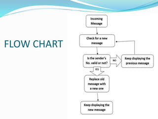
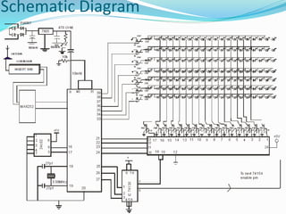
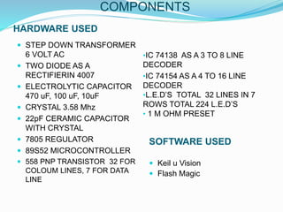
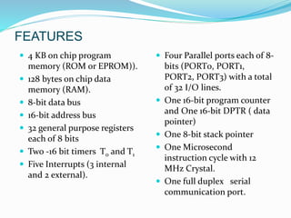
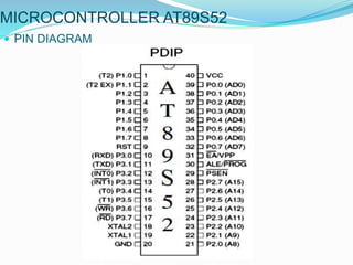
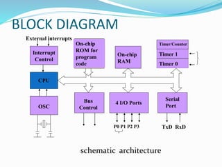
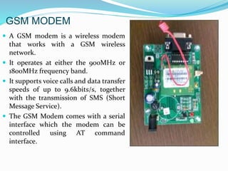
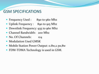
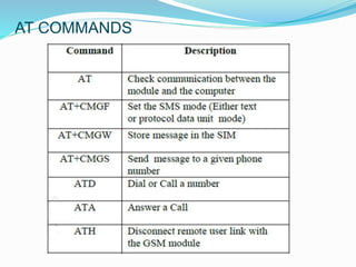
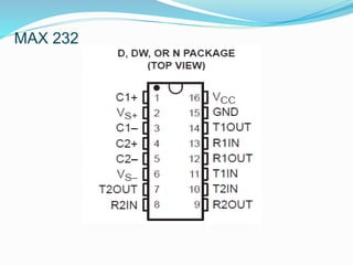
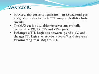
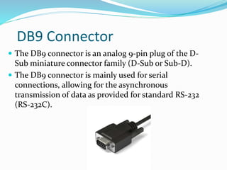
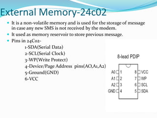
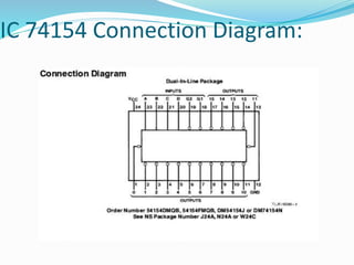
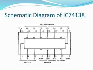
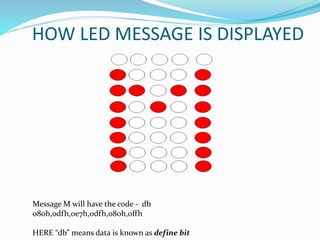
Submitted By:
Swarnim Maurya
Bharat Bhagtani
Vishu Jain
(DR. K.N. Modi Institute of Engg. & Tech. , Modinagar,
Ghaziabad)
CONTENTS
1. Project Idea
2. Introduction
3. Working Principle
4. Flow Chart
5. Schematic Diagram
6. Components used
a) AT89S52
b)GSM Modem
c)MX232 and DB9 Connector
d)DECODER IC’s
i- IC 74154
ii- IC74138
e)EEPROM (IC 24C02)
7- LED MATRIX
8- APPLICATION
9- CONCLUSION
10- REFERENCES
PROJECT IDEA:
 Notice Board is primary thing in any institution or organization or
public utility places like bus stations, railway stations and parks. But
sticking various notices day-to-day is a difficult process.
 A separate person is required to take care of this notices display. This
project deals about an advanced hi-tech wireless notice board.
 The project is built around a micro controller which provides all the
functionality of the display and wireless control. Display is obtained
on LED
 The advantage of this project being low cost and low power
consumption.
INTRODUCTION
 It presents an SMS based notice board incorporating the
widely used GSM to facilitate the communication of
displaying message on notice board via user’s mobile phone.
 SIM300 GSM modem with a SIM card is interfaced to the
ports of the microcontroller with the help of AT commands.
 SIM300 is duly interfaced through a level shifter IC MAX32
to the microcontroller. The messaged is thus fetched into the
microcontroller.
 It is further displayed on an electronic notice board which
equipped with LED display interfaced to microprocessor
powered by a regulated power supply from mains supply of
230 volts ac.
WORKING PRINCIPLE
 The GSM Modem is first properly initialized and then it
checks for modem connectivity. The program is written in
microcontroller to perform this task.
 After that user has to send SMS to GSM modem and
message contents are finally displayed on the LED matrix.
The microcontroller used in this project is Atmel 89S52.
 The data is sent to microcontroller through MAX232
interface. MAX232 acts as logic level shifter IC. It means, it
converts TTL Logic Level to RS-232 and vise versa.
FLOW CHART
Schematic Diagram
COMPONENTS
HARDWARE USED
•IC 74138 AS A 3 TO 8 LINE
DECODER
•IC 74154 AS A 4 TO 16 LINE
DECODER
•L.E.D’S TOTAL 32 LINES IN 7
ROWS TOTAL 224 L.E.D’S
• 1 M OHM PRESET
 STEP DOWN TRANSFORMER
6 VOLT AC
 TWO DIODE AS A
RECTIFIERIN 4007
 ELECTROLYTIC CAPACITOR
470 uF, 100 uF, 10uF
 CRYSTAL 3.58 Mhz
 22pF CERAMIC CAPACITOR
WITH CRYSTAL
 7805 REGULATOR
 89S52 MICROCONTROLLER
 558 PNP TRANSISTOR 32 FOR
COLOUM LINES, 7 FOR DATA
LINE
SOFTWARE USED
 Keil u Vision
 Flash Magic
89S52 Microcontroller
 Microcontroller is a small computer on a single
integrated circuit containing a processor core,
memory and programmable I/O peripherals.
 The 89S52 microcontroller has Harvard
architecture with RISC (Reduced Instruction Set
Computer) concept.
 The 89S52RB2/RC2/RD2 device contains a non-
volatile 16kB/32kB/64kB Flash program memory
that is both parallel programmable and serial In-
System and In-Application Programmable.
 89S52 has 8-bit ALU which can perform all the 8-
bit arithmetic and logical operations in one
machine cycle. The ALU is associated with two
registers A & B special function registers.
FEATURES
 4 KB on chip program
memory (ROM or EPROM)).
 128 bytes on chip data
memory (RAM).
 8-bit data bus
 16-bit address bus
 32 general purpose registers
each of 8 bits
 Two -16 bit timers T0 and T1
 Five Interrupts (3 internal
and 2 external).
 Four Parallel ports each of 8-
bits (PORT0, PORT1,
PORT2, PORT3) with a total
of 32 I/O lines.
 One 16-bit program counter
and One 16-bit DPTR ( data
pointer)
 One 8-bit stack pointer
 One Microsecond
instruction cycle with 12
MHz Crystal.
 One full duplex serial
communication port.
MICROCONTROLLER AT89S52
 PIN DIAGRAM
BLOCK DIAGRAM
schematic architecture
CPU
On-chip
RAM
On-chip
ROM for
program
code
4 I/O Ports
Timer 0
Serial
PortOSC
Interrupt
Control
External interrupts
Timer 1
Timer/Counter
Bus
Control
TxD RxDP0 P1 P2 P3
GSM MODEM
 A GSM modem is a wireless modem
that works with a GSM wireless
network.
 It operates at either the 900MHz or
1800MHz frequency band.
 It supports voice calls and data transfer
speeds of up to 9.6kbits/s, together
with the transmission of SMS (Short
Message Service).
 The GSM Modem comes with a serial
interface which the modem can be
controlled using AT command
interface.
GSM SPECIFICATIONS
 Frequency Used : 890 to 960 Mhz
 Uplink Frequency : 890 to 915 Mhz
 Downlink Frequency: 935 to 960 Mhz
 Channel Bandwidth: 200 Mhz
 No. Of Channels: 124
 Modulation Used GMSK
 Mobile Station Power Output: 0.8w,2.5w,8w
 FDM-TDMA Technology is used in GSM.
AT COMMANDS
MAX 232
MAX 232 IC
• MAX 232 that converts signals from an RS-232 serial port
to signals suitable for use in TTL compatible digital logic
circuits.
• The MAX 232 is a dual driver/receiver and typically
converts the RX, TX CTS and RTS signals.
• It changes a TTL Logic 0 to between +3 and +15 V, and
changes TTL logic 1 to between -3 to -15V, and vice versa
for converting from RS232 to TTL.
DB9 Connector
 The DB9 connector is an analog 9-pin plug of the D-
Sub miniature connector family (D-Sub or Sub-D).
 The DB9 connector is mainly used for serial
connections, allowing for the asynchronous
transmission of data as provided for standard RS-232
(RS-232C).
External Memory-24c02
 It is a non-volatile memory and is used for the storage of message
in case any new SMS is not received by the modem.
 It used as memory reservoir to store previous message.
 Pins in 24C02-
1-SDA(Serial Data)
2-SCL(Serial Clock)
3-WP(Write Protect)
4-Device/Page Address pins(AO,A1,A2)
5-Ground(GND)
6-VCC
Power Supply
 In this project firstly we use one step down transformer. Step down
transformer step down the voltage from 220 volt Ac to 12 volt Ac.
 This AC voltage is further converted into DC with the help of
rectifier circuit. In rectifier circuit we use TWO diode.
 All the diodes are arranges as a bridge rectifier circuit. Output of
this rectifier is pulsating Dc. To convert this pulsating DC into
smooth dc we use one capacitor as a filter components.
 Capacitor converts the pulsating Dc into smooth DC with the help
of its charging and discharging effect.
 Output of the rectifier is now regulated with the help of IC
regulator circuit . We use 7805 regulator then its means its is 5 volt
regulator and if we use 7808 regulator then its means that it is 8
volt regulator circuit.
 In this project we use 5 volt dc regulated power supply for the
complete circuit. Separate 9 volt dc power supply is used for the
relay coil
Schematic View of Power Supply
Design
Transfor
mer
Diode for
Rectification
Capacitor
LED
Voltage
Regulator
IC
IC 74154 (4-16 line demultiplexer):
Each or these 4-line-to-16-line decoders utilizes TTL circuitry to decode four
binary-coded inputs into one of sixteen
mutually exclusive outputs when both the strobe inputs, G1 and G2, are
low. The demultiplexing function is performed
by using the 4 input lines to address the output line, passing data from
one of the strobe inputs with the other strobe
input low. When either strobe input is high, all outputs are high. These
demultiplexers are ideally suited for implementing
high-performance memory decoders. All inputs are buffered and input
clamping diodes are provided to minimize
transmission-line effects and thereby simplify system design.
IC 74154 Connection Diagram:
IC 74138
The DM74LS138 decodes one-of-eight lines, based upon the conditions at the three binary
select inputs and the three enable inputs.
Two active-low and one active-high enable inputs reduce the need for external gates or
inverters when expanding.
An enable input can be used as a data input for demultiplexing applications.
The DM74LS139 comprises two separate two-line-to-fourline
decoders in a single package. The active-low enable
input can be used as a data line in demultiplexing applications.
Features
 Designed specifically for high speed:
 Memory decoders
 Data transmission systems
 n DM74LS138 3-to-8-line decoders incorporates 3 enable
 inputs to simplify cascading and/or data reception
 n DM74LS139 contains two fully independent 2-to-4-line
decoders/demultiplex
 DM74LS138 21 ns
 n Typical power dissipation
 DM74LS138 -32 mW power
Schematic Diagram of IC74138
HOW LED MESSAGE IS DISPLAYED
Message M will have the code - db
080h,0dfh,0e7h,0dfh,080h,0ffh
HERE “db” means data is known as define bit
APPLICATIONS
• The Campus Display System is aimed at the colleges and
universities for displaying day-to-day information continuously
or at regular intervals during working hours. Display devices can
be setup at various places in the campus.
• Being GSM-based system, it offers flexibility to display flash
news or announcements faster than a programmable system.
• GSM-based campus display system can also be used at other
public places like schools, hospitals, railway stations, gardens
etc. without affecting the surrounding environment.
CONCLUSION
 The display boards are one of the major communications
medium for mass media.
 Local language can be added as a variation in this project. This
can be achieved by using graphics and other decoding
techniques. Also we realize that this project saves time, energy
and hence environment. Cost of printing and photocopying is
also reduced as information can be given to a large number of
people from our fingertips.
 Thus we can conclude that this project is just a start, an idea to
make use of GSM in communications to a next level.
References
• “The 8051 Microcontroller and Embedded
Systems” by Muhammad Ali Mazidi and Janice
Gillispie Mazidi, Pearson Education.
• ATMEL 89S52 Data sheets
 www.fadooengineers.com
 www.wikipedia.org
Thank You!!!

Smart LED Notice Board

  • 1.
    Submitted By: Swarnim Maurya BharatBhagtani Vishu Jain (DR. K.N. Modi Institute of Engg. & Tech. , Modinagar, Ghaziabad)
  • 2.
    CONTENTS 1. Project Idea 2.Introduction 3. Working Principle 4. Flow Chart 5. Schematic Diagram 6. Components used a) AT89S52 b)GSM Modem c)MX232 and DB9 Connector d)DECODER IC’s i- IC 74154 ii- IC74138 e)EEPROM (IC 24C02) 7- LED MATRIX 8- APPLICATION 9- CONCLUSION 10- REFERENCES
  • 3.
    PROJECT IDEA:  NoticeBoard is primary thing in any institution or organization or public utility places like bus stations, railway stations and parks. But sticking various notices day-to-day is a difficult process.  A separate person is required to take care of this notices display. This project deals about an advanced hi-tech wireless notice board.  The project is built around a micro controller which provides all the functionality of the display and wireless control. Display is obtained on LED  The advantage of this project being low cost and low power consumption.
  • 4.
    INTRODUCTION  It presentsan SMS based notice board incorporating the widely used GSM to facilitate the communication of displaying message on notice board via user’s mobile phone.  SIM300 GSM modem with a SIM card is interfaced to the ports of the microcontroller with the help of AT commands.  SIM300 is duly interfaced through a level shifter IC MAX32 to the microcontroller. The messaged is thus fetched into the microcontroller.  It is further displayed on an electronic notice board which equipped with LED display interfaced to microprocessor powered by a regulated power supply from mains supply of 230 volts ac.
  • 5.
    WORKING PRINCIPLE  TheGSM Modem is first properly initialized and then it checks for modem connectivity. The program is written in microcontroller to perform this task.  After that user has to send SMS to GSM modem and message contents are finally displayed on the LED matrix. The microcontroller used in this project is Atmel 89S52.  The data is sent to microcontroller through MAX232 interface. MAX232 acts as logic level shifter IC. It means, it converts TTL Logic Level to RS-232 and vise versa.
  • 6.
  • 7.
  • 8.
    COMPONENTS HARDWARE USED •IC 74138AS A 3 TO 8 LINE DECODER •IC 74154 AS A 4 TO 16 LINE DECODER •L.E.D’S TOTAL 32 LINES IN 7 ROWS TOTAL 224 L.E.D’S • 1 M OHM PRESET  STEP DOWN TRANSFORMER 6 VOLT AC  TWO DIODE AS A RECTIFIERIN 4007  ELECTROLYTIC CAPACITOR 470 uF, 100 uF, 10uF  CRYSTAL 3.58 Mhz  22pF CERAMIC CAPACITOR WITH CRYSTAL  7805 REGULATOR  89S52 MICROCONTROLLER  558 PNP TRANSISTOR 32 FOR COLOUM LINES, 7 FOR DATA LINE SOFTWARE USED  Keil u Vision  Flash Magic
  • 9.
    89S52 Microcontroller  Microcontrolleris a small computer on a single integrated circuit containing a processor core, memory and programmable I/O peripherals.  The 89S52 microcontroller has Harvard architecture with RISC (Reduced Instruction Set Computer) concept.  The 89S52RB2/RC2/RD2 device contains a non- volatile 16kB/32kB/64kB Flash program memory that is both parallel programmable and serial In- System and In-Application Programmable.  89S52 has 8-bit ALU which can perform all the 8- bit arithmetic and logical operations in one machine cycle. The ALU is associated with two registers A & B special function registers.
  • 10.
    FEATURES  4 KBon chip program memory (ROM or EPROM)).  128 bytes on chip data memory (RAM).  8-bit data bus  16-bit address bus  32 general purpose registers each of 8 bits  Two -16 bit timers T0 and T1  Five Interrupts (3 internal and 2 external).  Four Parallel ports each of 8- bits (PORT0, PORT1, PORT2, PORT3) with a total of 32 I/O lines.  One 16-bit program counter and One 16-bit DPTR ( data pointer)  One 8-bit stack pointer  One Microsecond instruction cycle with 12 MHz Crystal.  One full duplex serial communication port.
  • 11.
  • 12.
    BLOCK DIAGRAM schematic architecture CPU On-chip RAM On-chip ROMfor program code 4 I/O Ports Timer 0 Serial PortOSC Interrupt Control External interrupts Timer 1 Timer/Counter Bus Control TxD RxDP0 P1 P2 P3
  • 13.
    GSM MODEM  AGSM modem is a wireless modem that works with a GSM wireless network.  It operates at either the 900MHz or 1800MHz frequency band.  It supports voice calls and data transfer speeds of up to 9.6kbits/s, together with the transmission of SMS (Short Message Service).  The GSM Modem comes with a serial interface which the modem can be controlled using AT command interface.
  • 14.
    GSM SPECIFICATIONS  FrequencyUsed : 890 to 960 Mhz  Uplink Frequency : 890 to 915 Mhz  Downlink Frequency: 935 to 960 Mhz  Channel Bandwidth: 200 Mhz  No. Of Channels: 124  Modulation Used GMSK  Mobile Station Power Output: 0.8w,2.5w,8w  FDM-TDMA Technology is used in GSM.
  • 15.
  • 16.
  • 17.
    MAX 232 IC •MAX 232 that converts signals from an RS-232 serial port to signals suitable for use in TTL compatible digital logic circuits. • The MAX 232 is a dual driver/receiver and typically converts the RX, TX CTS and RTS signals. • It changes a TTL Logic 0 to between +3 and +15 V, and changes TTL logic 1 to between -3 to -15V, and vice versa for converting from RS232 to TTL.
  • 18.
    DB9 Connector  TheDB9 connector is an analog 9-pin plug of the D- Sub miniature connector family (D-Sub or Sub-D).  The DB9 connector is mainly used for serial connections, allowing for the asynchronous transmission of data as provided for standard RS-232 (RS-232C).
  • 19.
    External Memory-24c02  Itis a non-volatile memory and is used for the storage of message in case any new SMS is not received by the modem.  It used as memory reservoir to store previous message.  Pins in 24C02- 1-SDA(Serial Data) 2-SCL(Serial Clock) 3-WP(Write Protect) 4-Device/Page Address pins(AO,A1,A2) 5-Ground(GND) 6-VCC
  • 20.
    Power Supply  Inthis project firstly we use one step down transformer. Step down transformer step down the voltage from 220 volt Ac to 12 volt Ac.  This AC voltage is further converted into DC with the help of rectifier circuit. In rectifier circuit we use TWO diode.  All the diodes are arranges as a bridge rectifier circuit. Output of this rectifier is pulsating Dc. To convert this pulsating DC into smooth dc we use one capacitor as a filter components.  Capacitor converts the pulsating Dc into smooth DC with the help of its charging and discharging effect.  Output of the rectifier is now regulated with the help of IC regulator circuit . We use 7805 regulator then its means its is 5 volt regulator and if we use 7808 regulator then its means that it is 8 volt regulator circuit.  In this project we use 5 volt dc regulated power supply for the complete circuit. Separate 9 volt dc power supply is used for the relay coil
  • 21.
    Schematic View ofPower Supply Design Transfor mer Diode for Rectification Capacitor LED Voltage Regulator IC
  • 22.
    IC 74154 (4-16line demultiplexer): Each or these 4-line-to-16-line decoders utilizes TTL circuitry to decode four binary-coded inputs into one of sixteen mutually exclusive outputs when both the strobe inputs, G1 and G2, are low. The demultiplexing function is performed by using the 4 input lines to address the output line, passing data from one of the strobe inputs with the other strobe input low. When either strobe input is high, all outputs are high. These demultiplexers are ideally suited for implementing high-performance memory decoders. All inputs are buffered and input clamping diodes are provided to minimize transmission-line effects and thereby simplify system design.
  • 23.
  • 24.
    IC 74138 The DM74LS138decodes one-of-eight lines, based upon the conditions at the three binary select inputs and the three enable inputs. Two active-low and one active-high enable inputs reduce the need for external gates or inverters when expanding. An enable input can be used as a data input for demultiplexing applications. The DM74LS139 comprises two separate two-line-to-fourline decoders in a single package. The active-low enable input can be used as a data line in demultiplexing applications.
  • 25.
    Features  Designed specificallyfor high speed:  Memory decoders  Data transmission systems  n DM74LS138 3-to-8-line decoders incorporates 3 enable  inputs to simplify cascading and/or data reception  n DM74LS139 contains two fully independent 2-to-4-line decoders/demultiplex  DM74LS138 21 ns  n Typical power dissipation  DM74LS138 -32 mW power
  • 26.
  • 27.
    HOW LED MESSAGEIS DISPLAYED Message M will have the code - db 080h,0dfh,0e7h,0dfh,080h,0ffh HERE “db” means data is known as define bit
  • 28.
    APPLICATIONS • The CampusDisplay System is aimed at the colleges and universities for displaying day-to-day information continuously or at regular intervals during working hours. Display devices can be setup at various places in the campus. • Being GSM-based system, it offers flexibility to display flash news or announcements faster than a programmable system. • GSM-based campus display system can also be used at other public places like schools, hospitals, railway stations, gardens etc. without affecting the surrounding environment.
  • 29.
    CONCLUSION  The displayboards are one of the major communications medium for mass media.  Local language can be added as a variation in this project. This can be achieved by using graphics and other decoding techniques. Also we realize that this project saves time, energy and hence environment. Cost of printing and photocopying is also reduced as information can be given to a large number of people from our fingertips.  Thus we can conclude that this project is just a start, an idea to make use of GSM in communications to a next level.
  • 30.
    References • “The 8051Microcontroller and Embedded Systems” by Muhammad Ali Mazidi and Janice Gillispie Mazidi, Pearson Education. • ATMEL 89S52 Data sheets  www.fadooengineers.com  www.wikipedia.org
  • 31.