Download as PDF, PPTX
![Systems with COM [dB]
Structures #1 2.9 (FAIL)
Structures #2 3.65 (PASS)
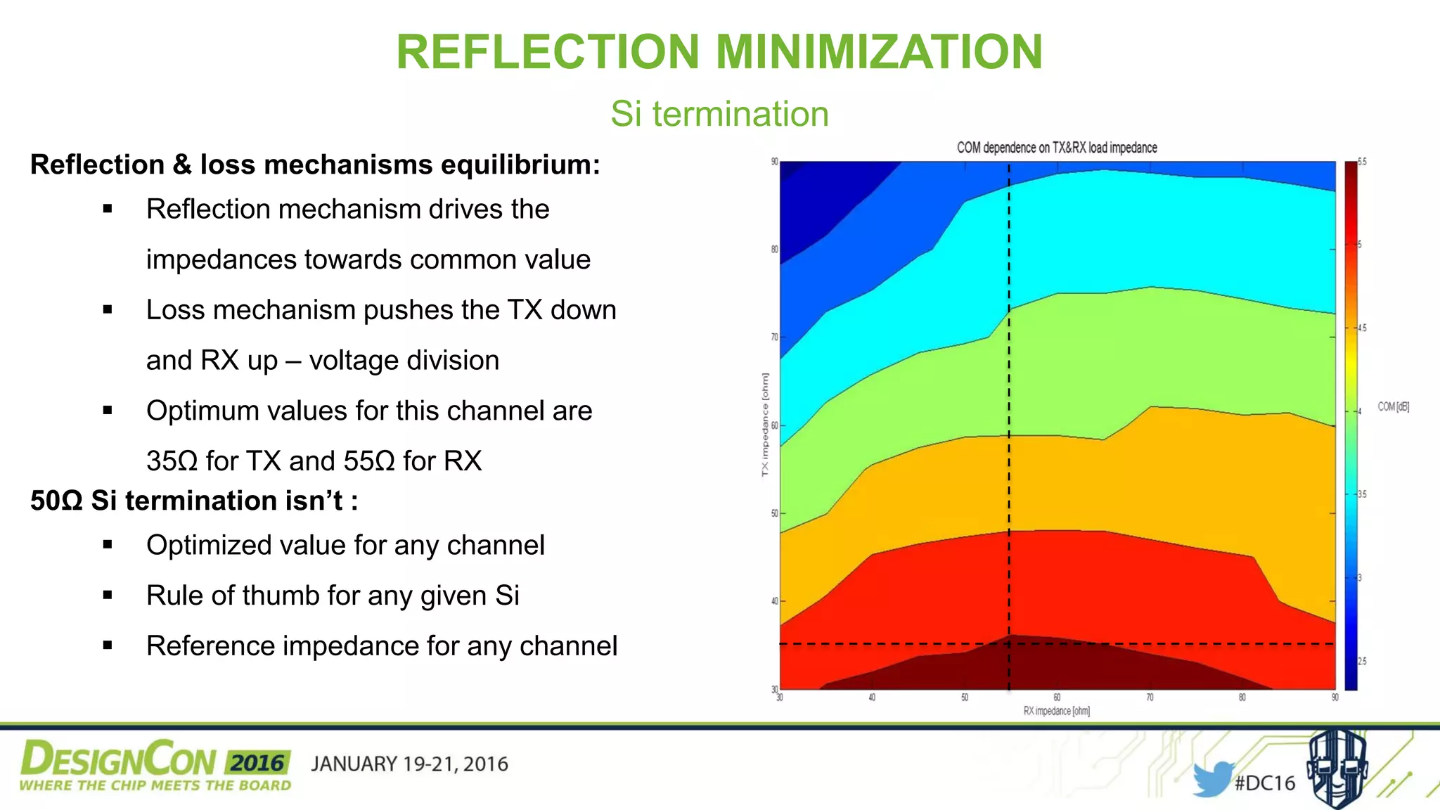
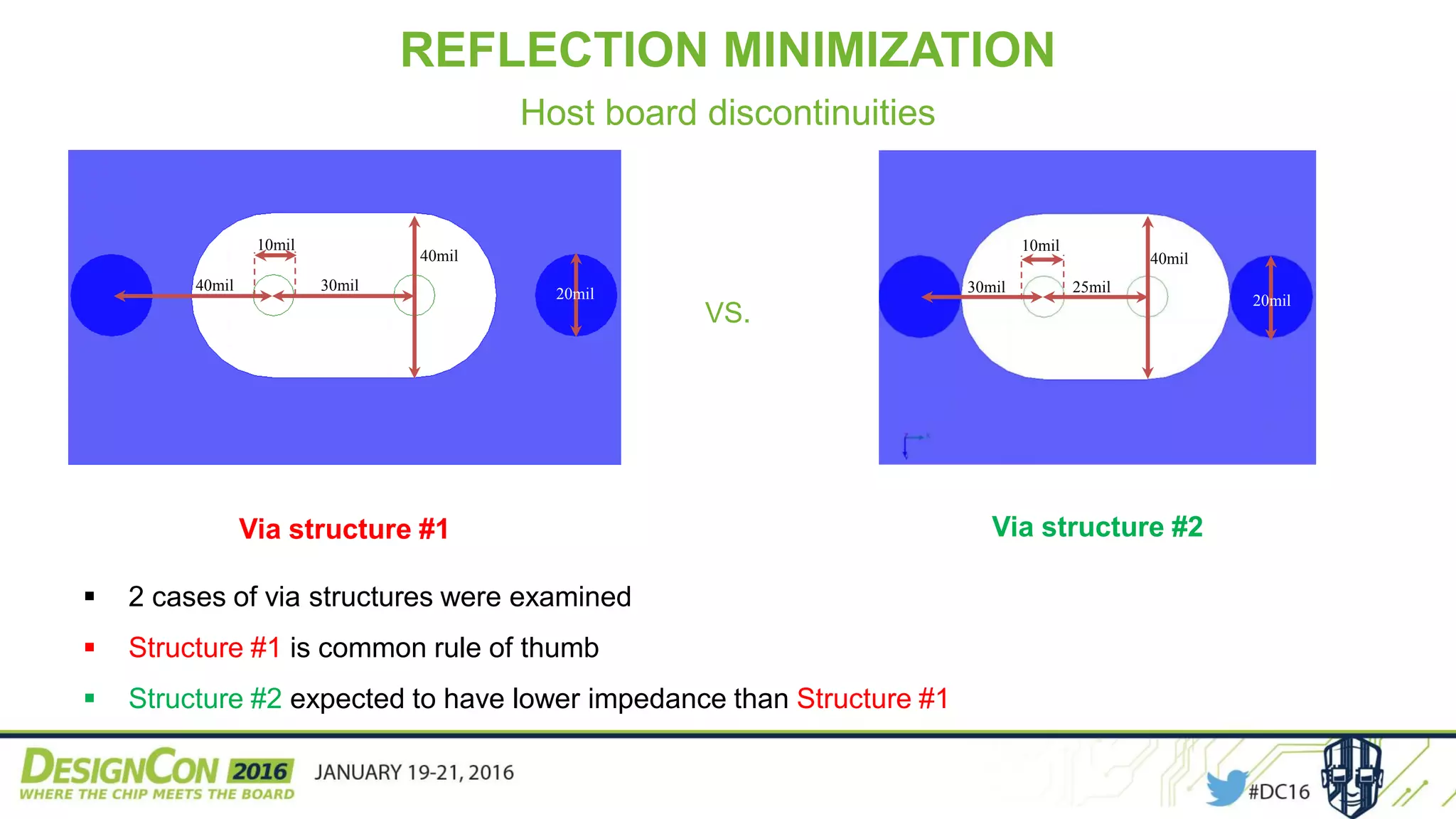
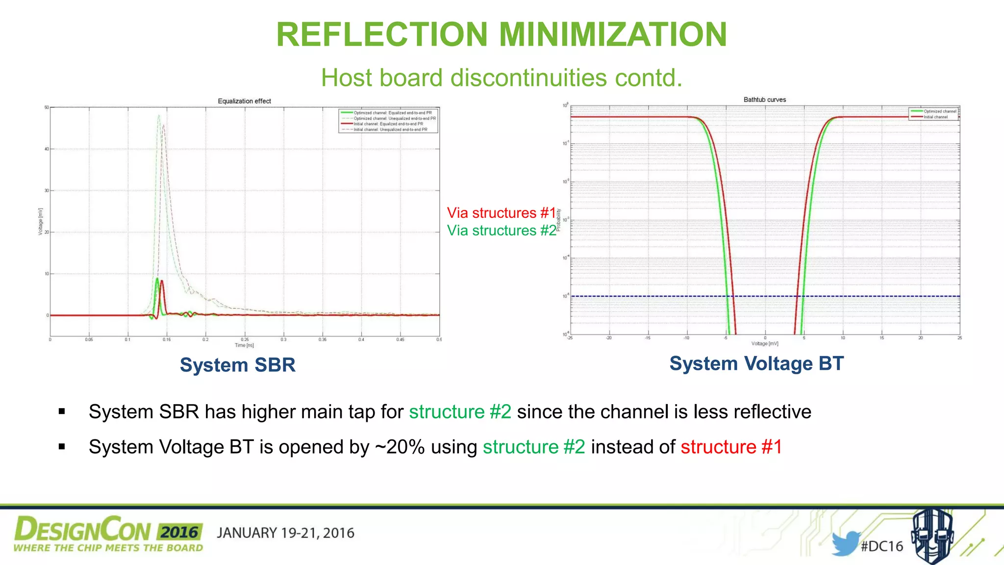
REFLECTION MINIMIZATION
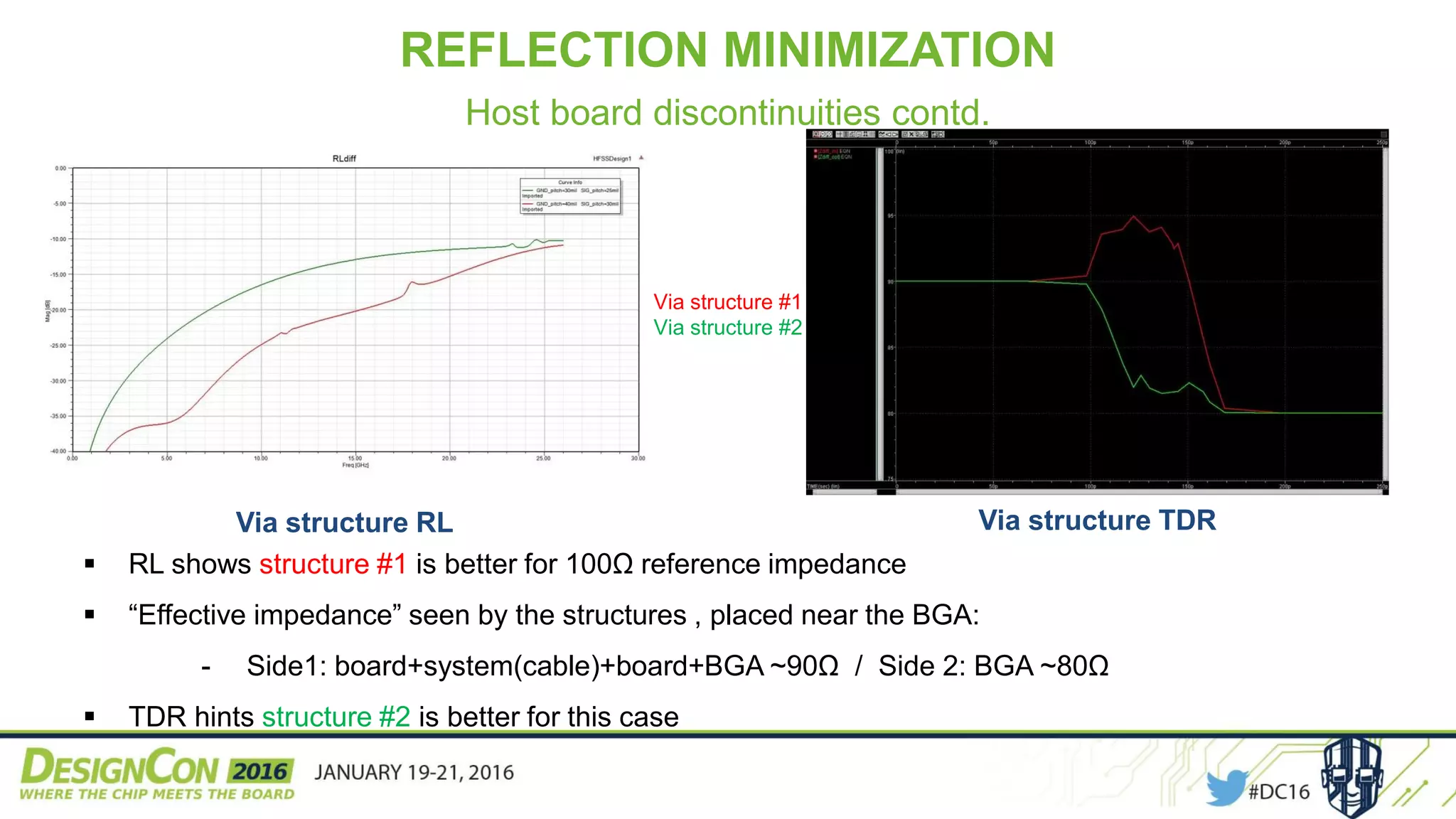
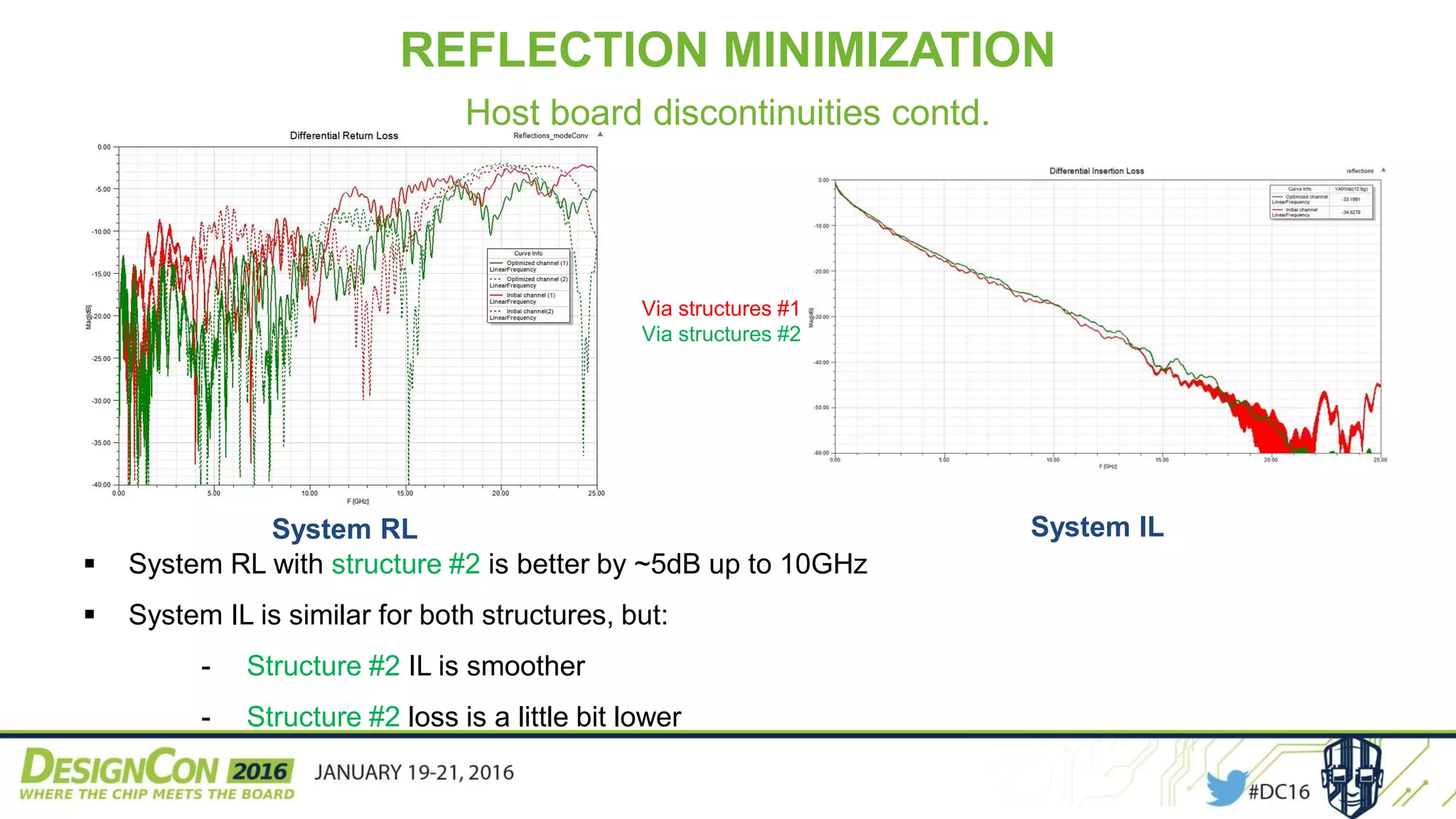
Host board discontinuities contd.
COM increased by 0.75dB meeting the pass criteria!
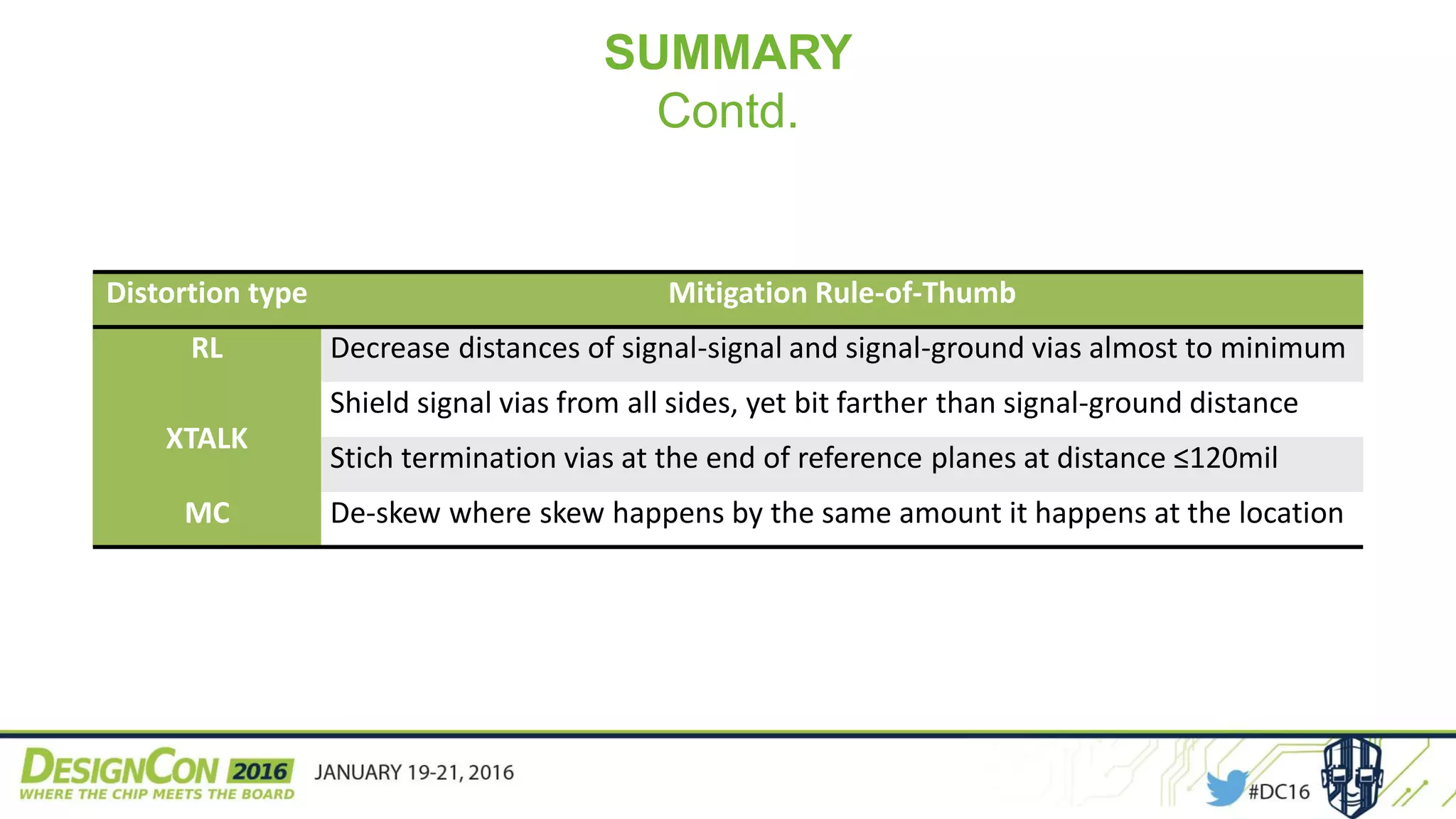
General design guidelines :
Usually the “effective impedance” of the system is lower than 100Ω
Match discontinuities impedance to the “effective impedance”
of the system by making them as transparent as possible
For this test case almost minimum distances of S-S and S-G give the best results](https://image.slidesharecdn.com/zx8bipadrewyjh2vwzvv-signature-e78e649b7064cbb66b13324d0d7565661a68eb1b3a51de5fddac0dea838a9858-poli-160123035250/75/Slides-are-thereanyrulesofthumb_brener-14-2048.jpg)
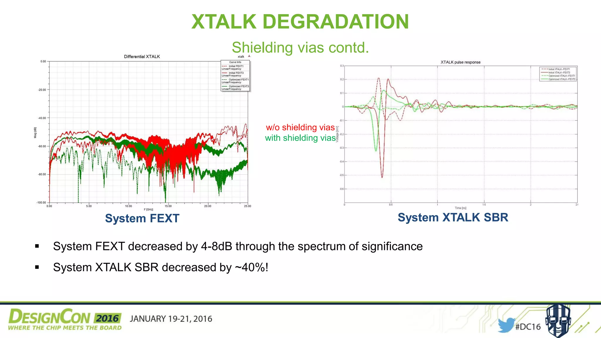
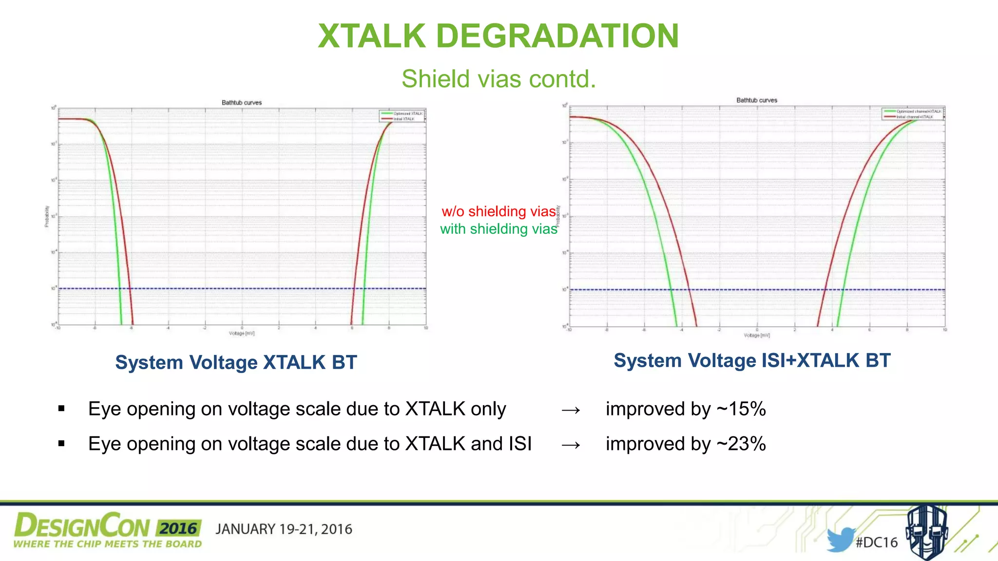
![Systems with via structures COM [dB]
w/o shielding vias 3.1
with shielding vias 3.35
COM increased by 0.25dB!
General design guidelines :
Don’t base XTALK expectations purely on the distance and symmetry of the vias
Shield signal vias from all sides, yet bit farther than S-G distance
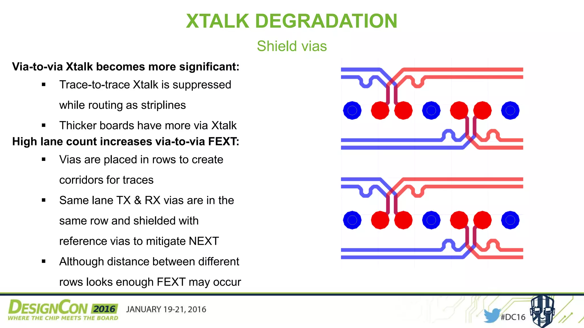
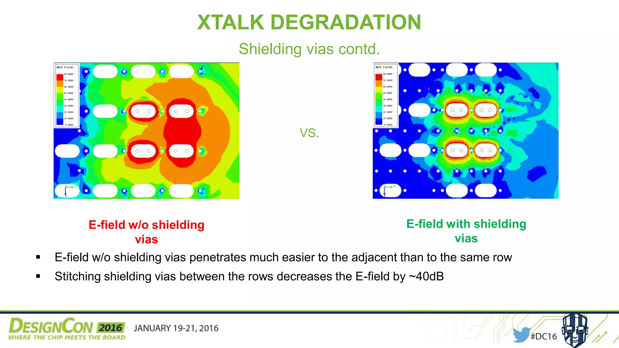
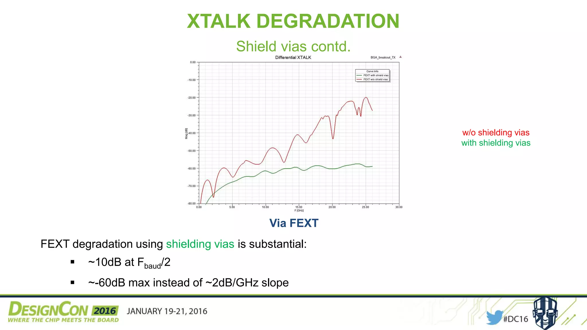
XTALK DEGRADATION
Shield vias contd.](https://image.slidesharecdn.com/zx8bipadrewyjh2vwzvv-signature-e78e649b7064cbb66b13324d0d7565661a68eb1b3a51de5fddac0dea838a9858-poli-160123035250/75/Slides-are-thereanyrulesofthumb_brener-20-2048.jpg)
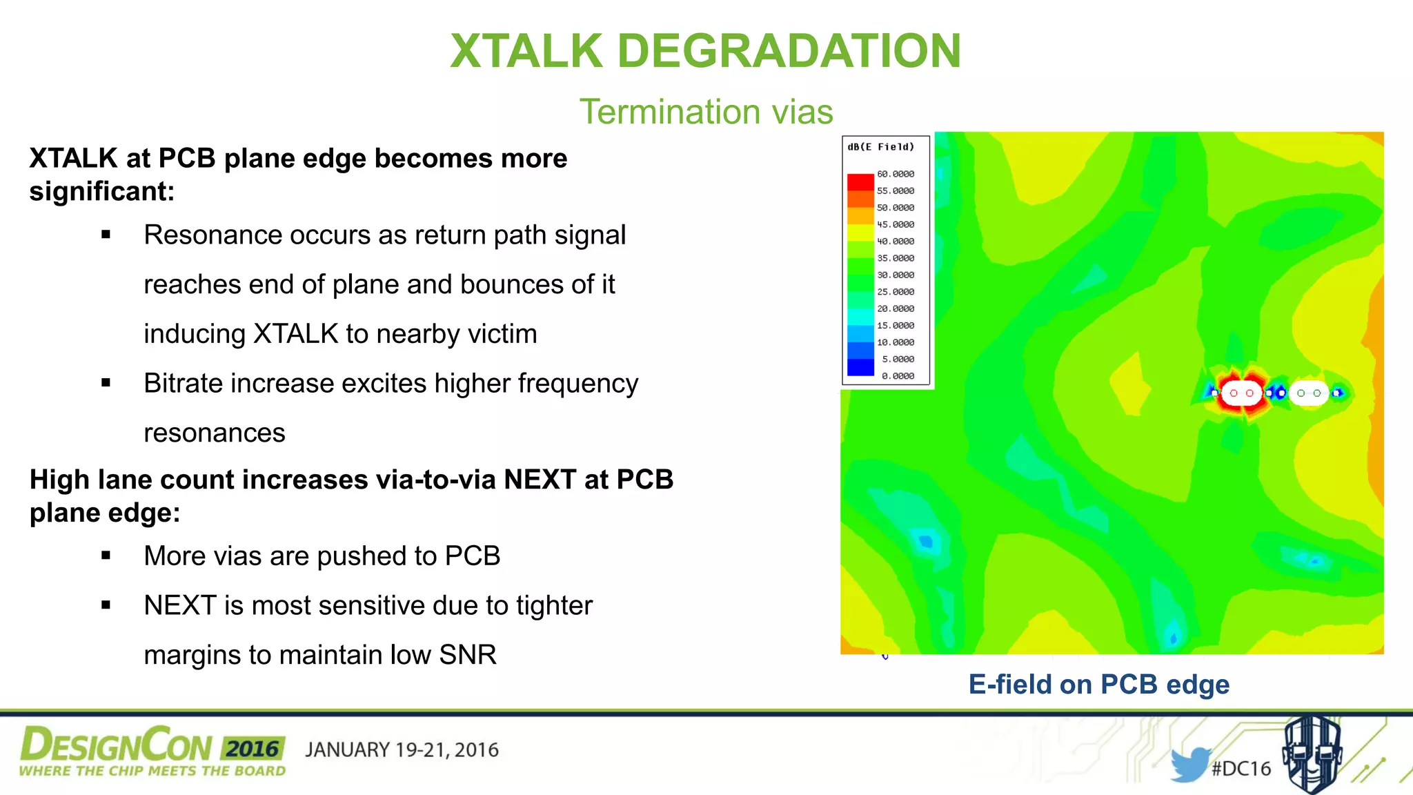
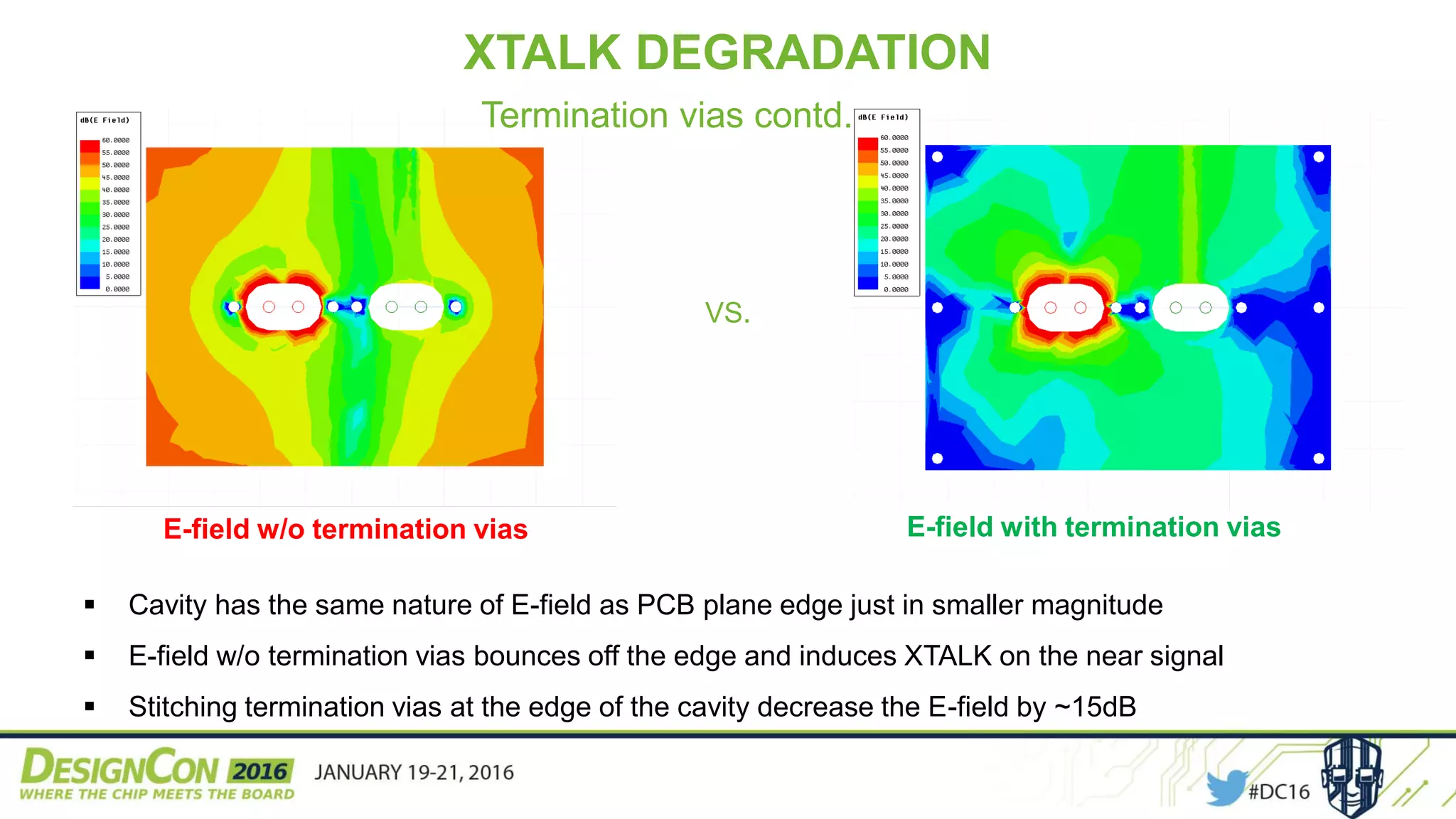
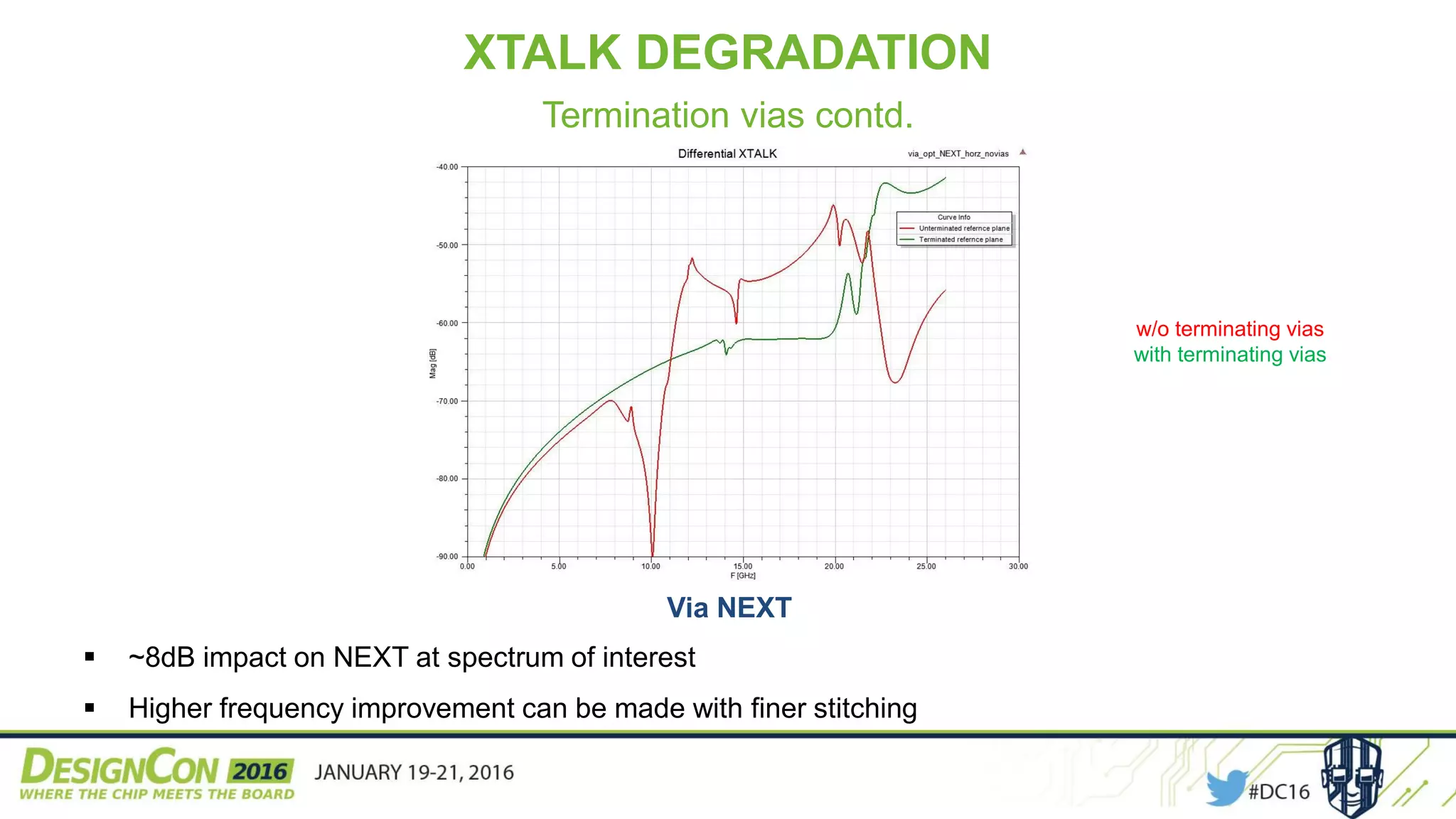
![Systems type COM [dB]
w/o terminating vias 3.15
with terminating vias 3.25
COM increased by 0.1dB w/o any real effort!
Stitch the edge of the reference plain with terminating vias
Via-to-via distance ≤120mil for 25Gbps
For other rates use: 𝑑 𝑚𝑎𝑥 =
𝑣
2𝐹 𝑏𝑎𝑢𝑑
XTALK DEGRADATION
Termination vias contd.](https://image.slidesharecdn.com/zx8bipadrewyjh2vwzvv-signature-e78e649b7064cbb66b13324d0d7565661a68eb1b3a51de5fddac0dea838a9858-poli-160123035250/75/Slides-are-thereanyrulesofthumb_brener-24-2048.jpg)
![System design phase COM [dB]
Initial 2.35 (FAIL)
Optimized 3.35 (PASS)
COM increased by 1dB , in this case equivalent to ~1in
margin in PCB trace length!
Proper via treatment can increase system’s COM by:
0.75dB – via matching to the “effective impedance”
0.25dB – reference via shielding
SUMMARY](https://image.slidesharecdn.com/zx8bipadrewyjh2vwzvv-signature-e78e649b7064cbb66b13324d0d7565661a68eb1b3a51de5fddac0dea838a9858-poli-160123035250/75/Slides-are-thereanyrulesofthumb_brener-27-2048.jpg)

This document summarizes a presentation given by Jacov Brener and Liav Ben-Artsi of Marvell Israel Ltd on rules of thumb for 100Gb/s board design. The presentation covered COM testing methodology and optimizing the physical design to improve COM margins. Some key guidelines included minimizing reflections by matching discontinuities to the effective channel impedance, shielding signal vias to reduce crosstalk, adding termination vias at the edge of planes, and deskewing signals where skew occurs to reduce ISI. Following these guidelines such as adjusting via structures and adding shield vias increased COM by up to 1dB in examples shown, providing important margin for reliable high-speed signal transmission.


![Signal Integrity - A Crash Course [R Lott]](https://cdn.slidesharecdn.com/ss_thumbnails/1cb0870c-cad3-4a68-ad41-8e9450fec5d8-170217191645-thumbnail.jpg?width=640&height=640&fit=bounds)


