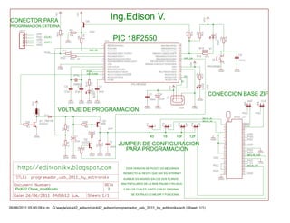
aqui les traigo el famoso pickit2 modificado no hay ningun plano en la web igual a este, este plano es producto de los demas pikit2 de los cuales me base para hacer este.
1. The document shows a circuit diagram for a high end headphone amplifier with inputs for left and right audio channels.
2. It uses operational amplifiers, transistors, resistors, and capacitors to regulate voltage and amplify the audio signal for output to headphones.
3. The amplifier can run on either 240V or 120V input and provides adjusted voltage outputs of +12V, 0V, and -12V to power the circuitry and drive the headphones.
This circuit diagram shows a USB power adapter that converts an AC input of 100-240V at 50-60Hz to a 5V 1A DC output. The main components are a transformer T1, rectifier diodes D1-D4, filter capacitors C1-C2, and voltage regulator IC1. Resistors R9-R12 and zener diode D7 form a voltage divider and reference circuit to regulate the output voltage at 5V.
This document describes the parameters for a power factor correction circuit simulation with the following key details:
1. The circuit includes components like diodes, MOSFETs, resistors, capacitors, and an IC controller.
2. Key parameters include an input AC voltage of 100V at 50Hz, inductors with values of 230uH and a ratio of 1:9.6, and a load current of 0.5A.
3. The circuit aims to provide power factor correction for an AC input voltage using the components and controller.
The document summarizes a seminar on circuit simulation and PCB design using OrCAD. It covers basics of circuits and components, concepts of printed circuit boards, the electronic system design flow, an introduction to PSPICE modeling, schematic design, PSPICE simulation, PCB design using OrCAD, and testing the design. It provides details on different types of circuits, components, printed circuit boards, the design process from schematics to simulation to PCB layout, and uses examples to illustrate transistor parameters in PSPICE models and complex schematic designs.
The document describes a Near-Field Communication (NFC) system designed by Group 31. The NFC system uses Frequency Shift Keying (FSK) to transmit data between devices over short ranges using magnetic field induction. It consists of a transmitter with a VCO modulated by a PC interface, and a receiver with an amplifier, loop antenna, and PLL for demodulation. The design achieves data rates of 800kbps over ranges of 30cm, within FCC regulations for non-radiative wireless technologies.
1. The document shows a circuit diagram for a microcontroller board using an ATmega128 microcontroller.
2. Key components include the microcontroller U3, voltage regulators VR1 and U1, oscillators Y1 and X1, and various input/output ports and connections.
3. The circuit provides power regulation and input/output interfaces to connect sensors, displays, and other peripherals to the microcontroller.
The document summarizes the specifications of a 2.4GHz wireless intercom system. It includes details on operating frequency, modulation types, battery requirements, and other technical specifications. The system uses Ni-MH rechargeable batteries and supports both FSK and DTMF modulation to enable voice and signal transmission between connected devices. It provides basic point-to-point and multi-point communication capabilities.
This document provides a circuit diagram for a high voltage power supply. The circuit uses a 240V AC input which is filtered and regulated to produce 12V DC power. A switching circuit then converts the 12V to high voltage DC power output through a transformer circuit using a neon indicator lamp and silicon diodes for protection. The high voltage DC output can be varied through an optional capacitor and is limited to approximately 300V maximum.
The document describes an 8-bit pipelined analog-to-digital converter (ADC) with a selectable resolution of 5-8 bits. The ADC was fabricated in a 0.13-micron CMOS process and achieves an effective number of bits of 6.10 in 8-bit mode with a 162 MHz input signal. Key aspects of the ADC include double sampling to relax amplifier settling times, redundant sign digit correction to compensate comparator offsets, and a two-stage op-amp design to provide sufficient gain and signal headroom given the low 1.2V supply voltage. Measured performance meets the requirements for medium resolution and sampling rate ADCs in modern synthetic aperture radar systems.
Here are the key points about where torque comes from in DC and AC motors:
DC Motor:
- Torque is directly proportional to current. Higher current results in higher torque.
- Torque can be controlled precisely by varying the current through pulse width modulation of the voltage applied to the motor.
AC Induction Motor:
- Torque is produced by the interaction between the rotating magnetic field produced by the stator windings and the magnetic field of the rotor.
- The rotating magnetic field induces currents in the rotor that produce its own magnetic field. The interaction (or induction) of the two magnetic fields causes the rotor to turn.
- Torque is highest at lower speeds when there is a larger difference between
The document provides a device modeling report for a Toshiba TA7291P bridge driver IC. It includes:
- Component and part number details
- Circuit simulations and evaluation circuits showing the IC's operation under different input and output conditions
- Simulation results analyzing key parameters like supply current, input characteristics, saturation voltages, and diode characteristics.
The report concludes with 11 sections summarizing the IC's electrical behavior and performance based on circuit simulations, with tables comparing simulated and measured values.
The LMH6321 is a high speed buffer that can drive ±300 mA continuously with an adjustable current limit between 10 mA and 300 mA. It has a high slew rate of 1800 V/μs and bandwidth of 110 MHz. The device features thermal shutdown protection and an error flag output. It is available in 8-pin PSOP and 7-pin TO-263 packages.
This document describes a mathematical approach to generating a pure sine wave using a microcontroller. It divides the sine wave into small segments to approximate the shape. The microcontroller then produces a pulse train that is fed to a MOSFET switching circuit and transformer to generate the output sine wave. Testing showed the output had 5-8% total harmonic distortion, with the second and third harmonics being the largest. Software code is included to control the system and generate the pulse-width modulation signal.
This document contains a diagram of the pin connections for an integrated circuit. It shows the pin numbers and names for various input and output pins including a reference clock, system clock, Bluetooth pins, FM radio pins, I2S/PCM pins, and other control pins. Component designators and values are also listed for external passive components connected to some of the pins.
The document summarizes an SPICE model of a 3-phase AC motor that can accurately reproduce: (1) frequency characteristics (impedance characteristics), (2) reverse electromotive force characteristics, and (3) physical characteristics. It provides details on parameter settings for the model, the simulation circuit diagram, and simulation results showing characteristics like phase current, back-EMF, speed, torque, power output, and efficiency under varying load conditions.
This document provides a device modeling report for a PWM stepping motor driver with the part number TB62206FG manufactured by Toshiba. The report details the circuit configuration including components, block diagrams of subcircuits, parameter definitions, and simulation results comparing phase input to phase output current.
The document discusses a schedule for an intensive coaching batch (ICB) with the first list of selected students to be displayed between June 18-20 and the second list to be based on tests from June to September, with details of the ICB working to
1) The experiment demonstrated pulse code modulation (PCM) encoding using an analog-to-digital converter (ADC) and decoding using a digital-to-analog converter (DAC).
2) The sampling frequency determined by the pulse generator was measured to be 250 kHz, which was higher than twice the analog input frequency, satisfying the Nyquist criterion.
3) After low-pass filtering the DAC output, the waveform was smoothed into a close approximation of the original analog input signal.
This document describes the features and specifications of the AT89S8252 microcontroller. It has 8K bytes of flash memory, 2K bytes of EEPROM, and 256 bytes of RAM. It supports SPI serial interfacing and has 32 I/O lines, three timers, interrupts, and low power modes. The flash can be reprogrammed in-system through an SPI interface or programmer to update code.
The document describes the ST16C550 UART chip, which features a 16-byte transmit FIFO, 16-byte receive FIFO, and full duplex operation. It is pin-compatible with the NS16C550 UART and operates at speeds from 2.97V to 5.5V with a programmable baud rate generator from 50 bps to 1.5 Mbps. The chip provides status registers for error conditions and transfer status as well as interrupt capabilities. It is available in 40-pin PDIP, 44-pin PLCC, and 48-pin TQFP packages.
The document summarizes a high-side power switch component. It includes a block diagram showing an N-channel MOSFET power transistor with input, enable, and output pins. It describes the characteristics of the input pin, enable pin, on-state resistance, and turn on/off timing. Simulation results are shown comparing the component's behavior to measurements for various operating conditions.
The document is a periodic table of the elements that lists all 118 known elements by their atomic number, element name, symbol, atomic mass, and classification. It provides the essential information about all elements in an organized table format for easy reference.
1. The document is the periodic table of elements, which classifies all known elements.
2. Elements are classified by their atomic number and arranged in rows and vertical columns.
3. Elements in the same column have similar chemical properties because they have the same number of electrons in their outer shell.
The buck converter simulation example evaluates the switching waveforms and power switch voltages and currents. The specifications include a voltage output of 5V from an input voltage ranging from 7-40V. Inductor and capacitor values are selected to be 330uH and 330uF respectively. Simulation results are obtained for the switching waveforms, power switch voltages and currents using the average models with analysis directives to skip the breakpoints for a 10ms transient simulation.
This document describes an experiment on pulse code modulation (PCM) using an analog-to-digital converter (ADC) and digital-to-analog converter (DAC). The objectives are to demonstrate PCM encoding and decoding, show how the ADC sampling rate relates to analog signal frequency, and examine the effect of low-pass filtering on the DAC output. The experiment involves using an 8-bit ADC to sample an analog signal and an 8-bit DAC to reconstruct the signal, with a low-pass filter to smooth the DAC output.
This document describes an experiment to demonstrate pulse-code modulation (PCM) using an analog-to-digital converter (ADC) and a digital-to-analog converter (DAC). The objectives are to encode and decode analog signals using PCM and demonstrate how the sampling rate affects the reproduction of analog signals. The experiment uses an 8-bit ADC to sample an analog input signal and convert it to an 8-bit digital code. The digital output is then converted back to an analog signal using an 8-bit DAC. A low-pass filter is used to smooth the staircase output of the DAC into a representation of the original analog input signal.
The document provides information about the 74HC/HCT4020 integrated circuit, which is a 14-stage binary ripple counter. It has 12 parallel outputs, a clock input, and an overriding asynchronous master reset input. The counter advances on the falling edge of the clock input and the master reset input asynchronously clears all counter stages and forces the outputs low. The document includes specifications, pin descriptions, logic diagrams, timing diagrams, and package information.
This document contains a schematic diagram of an LCD display module connected to a microcontroller. Key components include:
- A microcontroller labeled U1 connected to the LCD display via various pins for controlling the LCD.
- An LCD display module with connections for power (VDD, VSS, VEE), data lines (D0-D7), control lines (RS, RW, E), and a resistor network.
- Oscillator and reset components connected to the microcontroller to provide clock signals and reset functionality.
This document provides a circuit diagram for a microcontroller development board. It includes the microcontroller IC, LEDs, buttons, oscillators, and power supply components connected with resistors and capacitors. The microcontroller is an XC6202P332TB with various pins labeled for inputs, outputs, power, and debugging interfaces.
The document describes a buck converter design using a μPC494 controller. Key points:
1. The buck converter steps down 12V input to a regulated 5V, 0.5A output. Simulation results show output voltage regulation to within 1%, efficiency over 74%, and response to step loads within 250mV/250mA.
2. The design utilizes a Q2SA1680 MOSFET for switching and an XBS104V14R_P Schottky diode. Waveforms show current/voltage stresses and losses are analyzed based on device characteristics.
3. Operation is explained showing voltage control loop regulating output based on sensed voltage and PWM duty cycle control of switching transistor. Key components and their
The document provides specifications for a class D audio amplifier circuit using an IRS2092 integrated circuit. It includes 3 sentences summarizing key points:
The document outlines specifications for efficiency, total harmonic distortion (THD), frequency response, output power, voltage gain, self-oscillation frequency, dead time, turn on transient, components stress, power loss in MOSFETs, short circuit response, and simulated performance with different field effect transistors (FETs). Graphs and simulation results are provided to evaluate performance across operating conditions including efficiency around 93% and THD less than 0.015% at 1kHz and 10W into a 4 ohm load. Frequency response is specified to be within ±1dB from 20
- The simulation shows the peak current in the bridge diode D1 at startup, which reaches around 140A.
- This occurs when the power supply is first turned on before it reaches steady state operation.
- The high current is due to the initial charging of the transformer primary from the DC bus capacitor.
- Over time, the current decreases as the power supply components become energized and regulated operation begins.
This document contains code for using a Proteus simulation with a PIC microcontroller to blink an LED using different methods. It defines ports and pins as inputs and outputs, and uses pause commands to turn an LED on and off at set time intervals. It also includes code for initializing an LCD display using specific port pins and bits.
The Arduino is described as being low cost, easy to use, open source and compatible with multiple platforms. The initial labs focus on basics like blinking an LED and interfacing with the serial port. Later labs introduce communicating with GPS devices and integrating multiple devices. The document outlines various common electronic components that can be interfaced with Arduino like displays, sensors and more. It also defines some common terms used and provides instructions for setting up the Arduino software and board. Contact information is provided for further queries.
This document provides an overview of the deflection circuit operation theory for an ACER V772 CRT monitor. It includes:
1) A block diagram of the deflection circuit and its main components.
2) Details on the operation of the autosync deflection controller IC, including its pin functions.
3) Descriptions of the horizontal driver and output circuit, dynamic focus circuit, brightness and spot killer circuit, B+ driver and step-up circuit, HV shutdown circuit, and horizontal linearity circuit.
4) Truth tables and diagrams to illustrate the functions and connections between components in each circuit.
This document summarizes some key points about the Arduino hardware:
- The Arduino has 20 total I/O pins that can be used for digital or analog input/output. Pins 0-13 are digital and pins 0-5 can also be used for analog.
- Pins 0 and 1 are also used for the serial RX and TX. Pins 4 and 5 are for I2C communication. Pin 13 has an on-board LED. Pins 8, 10, 11 provide PWM output.
- When starting a new project, dedicated pins like analog inputs, serial, I2C, LED and PWM should be allocated first before using the remaining pins for general I/O. Unused functions
1) Initial condition setting can shorten simulation time and improve convergence by setting component voltages and currents at the start of simulation.
2) Simulating with the VCC startup voltage and initial conditions set on other nodes showed differences in simulation time.
3) Setting the output voltage initial condition below 19V instead of simulating the VCC startup also reduced simulation time.
4) Setting initial conditions on all nodes led to the fastest simulation time of 20.3 minutes for the full circuit simulation.
The document provides instructions to build the Purple Peaker circuit. It includes a layout diagram and parts list for the circuit, which uses switches instead of potentiometers to modify the frequency response. Off-board components are not shown on the layout. The layout and parts list are intended to build the circuit described without any external modifications.
The document shows a circuit diagram for an electronic device with components including a microcontroller, crystals, capacitors, and connections for a display, laser, and servo motor. The microcontroller is an ATtiny24 and it is connected to components for timekeeping functions like setting hours, minutes, and seconds as well as controlling the laser and servo. The circuit provides power regulation and connections for programming the microcontroller.
The document describes the design and construction of a logic pulser circuit that can override the logic state of a point being tested by generating a short pulse to drive the point to the opposite logic level. The circuit uses transistors to generate a 500 nanosecond pulse when a microswitch is pressed that can set the point under test to either a logic 1 or 0, and includes protections for safety and to prevent damage to the circuit being tested. Details are provided on the circuit design and components as well as guidelines for building the pulser on a printed circuit board with a microswitch.
This document contains circuit diagrams and specifications for four different amplifier circuits:
1) A CS amplifier with a gain of 1.310uV/20mV at 1kHz frequency.
2) A CE amplifier with an output voltage of 2.005V at 1kHz frequency.
3) An RC phase shift oscillator with an output of 526.1mV at 1kHz frequency.
4) A two stage RC coupled amplifier with a gain of 6.675V/20mV at 1kHz frequency.
This document describes a ground cleaning robot that uses a microcontroller and various sensors to navigate and clean an area. It contains a microcontroller that controls input and output functions through an LCD display. It uses ultrasonic sensors to detect obstacles and switches to control cleaning motors and navigation. The robot is powered by a 12V battery and uses optocouplers to isolate motor control circuits from the microcontroller.
1. The document provides a design kit for a high-precision linear regulator with an output voltage of 5V and output current of 3A.
2. The design kit includes schematics showing the circuit components including transistors, resistors, capacitors, and integrated circuits used in the regulator design.
3. The schematics provide details on the connections between the components and labeling for voltage and current measurements.
This document provides a design kit for a ringing choke converter (RCC) circuit with the following specifications:
- Output voltage of 12V and output current of 1A
- Uses components including transistors, diodes, resistors, capacitors, and inductors in a switching converter configuration to achieve the voltage and current outputs.
- Includes a block diagram of the circuit layout and component list for the RCC design.
This document summarizes a proposed system for changing the shopping experience by integrating online and offline shopping. The system uses a mirror that takes photos of customers and uploads them to an online store. This allows customers to see how clothing items look on themselves in the mirror before purchasing items online. The system aims to extend the real shopping experience into the online realm. It proposes using sensors, cameras, and cloud technology to link what a customer sees in the mirror to personalized online shopping profiles and social sharing features. A prototype was developed to demonstrate the concept.
This document reviews SPICE simulations performed on a TTL inverter circuit. The simulations included:
1. A DC analysis to determine the circuit's transfer characteristics, threshold voltage, noise margins, and power curve.
2. An AC analysis to find the circuit's gain, input impedance, and output impedance.
3. Additional frequency analysis to characterize the circuit's behavior at different frequencies.
4. Analysis of propagation delays and rise/fall times using a 10us digital pulse input to determine switching characteristics.
The document describes the circuit schematics used for each analysis and presents the simulation settings and results. The goal is to exercise analysis tools in the circuit simulation software SPICE.
This document contains a diagram of a circuit with several components including a sensor, LCD display, mixer, and power circuit. The diagram shows the connections between an microcontroller, motor driver, buttons, resistors, and batteries. Percentages ranging from 31% to 45% are shown connected to the mixer. The purpose and function of the overall circuit is not entirely clear from the diagram and limited accompanying text alone.
Similar to Programador usb 2011_pickit2 modificado (20)
ISO/IEC 27001, ISO/IEC 42001, and GDPR: Best Practices for Implementation and...PECB
Denis is a dynamic and results-driven Chief Information Officer (CIO) with a distinguished career spanning information systems analysis and technical project management. With a proven track record of spearheading the design and delivery of cutting-edge Information Management solutions, he has consistently elevated business operations, streamlined reporting functions, and maximized process efficiency.
Certified as an ISO/IEC 27001: Information Security Management Systems (ISMS) Lead Implementer, Data Protection Officer, and Cyber Risks Analyst, Denis brings a heightened focus on data security, privacy, and cyber resilience to every endeavor.
His expertise extends across a diverse spectrum of reporting, database, and web development applications, underpinned by an exceptional grasp of data storage and virtualization technologies. His proficiency in application testing, database administration, and data cleansing ensures seamless execution of complex projects.
What sets Denis apart is his comprehensive understanding of Business and Systems Analysis technologies, honed through involvement in all phases of the Software Development Lifecycle (SDLC). From meticulous requirements gathering to precise analysis, innovative design, rigorous development, thorough testing, and successful implementation, he has consistently delivered exceptional results.
Throughout his career, he has taken on multifaceted roles, from leading technical project management teams to owning solutions that drive operational excellence. His conscientious and proactive approach is unwavering, whether he is working independently or collaboratively within a team. His ability to connect with colleagues on a personal level underscores his commitment to fostering a harmonious and productive workplace environment.
Date: May 29, 2024
Tags: Information Security, ISO/IEC 27001, ISO/IEC 42001, Artificial Intelligence, GDPR
-------------------------------------------------------------------------------
Find out more about ISO training and certification services
Training: ISO/IEC 27001 Information Security Management System - EN | PECB
ISO/IEC 42001 Artificial Intelligence Management System - EN | PECB
General Data Protection Regulation (GDPR) - Training Courses - EN | PECB
Webinars: https://pecb.com/webinars
Article: https://pecb.com/article
-------------------------------------------------------------------------------
For more information about PECB:
Website: https://pecb.com/
LinkedIn: https://www.linkedin.com/company/pecb/
Facebook: https://www.facebook.com/PECBInternational/
Slideshare: http://www.slideshare.net/PECBCERTIFICATION
Beyond Degrees - Empowering the Workforce in the Context of Skills-First.pptxEduSkills OECD
Iván Bornacelly, Policy Analyst at the OECD Centre for Skills, OECD, presents at the webinar 'Tackling job market gaps with a skills-first approach' on 12 June 2024
Level 3 NCEA - NZ: A Nation In the Making 1872 - 1900 SML.pptHenry Hollis
The History of NZ 1870-1900.
Making of a Nation.
From the NZ Wars to Liberals,
Richard Seddon, George Grey,
Social Laboratory, New Zealand,
Confiscations, Kotahitanga, Kingitanga, Parliament, Suffrage, Repudiation, Economic Change, Agriculture, Gold Mining, Timber, Flax, Sheep, Dairying,
Leveraging Generative AI to Drive Nonprofit InnovationTechSoup
In this webinar, participants learned how to utilize Generative AI to streamline operations and elevate member engagement. Amazon Web Service experts provided a customer specific use cases and dived into low/no-code tools that are quick and easy to deploy through Amazon Web Service (AWS.)
Philippine Edukasyong Pantahanan at Pangkabuhayan (EPP) CurriculumMJDuyan
(𝐓𝐋𝐄 𝟏𝟎𝟎) (𝐋𝐞𝐬𝐬𝐨𝐧 𝟏)-𝐏𝐫𝐞𝐥𝐢𝐦𝐬
𝐃𝐢𝐬𝐜𝐮𝐬𝐬 𝐭𝐡𝐞 𝐄𝐏𝐏 𝐂𝐮𝐫𝐫𝐢𝐜𝐮𝐥𝐮𝐦 𝐢𝐧 𝐭𝐡𝐞 𝐏𝐡𝐢𝐥𝐢𝐩𝐩𝐢𝐧𝐞𝐬:
- Understand the goals and objectives of the Edukasyong Pantahanan at Pangkabuhayan (EPP) curriculum, recognizing its importance in fostering practical life skills and values among students. Students will also be able to identify the key components and subjects covered, such as agriculture, home economics, industrial arts, and information and communication technology.
𝐄𝐱𝐩𝐥𝐚𝐢𝐧 𝐭𝐡𝐞 𝐍𝐚𝐭𝐮𝐫𝐞 𝐚𝐧𝐝 𝐒𝐜𝐨𝐩𝐞 𝐨𝐟 𝐚𝐧 𝐄𝐧𝐭𝐫𝐞𝐩𝐫𝐞𝐧𝐞𝐮𝐫:
-Define entrepreneurship, distinguishing it from general business activities by emphasizing its focus on innovation, risk-taking, and value creation. Students will describe the characteristics and traits of successful entrepreneurs, including their roles and responsibilities, and discuss the broader economic and social impacts of entrepreneurial activities on both local and global scales.
How to Make a Field Mandatory in Odoo 17Celine George
In Odoo, making a field required can be done through both Python code and XML views. When you set the required attribute to True in Python code, it makes the field required across all views where it's used. Conversely, when you set the required attribute in XML views, it makes the field required only in the context of that particular view.