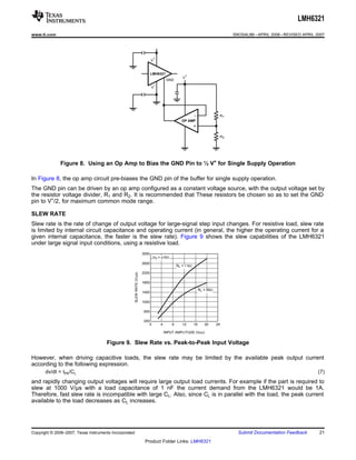
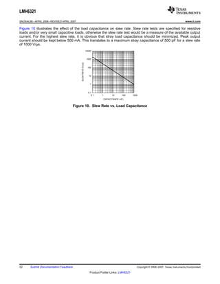
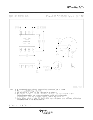
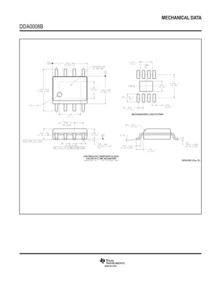
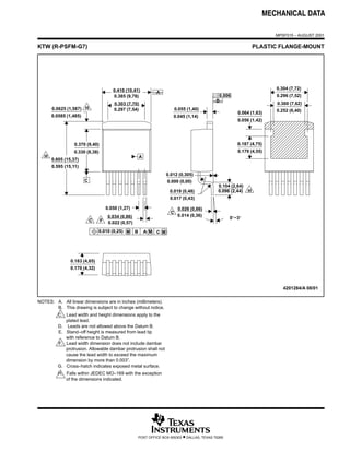
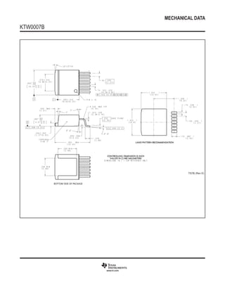
LMH6321
www.ti.com                                                                                                   SNOSAL8B – APRIL 2006 – REVISED APRIL 2007


                       LMH6321 300 mA High Speed Buffer with Adjustable Current Limit
                                                                       Check for Samples: LMH6321

1FEATURES                                                                             •   High capacitive load drive
•
2       High slew rate 1800 V/μs                                                      •   Thermal shutdown error flag
•       Wide bandwidth 110 MHz
                                                                                      APPLICATIONS
•       Continuous output current ±300 mA
•       Output current limit tolerance ±5 mA ±5%                                      •   Line driver
•       Wide supply voltage range 5V to ±15V                                          •   Pin driver
•       Wide temperature range −40°C to +125°C                                        •   Sonar driver
•       Adjustable current limit                                                      •   Motor control

DESCRIPTION
The LMH6321 is a high speed unity gain buffer that slews at 1800 V/µs and has a small signal bandwidth of 110
MHz while driving a 50Ω load. It can drive ±300 mA continuously and will not oscillate while driving large
capacitive loads.
The LMH6321 features an adjustable current limit. The current limit is continuously adjustable from 10 mA to 300
ma with a ±5 mA ±5% accuracy. The current limit is set by adjusting an external reference current with a resistor.
The current can be easily and instantly adjusted, as needed by connecting the resistor to a DAC to form the
reference current. The sourcing and sinking currents share the same current limit.
The LMH6321 is available in a space saving 8-pin PSOP or a 7-pin TO-263 power package. The PSOP package
features an exposed pad on the bottom of the package to increase its heat sinking capability. The LMH6321 can
be used within the feedback loop of an operational amplifier to boost the current output or as a stand alone
buffer.

Connection Diagram

                                                                        1                    8
                                                                 EF                              NC


                                                                        2                    7      +
                                                                 CL                              V

                                                                               G=1
                                                                        3                    6
                                                                 VIN                             VOUT


                                                                   -    4                    5
                                                                  V                              GND


                                                                        Figure 1. 8-Pin PSOP


1


             Please be aware that an important notice concerning availability, standard warranty, and use in critical applications of
             Texas Instruments semiconductor products and disclaimers thereto appears at the end of this data sheet.
2   All trademarks are the property of their respective owners.
PRODUCTION DATA information is current as of publication date.                                          Copyright © 2006–2007, Texas Instruments Incorporated
Products conform to specifications per the terms of the Texas
Instruments standard warranty. Production processing does not
necessarily include testing of all parameters.
LMH6321
SNOSAL8B – APRIL 2006 – REVISED APRIL 2007                                                                                                    www.ti.com


                                                                               G=1


                                                               1      2    3     4       5   6 7


                                                                          VOUT

                                                                                         +
                                                                          GND


                                                                                                 EF
                                                                                                 CL
                                                                VIN


                                                                                 -
                                                                                     V
                                                                                             V
         A.    V− pin is connected to tab on back of each package.

                                                         Figure 2. 7-Pin TO-263(A)

              These devices have limited built-in ESD protection. The leads should be shorted together or the device placed in conductive foam
              during storage or handling to prevent electrostatic damage to the MOS gates.


Absolute Maximum Ratings (1)
                    (2)
ESD Tolerance
      Human Body Model                                                                                                                             2.5 kV
      Machine Model                                                                                                                                 250V
Supply Voltage                                                                                                                               36V (±18V)
                                (3)
Input to Output Voltage                                                                                                                              ±5V
Input Voltage                                                                                                                                   ±VSUPPLY
                                      (4)
Output Short-Circuit to GND                                                                                                                   Continuous
Storage Temperature Range                                                                                                              −65°C to +150°C
Junction Temperature (TJMAX)                                                                                                                      +150°C
Lead Temperature
      (Soldering, 10 seconds)                                                                                                                      260°C
                                                                                                                                                       (5)
Power Dissipation
CL Pin to GND Voltage                                                                                                                              ±1.2V

(1)    Absolute Maximum Ratings indicate limits beyond which damage to the device may occur. Operating Ratings indicate conditions for
       which the device is intended to be functional, but specific performance is not guaranteed. For guaranteed specifications and the test
       conditions, see the Electrical Characteristics Table.
(2)    Human Body Model is 1.5 kΩ in series with 100 pF. Machine Model is 0Ω in series with 200 pF.
(3)    If the input-output voltage differential exceeds ±5V, internal clamping diodes will turn on. The current through these diodes should be
       limited to 5 mA max. Thus for an input voltage of ±15V and the output shorted to ground, a minimum of 2 kΩ should be placed in series
       with the input.
(4)    The maximum continuous current must be limited to 300 mA. See the Application Hints section for more details.
(5)    The maximum power dissipation is a function of TJ(MAX), θJA, and TA. The maximum allowable power dissipation at any ambient
       temperature is PD = TJ(MAX)–TA)/θJA. See Thermal Management section of the Application Hints.

Operating Ratings
Operating Temperature Range                                                                                                            −40°C to +125°C
Operating Supply Range                                                                                                                        5V to ±16V
Thermal Resistance (θJA),
                          (1)
      PSOP Package                                                                                                                              180°C/W
Thermal Resistance (θJC)
      TO-263 Package                                                                                                                               4°C/W
Thermal Resistance (θJA)
      TO-263 Package                                                                                                                             80°C/W

(1)    Soldered to PC board with copper foot print equal to DAP size. Natural convection (no air flow). Board material is FR-4.


2          Submit Documentation Feedback                                                              Copyright © 2006–2007, Texas Instruments Incorporated

                                                         Product Folder Links: LMH6321
LMH6321
www.ti.com                                                                                        SNOSAL8B – APRIL 2006 – REVISED APRIL 2007

±15V Electrical Characteristics
The following specifications apply for Supply Voltage = ±15V, VCM = 0, RL ≥ 100 kΩ and RS = 50Ω, CL open, unless otherwise
noted. Boldface limits apply for TA = TJ = TMIN to TMAX; all other limits TA = TJ = 25°C.
 Symbol                    Parameter                                  Conditions                    Min       Typ        Max       Units
AV           Voltage Gain                           RL = 1 kΩ, VIN = ±10V                          0.99       0.995
                                                                                                                                    V/V
                                                                                                   0.98
                                                    RL = 50Ω, VIN = ±10V                           0.86       0.92
                                                                                                                                    V/V
                                                                                                   0.84
VOS          Input Offset Voltage                   RL = 1 kΩ, RS = 0V                                         ±4        ±35
                                                                                                                                    mV
                                                                                                                         ±52
IB           Input Bias Current                     VIN = 0V, RL = 1 kΩ, RS = 0V                               ±2        ±15
                                                                                                                                     μA
                                                                                                                         ±17
R.IN         Input Resistance                       R.L = 50Ω                                                  250                   kΩ
CIN          Input Capacitance                                                                                 3.5                   pF
RO           Output Resistance                      IO = ±10 mA                                                 5                    Ω
IS           Power Supply Current                   RL = ∞, VIN = 0                                            11        14.5
                                                                                                                         16.5
                                                                                                                                    mA
                                                                                    750 µA into               14.9       18.5
                                                                                    CL Pin                               20.5
VO1          Positive Output Swing                  IO = 300 mA, RS = 0V, VIN = ±VS                11.2       11.9
                                                                                                   10.8
                                                                                                                                     V
             Negative Output Swing                  IO = 300 mA, RS = 0V, VIN = ±VS                           −11.3      −10.3
                                                                                                                         −9.8
VO2          Positive Output Swing                  RL = 1 kΩ, RS = 0V, VIN = ±VS                  13.1       13.4
                                                                                                   12.9
                                                                                                                                     V
             Negative Output Swing                  RL = 1 kΩ, RS = 0V, VIN = ±VS                             −13.4      −12.9
                                                                                                                         −12.6
VO3          Positive Output Swing                  RL = 50Ω, RS = 0V, VIN = ±VS                   11.6       12.2
                                                                                                   11.2
                                                                                                                                     V
             Negative Output Swing                  RL = 50Ω, RS = 0V, VIN = ±VS                              −11.9      −10.9
                                                                                                                         −10.6
VEF          Error Flag Output Voltage              RL = ∞, VIN = 0,                Normal                    5.00
                                                    EF pulled up with 5 kΩ
                                                                                    During                    0.25                   V
                                                    to +5V
                                                                                    Thermal
                                                                                    Shutdown
TSH          Thermal Shutdown Temperature           Measure Quantity is Die (Junction)                         168
                                                    Temperature                                                                      °C
                                                    Hysteresis                                                 10
ISH          Supply Current at Thermal              EF pulled up with 5 kΩ to +5V                               3                   mA
             Shutdown
PSSR         Power Supply Rejection Ratio           RL = 1 kΩ, VIN = 0V,            Positive        58         66
                                                    VS = ±5V to ±15V                                54
                                                                                                                                     dB
                                                                                    Negative        58         64
                                                                                                    54
SR           Slew Rate                              VIN = ±11V, RL = 1 kΩ                                     2900
                                                                                                                                    V/μs
                                                    VIN = ±11V, RL = 50Ω                                      1800
BW           −3 dB Bandwidth                        VIN = ±20 mVPP, RL = 50Ω                                   110                  MHz
LSBW         Large Signal Bandwidth                 VIN = 2 VPP, RL = 50Ω                                      48                   MHz
              nd
HD2          2     Harmonic Distortion              VO = 2 VPP, f = 100 kHz         RL = 50Ω                   −59
                                                                                    RL = 100Ω                  −70
                                                                                                                                    dBc
                                                    VO = 2 VPP, f = 1 MHz           RL = 50Ω                   −57
                                                                                    RL = 100Ω                  −68


Copyright © 2006–2007, Texas Instruments Incorporated                                               Submit Documentation Feedback          3
                                                         Product Folder Links: LMH6321
LMH6321
SNOSAL8B – APRIL 2006 – REVISED APRIL 2007                                                                                             www.ti.com

±15V Electrical Characteristics (continued)
The following specifications apply for Supply Voltage = ±15V, VCM = 0, RL ≥ 100 kΩ and RS = 50Ω, CL open, unless otherwise
noted. Boldface limits apply for TA = TJ = TMIN to TMAX; all other limits TA = TJ = 25°C.
    Symbol               Parameter                                    Conditions                       Min         Typ         Max        Units
HD3          3rd Harmonic Distortion               VO = 2 VPP, f = 100 kHz         RL = 50Ω                        −59
                                                                                   RL = 100Ω                       −70
                                                                                                                                           dBc
                                                   VO = 2 VPP, f = 1 MHz           RL = 50Ω                        −62
                                                                                   RL = 100Ω                       −73
en           Input Voltage Noise                   f ≥ 10 kHz                                                      2.8                    nV/
in           Input Current Noise                   f ≥ 10 kHz                                                      2.4                    pA/
ISC1         Output Short Circuit Current          VO = 0V,                        Sourcing            4.5          10         15.5
             Source (1)                            Program Current                 VIN = +3V           4.5                     15.5
                                                   into CL = 25 µA                                                                          mA
                                                                                   Sinking             4.5          10         15.5
                                                                                   VIN = −3V           4.5                     15.5
                                                   VO = 0V                         Sourcing            280         295         308
                                                   Program Current                 VIN = +3V           273                     325
                                                   into CL = 750 µA                                                                         mA
                                                                                   Sinking             280         295         310
                                                                                   VIN = −3V           275                     325
ISC2         Output Short Circuit Current          RS = 0V, VIN = +3V (1) (2)                          320         570         750
             Source                                                                                    300                     920
                                                                                                                                            mA
             Output Short Circuit Current Sink     RS = 0V, VIN = −3V (1) (2)                          300         515         750
                                                                                                       305                     910
V/I Section
CLVOS        Current Limit Input Offset Voltage    RL = 1 kΩ, GND = 0V                                             ±0.5        ±4.0
                                                                                                                                            mV
                                                                                                                               ±8.0
CLIB         Current Limit Input Bias Current      RL = 1 kΩ                                           −0.5        −0.2
                                                                                                                                            μA
                                                                                                       −0.8
CL           Current Limit Common Mode             RL = 1 kΩ, GND = −13 to +14V                         60          69
                                                                                                                                            dB
CMRR         Rejection Ratio                                                                            56

(1)   VIN = + or −4V at TJ = −40°C.
(2)   For the condition where the CL pin is left open the output current should not be continuous, but instead, should be limited to low duty
      cycle pulse mode such that the RMS output current is less than or equal to 300 mA.


4        Submit Documentation Feedback                                                         Copyright © 2006–2007, Texas Instruments Incorporated

                                                        Product Folder Links: LMH6321
LMH6321
www.ti.com                                                                                             SNOSAL8B – APRIL 2006 – REVISED APRIL 2007

±5V Electrical Characteristics
The following specifications apply for Supply Voltage = ±5V, VCM = 0, RL ≥ 100 kΩ and RS = 50Ω, CL Open, unless otherwise
noted. Boldface limits apply for TA = TJ = TMIN to TMAX; all other limits TA = TJ = 25°C.
 Symbol                  Parameter                                    Conditions                         Min        Typ       Max        Units
AV           Voltage Gain                         RL = 1 kΩ, VIN = ±3V                                   0.99      0.994
                                                                                                         0.98
                                                                                                                                         V/V
                                                  RL = 50Ω, VIN = ±3V                                    0.86       0.92
                                                                                                         0.84
VOS          Offset Voltage                       RL = 1 kΩ, RS = 0V                                                ±2.5       ±35
                                                                                                                                          mV
                                                                                                                               ±50
IB           Input Bias Current                   VIN = 0V, RL = 1 kΩ, RS = 0V                                       ±2        ±15
                                                                                                                                          μA
                                                                                                                               ±17
RIN          Input Resistance                     RL = 50Ω                                                          250                   kΩ
CIN          Input Capacitance                                                                                      3.5                   pF
RO           Output Resistance                    IOUT = ±10 mA                                                      5                    Ω
IS           Power Supply Current                 RL = ∞, VIN = 0V                                                   10       13.5        mA
                                                                                                                              14.7
                                                                                  750 μA into CL Pin                 14       17.5
                                                                                                                              19.5
VO1          Positive Output Swing                IO = 300 mA, RS = 0V, VIN = ±VS                         1.3       1.9
                                                                                                          0.9
                                                                                                                                          V
             Negative Output Swing                IO = 300 mA, RS = 0V, VIN = ±VS                                   −1.3      −0.5
                                                                                                                              −0.1
VO2          Positive Output Swing                RL = 1 kΩ, RS = 0V, VIN = ±VS                           3.2       3.5
                                                                                                                                          V
                                                                                                          2.9
             Negative Output Swing                RL = 1 kΩ, RS = 0V, VIN = ±VS                                     −3.5      −3.1
                                                                                                                                          V
                                                                                                                              −2.9
VO3          Positive Output Swing                RL = 50Ω, RS = 0V, VIN = ±VS                            2.8       3.1                   V
                                                                                                          2.5
             Negative Output Swing                RL = 50Ω, RS = 0V, VIN = ±VS                                      −3.0      −2.6
                                                                                                                                          V
                                                                                                                              −2.4
PSSR         Power Supply Rejection Ratio         RL = 1 kΩ, VIN = 0,             Positive                58         66
                                                  VS = ±5V to ±15V                                        54
                                                                                                                                          dB
                                                                                  Negative                58         64
                                                                                                          54
ISC1         Output Short Circuit Current         VO = 0V, Program Current Sourcing                       4.5        9        14.0
                                                  into CL = 25 μA          VIN = +3V                      4.5                 15.5
                                                                                  Sinking                 4.5        9        14.0
                                                                                  VIN = −3V               4.5                 15.5
                                                                                                                                          mA
                                                  VO = 0V, Program Current Sourcing                      275        290        305
                                                  into CL = 750 μA         VIN = +3V                     270                   320
                                                                                  Sinking                275        290        310
                                                                                  VIN = −3V              270                   320
ISC2         Output Short Circuit Current         RS = 0V, VIN = +3V (1) (2)                             300        470
             Source                                                                                                                       mA
                                                                        (1) (2)
             Output Short Circuit Current Sink RS = 0V, VIN = −3V                                        300        400
SR           Slew Rate                            VIN = ±2 VPP, RL = 1 kΩ                                           450
                                                                                                                                         V/μs
                                                  VIN = ±2 VPP, RL = 50Ω                                            210
BW           −3 dB Bandwidth                      VIN = ±20 mVPP, RL = 50Ω                                           90                  MHz
LSBW         Large Signal Bandwidth               VIN = 2 VPP, RL = 50Ω                                              39                  MHz
TSD          Thermal Shutdown                     Temperature                                                       170
                                                                                                                                          °C
                                                  Hysteresis                                                         10
V/I Section


(1)   For the condition where the CL pin is left open the output current should not be continuous, but instead, should be limited to low duty
      cycle pulse mode such that the RMS output current is less than or equal to 300 mA.
(2)   VIN = + or −4V at TJ = −40°C.
Copyright © 2006–2007, Texas Instruments Incorporated                                                    Submit Documentation Feedback           5
                                                          Product Folder Links: LMH6321
LMH6321
SNOSAL8B – APRIL 2006 – REVISED APRIL 2007                                                                                     www.ti.com

±5V Electrical Characteristics (continued)
The following specifications apply for Supply Voltage = ±5V, VCM = 0, RL ≥ 100 kΩ and RS = 50Ω, CL Open, unless otherwise
noted. Boldface limits apply for TA = TJ = TMIN to TMAX; all other limits TA = TJ = 25°C.
    Symbol              Parameter                                Conditions                     Min         Typ        Max         Units
CLVOS        Current Limit Input Offset         RL = 1 kΩ, GND = 0V                                         2.7         +5
                                                                                                                                    mV
             Voltage                                                                                                   ±5.0
CLIB         Current Limit Input Bias Current   RL = 1 kΩ, CL = 0V                             −0.5        −0.2
                                                                                                                                    μA
                                                                                               −0.6
CL           Current Limit Common Mode          RL = 1 kΩ, GND = −3V to +4V                     60          65
                                                                                                                                    dB
CMRR         Rejection Ratio                                                                    56


6        Submit Documentation Feedback                                                 Copyright © 2006–2007, Texas Instruments Incorporated

                                                       Product Folder Links: LMH6321
LMH6321
www.ti.com                                                                                                                                                                                                      SNOSAL8B – APRIL 2006 – REVISED APRIL 2007

                                                                                                      Typical Performance Characteristics
                                                                               Overshoot
                                                                                   vs.
                                                                             Capacitive Load                                                                                                                                  Slew Rate
                                                  60                                                                                                                                  3000
                                                                                     UNDERSHOOT
                                                                                                                                                                                      2600                                    RL = 1 k:
                                                  50

                                                                                                                                                                                      2200


                                                                                                                                                   SLEW RATE (V/Ps)
                       OVERSHOOT (%)


                                                  40
                                                                                                                                                                                      1800
                                                                            OVERSHOOT
                                                  30
                                                                                                                                                                                      1400                                                     RL = 50:
                                                  20
                                                                                                                                                                                      1000
                                                                   VIN = 100 mVPP
                                                  10                                                                                                                                   600
                                                                   RL = OPEN
                                                                   VS = ±15V
                                                       0                                                                                                                               200
                                                                                                                                                                                                          0         4          8          12          16    20
                                                              10               100               1k              10k
                                                                                                                                                                                                                        SUPPLY VOLTAGE (±V)
                                                                                     CL (pF)

                                                                                 Slew Rate                                                                                                                Small Signal Step Response
                                                  3000


                                                                                                                                                                    OUTPUT SIGNAL
                                                                   VS = ±15V
                                                  2600
                                                                                     RL = 1 k:

                                                  2200
               SLEW RATE (V/Ps)


                                                                                                                                                                                                                        VIN = 200 mVPP


                                                                                                                                                                                       (100 mV/DIV)
                                                  1800                                                                                                                                                                  RL = 1 k:
                                                                                                                                                                                                                        VS = ±5V
                                                                                                      RL = 50:


                                                                                                                                                                 INPUT SIGNAL
                                                  1400

                                                  1000

                                                   600

                                                  200
                                                     0                  4       8        12      16      20       24                                                                                                      TIME (10 ns/DIV)

                                                                            INPUT AMPLITUDE (VPP)
                                                                                                                                                                                                      Input Offset Voltage of Amplifier
                                                                                                                                                                                                                     vs.
                                                                   Small Signal Step Response                                                                                                                  Supply Voltage
                                                                                                                                                                                      10
                                  OUTPUT SIGNAL


                                                                                                                                                                                                                                       25°
                                                                                                                                                                                                                                         C
                                                                                                                                                          INPUT OFFSET VOLTAGE (mV)


                                                                                                                                                                                                              85°
                                                                                                                                                                                                                C
                                                                                                                                                                                           9
                                                                             VIN = 200 mVPP
                                                    (100 mV/DIV)


                                                                             RL = 1 k:
                                                                             VS = ±15V                                                                                                     8
                             INPUT SIGNAL


                                                                                                                                                                                                                           125°
                                                                                                                                                                                                                              C
                                                                                                                                                                                                                                               -40°
                                                                                                                                                                                                                                                  C
                                                                                                                                                                                           7


                                                                                                                                                                                          6
                                                                               TIME (10 ns/DIV)                                                                                                       3         5         7        9      11          13   15
                                                                                                                                                                                                                    SUPPLY VOLTAGE (±V)

                                                                   Small Signal Step Response                                                                                                             Small Signal Step Response
                              OUTPUT SIGNAL


                                                                                                                                                                  OUTPUT SIGNAL


                                                                             VIN = 200 mVPP                                                                                                                          VIN = 200 mVPP
                                                   (100 mV/DIV)


                                                                                                                                                                                      (100 mV/DIV)


                                                                             RL = 50:                                                                                                                                RL = 50:
                                                                             VS = ±5V                                                                                                                                VS = ±15V
                            INPUT SIGNAL


                                                                                                                                                               INPUT SIGNAL


                                                                               TIME (10 ns/DIV)                                                                                                                           TIME (10 ns/DIV)


Copyright © 2006–2007, Texas Instruments Incorporated                                                                                                                                                               Submit Documentation Feedback                      7
                                                                                                                       Product Folder Links: LMH6321
LMH6321
SNOSAL8B – APRIL 2006 – REVISED APRIL 2007                                                                                                                                                     www.ti.com

                                                           Typical Performance Characteristics (continued)
             Large Signal Step Response—Leading Edge                                                             Large Signal Step Response—Leading Edge
                                            VIN = 20 VPP                                                                                             VIN = 20 VPP
                OUTPUT SIGNAL


                                                                                                                      OUTPUT SIGNAL
                                            RL = 1 k:                                                                                                RL = 50:
                                            VS = ±15V                                                                                                VS = ±15V
                                 (5V/DIV)


                                                                                                                                         (5V/DIV)
                INPUT SIGNAL


                                                                                                                      INPUT SIGNAL
                                                        TIME (5 ns/DIV)                                                                                          TIME (5 ns/DIV)

             Large Signal Step Response — Trailing Edge                                                          Large Signal Step Response — Trailing Edge
                                                                       VIN = 20 VPP                                                                                             VIN = 20 VPP


                                                                                                                         OUTPUT SIGNAL
                OUTPUT SIGNAL


                                                                       RL = 1 k:                                                                                                RL = 50:
                                                                       VS = ±15V                                                                                                VS = ±15V


                                                                                                                                          (5V/DIV)
                                 (5V/DIV)


                                                                                                                         INPUT SIGNAL
                INPUT SIGNAL


                                                        TIME (5 ns/DIV)                                                                                          TIME (5 ns/DIV)

                                            Large Signal Step Response                                                                               Large Signal Step Response
                                      RL = 1 k:                                                                                                 RL = 50:
                                      VS = ±5V                                                                                                  VS = ±15V
               VOUT (0.5V/DIV)


                                                                                                                       VOUT (2V/DIV)


                                                    TIME (20 ns/DIV)                                                                                         TIME (20 ns/DIV)
                                            Large Signal Step Response                                                                               Large Signal Step Response
                                      RL = 50:                                                                                                  RL = 1 k:
                                      VS = ±5V                                                                                                  VS = ±15V
               VOUT (0.5V/DIV)


                                                                                                                       VOUT (2V/DIV)


                                                    TIME (20 ns/DIV)                                                                                         TIME (20 ns/DIV)


8       Submit Documentation Feedback                                                                                                           Copyright © 2006–2007, Texas Instruments Incorporated

                                                                                      Product Folder Links: LMH6321
LMH6321
www.ti.com                                                                                                                                                            SNOSAL8B – APRIL 2006 – REVISED APRIL 2007

                                                                       Typical Performance Characteristics (continued)
                                          Harmonic Distortion with 50Ω Load                                                                             Harmonic Distortion with 100Ω Load
                                         -20                                                                                                           -20
                                                   VS = ±15V                                                                                                      VS = ±15V
                                                   f = 1 MHz                                                                                                      f = 1 MHz
                                         -30                                                                                                           -30


                                                                                                                                   HD2 and HD3 (dBc)
                 HD2 and HD3 (dBc)


                                         -40                          HD2                                                                              -40


                                                                                                                                                       -50                         HD2
                                         -50


                                         -60                                                                                                           -60
                                                                      HD3
                                         -70                                                                                                           -70
                                                                                                                                                                                HD3

                                         -80                                                                                                           -80
                                               0        5        10        15         20    25   30                                                           0        5      10      15         20    25   30
                                                        OUTPUT AMPLITUDE (VPP)                                                                                         OUTPUT AMPLITUDE (VPP)

                                                                                                                                                                                 Noise
                                                                                                                                                                                  vs.
                                          Harmonic Distortion with 50Ω Load                                                                                                    Frequency
                                         -30                                                                                                     10000
                                                   VS = ±15V
                                         -35 R = 50:
                                               L
                                             f = 100 kHz                                                                                               1000
                                         -40
                                                                      HD2
                       HD2 & HD3 (dBc)


                                         -45
                                                                                                                                                       100                 VOLTAGE nV/ Hz)


                                                                                                                                   NOISE
                                         -50
                                                                                                                                                        10
                                         -55
                                                                                  HD3                                                                             CURRENT pA/ Hz)
                                         -60
                                                                                                                                                        1.0
                                         -65

                                         -70                                                                                                            0.1
                                               0        5             10         15        20    25                                                       1.0          10       100         1k        10k   100k
                                                            OUTPUT VOLTAGE (V)                                                                                                FREQUENCY (Hz)

                                                                    Gain                                                                                                          Gain
                                                                     vs.                                                                                                           vs.
                                                                 Frequency                                                                                                     Frequency
                                          5                                                                                                              5


                                          0                                                                                                              0


                                          -5                                                                                                            -5
                GAIN (dB)


                                                                                                                                  GAIN (dB)


                                         -10                                                                                                           -10


                                         -15                                                                                                           -15


                                         -20                                                                                                           -20
                                                   VS = ±5V                                                                                                       VS = ±15V
                                                   RL = 50:                                                                                                 RL = 50:
                                         -25                                                                                                           -25
                                           100k             1M             10M         100M      1G                                                      100k      1M                 10M         100M      1G
                                                               FREQUENCY (Hz)                                                                                                 FREQUENCY (Hz)


Copyright © 2006–2007, Texas Instruments Incorporated                                                                                                                      Submit Documentation Feedback                 9
                                                                                                      Product Folder Links: LMH6321
LMH6321
SNOSAL8B – APRIL 2006 – REVISED APRIL 2007                                                                                                                                                                                    www.ti.com

                                                                           Typical Performance Characteristics (continued)
                                                                            Gain                                                                                                               Gain
                                                                             vs.                                                                                                                vs.
                                                                         Frequency                                                                                                          Frequency
                                          5                                                                                                                         5


                                          0                                                                                                                         0


                                          -5                                                                                                                        -5
              GAIN (dB)


                                                                                                                                        GAIN (dB)
                                         -10                                                                                                                       -10


                                         -15                                                                                                                       -15
                                                   VS = ±15V                                                                                                                 VS = ±5V
                                                   RL = 1 k:                                                                                                           RL = 1 k:
                                         -20                                                                                                                       -20
                                           100k               1M               10M        100M             1G                                                        100k      1M                  10M     100M          1G
                                                                 FREQUENCY (Hz)                                                                                                         FREQUENCY (Hz)
                                                                 Supply Current                                                                                                      Output Impedance
                                                                      vs.                                                                                                                   vs.
                                                                 Supply Voltage                                                                                                      Sourcing Current
                                         14                                                                                                                        5.2
                                                             125°
                                                                C                                                                                                                                              VS = ±5V
                                                                                                                                                                                        -40°
                                                                                                                                                                                           C
                                         12
                                                                 85°
                                                                   C                                                                                                 5


                                                                                                                                            OUTPUT IMPEDANCE (:)
                   SUPPLY CURRENT (mA)


                                         10                                    25°
                                                                                 C
                                                                                     -40°
                                                                                        C                                                                          4.8
                                          8                                                                                                                                      125°
                                                                                                                                                                                    C

                                          6
                                                                                                                                                                   4.6

                                          4                                                                                                                                             25°
                                                                                                                                                                                          C          85°
                                                                                                                                                                                                       C
                                                                                                                                                                   4.4
                                          2

                                          0                                                                                                                        4.2
                                               1     3       5       7     9    11   13    15    17    19                                                                5      7       9     11    13   15    17   19
                                                             SUPPLY VOLTAGE (±V)                                                                                                    SOURCING CURRENT (mA)

                                                              Output Impedance                                                                                                       Output Impedance
                                                                     vs.                                                                                                                    vs.
                                                               Sinking Current                                                                                                       Sourcing Current
                                         5.6                                                                                                                         5
                                                   VS = ±5V                                                                                                                                                   VS = ±15V
                                                                           -40°
                                                                              C
                                         5.4                                                                                                                       4.8
                OUTPUT IMPEDANCE (:)


                                                                                                                                          OUTPUT IMPEDANCE (:)


                                                                                                                                                                                            -40°
                                                                                                                                                                                               C

                                         5.2                                                                                                                       4.6


                                                                                 125°
                                                                                    C                                                                                                                25°
                                                                                                                                                                                                       C
                                           5                                                                                                                       4.4


                                         4.8                                                                                                                       4.2
                                                                                          85°
                                                                                            C                                                                                           125°
                                                                                                                                                                                           C               85°
                                                                                                                                                                                                             C
                                                                           25°
                                                                             C
                                         4.6                                                                                                                         4
                                               5         7       9        11    13    15    17        19                                                                 5      7       9     11    13   15    17   19
                                                             SINKING CURRENT (mA)                                                                                                   SOURCING CURRENT (mA)


10      Submit Documentation Feedback                                                                                                                                Copyright © 2006–2007, Texas Instruments Incorporated

                                                                                                            Product Folder Links: LMH6321
LMH6321
www.ti.com                                                                                                                                                            SNOSAL8B – APRIL 2006 – REVISED APRIL 2007

                                                                      Typical Performance Characteristics (continued)
                                                           Output Impedance
                                                                  vs.                                                           Output Short Circuit Current—Sourcing vs.
                                                            Sinking Current                                                                 Program Current
                                          5.2                                                                                                          400
                                                                                        VS = ±15V                                                                  VS = ±15V

                                           5
                   OUTPUT IMPEDANCE (:)


                                                                                                                                 OUTPUT CURRENT (mA)
                                                                   -40°
                                                                      C                                                                                300
                                                                                                                                                                                           125°
                                                                                                                                                                                              C

                                          4.8
                                                                                                                                                                                   85°
                                                                                                                                                                                     C            -40°
                                                                                                                                                                                                     C
                                                                                                                                                       200
                                                                             25°
                                                                               C                                                                                                           25°
                                                                                                                                                                                             C
                                          4.6

                                                                                                                                                       100
                                          4.4
                                                                                   85°
                                                                                     C
                                                               125°
                                                                  C
                                          4.2                                                                                                                0
                                                5      7       9     11     13    15     17   19                                                              25    125 225 325 425 525 625 725 825

                                                           SINKING CURRENT (mA)                                                                                          PROGRAM CURRENT (PA)

                       Output Short Circuit Current—Sinking vs.                                                                 Output Short Circuit Current—Sourcing vs.
                                  Program Current                                                                                           Program Current
                                          400                                                                                                          400
                                                                                                                                                                 VS = ±5V
                                                     VS = ±15V
                OUTPUT CURRENT (mA)


                                                                                                                                 OUTPUT CURRENT (mA)
                                          300                                                                                                          300
                                                                                 125°
                                                                                    C                                                                                                     125°
                                                                                                                                                                                             C

                                                                                         -40°
                                                                                            C                                                                                                      -40°
                                                                                                                                                                                                      C
                                          200                        85°
                                                                       C                                                                               200                         85°
                                                                                                                                                                                     C

                                                                                 25°
                                                                                   C                                                                                                       25°
                                                                                                                                                                                             C

                                          100                                                                                                          100


                                            0                                                                                                            0
                                             25       125 225 325 425 525 625 725 825                                                                     25        125 225 325 425 525 625 725 825
                                                           PROGRAM CURRENT (PA)                                                                                          PROGRAM CURRENT (PA)

                                                                                                                                                                      Positive Output Swing
                       Output Short Circuit Current—Sinking vs.                                                                                                                 vs.
                                  Program Current                                                                                                                       Sourcing Current
                                          400                                                                                                           4
                                                    VS = ±5V                                                                                                               125°
                                                                                                                                                                              C
                                                                                                                                                       3.5
                                                                                                                                                                                  85°
                                                                                                                                                                                    C
                OUTPUT CURRENT (mA)


                                          300                                                                                                           3
                                                                                                                                OUTPUT SWING (V)


                                                                                 125°
                                                                                    C
                                                                                                                                                       2.5
                                                                                                                                                                   25°
                                                                                                                                                                     C
                                                                                          -40°
                                                                                             C
                                          200                         85°
                                                                        C                                                                               2
                                                                                                                                                                           -40°
                                                                                                                                                                              C
                                                                                 25°
                                                                                   C                                                                   1.5

                                          100                                                                                                           1
                                                                                                                                                                 VS = ±5V
                                                                                                                                                                         +
                                                                                                                                                       0.5       VIN = V
                                                                                                                                                                 CL = OPEN
                                            0                                                                                                           0
                                             25       125 225 325 425 525 625 725 825
                                                                                                                                                             0        100         200    300     400      500
                                                           PROGRAM CURRENT (PA)
                                                                                                                                                                         SOURCING CURRENT (mA)


Copyright © 2006–2007, Texas Instruments Incorporated                                                                                                                      Submit Documentation Feedback             11
                                                                                                    Product Folder Links: LMH6321
LMH6321
SNOSAL8B – APRIL 2006 – REVISED APRIL 2007                                                                                                                                                                                      www.ti.com

                                                                      Typical Performance Characteristics (continued)
                                                   Negative Output Swing                                                                                                    Positive Output Swing
                                                            vs.                                                                                                                       vs.
                                                      Sinking Current                                                                                                         Sourcing Current
                                       0                                                                                                                     14
                                                                                                                                                                                 125°
                                                                                                                                                                                    C                      VS = ±15V
                                     -0.5                                                                                                                                                                            +
                                                                                                                                                                                        85°
                                                                                                                                                                                          C                VIN = V
                                                                                                                                                             13                                            CL = OPEN
                                      -1
              OUTPUT SWING (V)


                                                                                                                                         OUTPUT SWING (V)
                                                                                                                                                                      25°
                                                                                                                                                                        C
                                     -1.5                                                                                                                    12
                                                                                    -40°
                                                                                       C
                                                                                                                                                                                 -40°
                                                                                                                                                                                    C
                                      -2
                                                                                              25°
                                                                                                C
                                     -2.5                                                                                                                    11

                                      -3
                                                VS = ±5V                     85°
                                                                               C                                                                             10
                                                       -
                                     -3.5       VIN = V
                                                                                125°
                                                                                   C
                                                CL = OPEN
                                      -4                                                                                                                      9
                                                                                                                                                                  0         100         200        300      400           500
                                        -500        -400         -300        -200      -100         0
                                                                                                                                                                             SOURCING CURRENT (mA)
                                                          SINKING CURRENT (mA)
                                                   Negative Output Swing
                                                            vs.                                                                     Output Short Circuit Current—Sourcing vs.
                                                      Sinking Current                                                                            Supply Voltage
                                       -9                                                                                                                   1000
                                                                                     VS = ±15V                                                                                                                  -40°
                                                                                                                                                                                                                   C
                                                                                               -                                                                                                25°
                                                                                                                                                                                                  C
                                                                                     VIN = V
                                      -10                                                                                                                    800


                                                                                                                                    OUTPUT CURRENT (mA)
                                                                                     CL = OPEN
                OUTPUT SWING (V)


                                      -11                                                                                                                    600
                                                                              25°
                                                                                C
                                                                                           -40°
                                                                                              C                                                                                                 85°
                                                                                                                                                                                                  C
                                      -12                                                                                                                    400
                                                                                                                                                                                                                125°
                                                                                                                                                                                                                   C


                                      -13                                                                                                                    200
                                                                      125°
                                                                         C                                                                                                                                 VIN = +3
                                                                                85°
                                                                                  C                                                                                                                        CL = OPEN
                                      -14                                                                                                                        0
                                        -500        -400         -300        -200     -100          0                                                                2   4        6     8     10     12     14       16    18
                                                       SINKING CURRENT (mA)                                                                                                      SUPPLY VOLTAGE (±V)
                                                                                                                                                                            Positive Output Swing
                      Output Short Circuit Current—Sinking vs.                                                                                                                        vs.
                                  Supply Voltage                                                                                                                               Supply Voltage
                                      800                                                                                                                   15
                                                                               -40°
                                                                                  C                                                                                   RL = 50:
                                                                  25°
                                                                    C
                                                                                                                                                            13
               OUTPUT CURRENT (mA)


                                      600
                                                                                                                                        OUTPUT SWING (V)


                                                                                                                                                            11
                                                                                    85°
                                                                                      C    125°
                                                                                              C
                                                                                                                                                                                            125°
                                                                                                                                                                                               C
                                      400                                                                                                                    9

                                                                                                                                                                                 85°
                                                                                                                                                                                   C                     -40°
                                                                                                                                                                                                            C
                                                               -40°
                                                                  C                                                                                          7
                                      200                                                                                                                                                     25°
                                                                                                                                                                                                C
                                                                                    VIN = -3V                                                                5
                                                                                    CL = OPEN
                                        0                                                                                                                    3
                                            2      4       6     8      10     12     14     16     18                                                            5          7          9           11          13        15
                                                           SUPPLY VOLTAGE (±V)                                                                                                   SUPPLY VOLTAGE (±V)


12      Submit Documentation Feedback                                                                                                                            Copyright © 2006–2007, Texas Instruments Incorporated

                                                                                                        Product Folder Links: LMH6321
LMH6321
www.ti.com                                                                                                                                                                                  SNOSAL8B – APRIL 2006 – REVISED APRIL 2007

                                                                                Typical Performance Characteristics (continued)
                                                         Positive Output Swing                                                                                                              Negative Output Swing
                                                                   vs.                                                                                                                               vs.
                                                            Supply Voltage                                                                                                                     Supply Voltage
                                           15                                                                                                                                 -3
                                                     RL = 1 k:                                                                                                                                                                   RL = 50:

                                           13                                                                                                                                 -5
                                                                                                                                                                                                               -40°
                                                                                                                                                                                                                  C
                        OUTPUT SWING (V)


                                                                                                                                                   OUTPUT SWING (V)
                                           11                                                                                                                                 -7
                                                                                125°
                                                                                   C                                                                                                                                       25°
                                                                                                                                                                                                                             C
                                                                                                                                                                                                    85°
                                                                                                                                                                                                      C
                                            9                                                                                                                                 -9
                                                                 85°
                                                                   C                    -40°
                                                                                           C                                                                                                                   125°
                                                                                                                                                                                                                  C
                                            7                                                                                                                                -11
                                                                                 25°
                                                                                   C

                                            5                                                                                                                                -13


                                            3                                                                                                                                -15
                                                 5           7              9          11         13       15                                                                      5            7          9          11         13     15
                                                                 SUPPLY VOLTAGE (±V)                                                                                                                SUPPLY VOLTAGE (±V)
                                                         Negative Output Swing                                                                                                     Input Offset Voltage of Amplifier
                                                                  vs.                                                                                                                             vs.
                                                            Supply Voltage                                                                                                             Common Mode Voltage
                                            -3                                                                                                                               15
                                                                                                 RL = 1 k:                                                                              VS = ±5V


                                                                                                                                               INPUT OFFSET VOLTAGE (mV)
                                            -5
                                                                                                                                                                             10
                        OUTPUT SWING (V)


                                                                                -40°
                                                                                   C
                                            -7                                                                                                                                               -40°
                                                                                                                                                                                                C

                                                                 85°
                                                                   C                        25°
                                                                                              C
                                            -9                                                                                                                                5
                                                                                                                                                                                             25°
                                                                                                                                                                                               C
                                                                            125°
                                                                               C
                                           -11
                                                                                                                                                                              0
                                           -13                                                                                                                                                         125°
                                                                                                                                                                                                          C
                                                                                                                                                                                             85°
                                                                                                                                                                                               C
                                           -15                                                                                                                               -5
                                                 5           7              9          11         13       15                                                                      -3      -2         -1         0         1      2         3
                                                                 SUPPLY VOLTAGE (±V)                                                                                                       COMMON MODE VOLTAGE (V)

                                                                                                                                                                                    Input Bias Current of Amplifier
                                            Input Offset Voltage of Amplifier vs.                                                                                                                vs.
                                                  Common Mode Voltage                                                                                                                       Supply Voltage
                                            25                                                                                                                                0
                                                     VS = ±15V                                  125°
                                                                                                   C
                INPUT OFFSET VOLTGE (mV)


                                                                                                                                                                                             125°
                                                                                                                                                                                                C
                                                                                                                                                   INPUT BIAS CURRENT (PA)


                                            15                                                                                                                                -2
                                                                                                                                                                                                                     85°
                                                                                                                                                                                                                       C

                                                                                                       -40°
                                                                                                          C
                                             5                                                                                                                                -4
                                                     -40°
                                                        C                                       25°
                                                                                                  C
                                                                                                                                                                                                           25°
                                                                                                                                                                                                             C
                                            -5                                                                                                                                -6                                               -40°
                                                                                                                                                                                                                                  C


                                                                 85°
                                                                   C
                                           -15                                                                                                                                -8
                                                     125°
                                                        C

                                           -25                                                                                                                               -10
                                                 -12        -8         -4         0         4          8      12                                                                   3        5          7         9         11     13        15
                                                         COMMON MODE VOLTAGE (V)                                                                                                                    SUPPLY VOLTAGE (±V)


Copyright © 2006–2007, Texas Instruments Incorporated                                                                                                                                               Submit Documentation Feedback                     13
                                                                                                                   Product Folder Links: LMH6321
LMH6321
SNOSAL8B – APRIL 2006 – REVISED APRIL 2007                                                                                                                                                                                  www.ti.com

                                                                    Typical Performance Characteristics (continued)
                                          Input Offset Voltage of V/I Section vs.                                                                                   Input Offset Voltage of V/I Section vs.
                                                 Common Mode Voltage                                                                                                       Common Mode Voltage
                                            5                                                                                                                            4
                                                  VS = ±5V                                                                                                                       VS = ±15V
              INPUT OFFSET VOLTAGE (mV)


                                                                                                                                        INPUT OFFSET VOLTAGE (mV)
                                            4                                                                                                                            2
                                                                                                                                                                                                   25°
                                                                                                                                                                                                     C
                                                                             25°
                                                                               C                                                                                                      -40°
                                                                                                                                                                                         C
                                                       -40°
                                                          C
                                            3                                                                                                                            0

                                            2                                                                                                                        -2

                                                                                       -40°
                                                                                          C                                                                                                                 125°
                                                                                                                                                                                                               C
                                            1                                                                                                                        -4
                                                                   85°
                                                                     C                                                                                                                            85°
                                                                                                                                                                                                    C
                                            0                                                                                                                        -6

                                           -1                                                                                                                        -8

                                           -2                                                                                                                       -10
                                             -3      -2       -1         0         1          2     3                                                                  -12          -8       -4         0     4    8   12
                                                     COMMON MODE VOLTAGE (V)                                                                                                        COMMON MODE VOLTAGE (V)


Application Hints
BUFFERS
Buffers are often called voltage followers because they have largely unity voltage gain, thus the name has
generally come to mean a device that supplies current gain but no voltage gain. Buffers serve in applications
requiring isolation of source and load, i.e., high input impedance, low output impedance (high output current
drive). In addition, they offer gain flatness and wide bandwidth.
Most operational amplifiers, that meet the other given requirements in a particular application, can be configured
as buffers, though they are generally more complex and are, by and large, not optimized for unity gain operation.
The commercial buffer is a cost effective substitute for an op amp. Buffers serve several useful functions, either
in tandem with op amps or in standalone applications. As mentioned, their primary function is to isolate a high
impedance source from a low impedance load, since a high Z source can’t supply the needed current to the load.
For example, in the case where the signal source to an analog to digital converter is a sensor, it is recommended
that the sensor be isolated from the A/D converter. The use of a buffer ensures a low output impedance and
delivery of a stable output to the converter. In A/D converter applications buffers need to drive varying and
complex reactive loads.
Buffers come in two flavors: Open Loop and Closed Loop. While sacrificing the precision of some DC
characteristics, and generally displaying poorer gain linearity, open loop buffers offer lower cost and increased
bandwidth, along with less phase shift and propagation delay than do closed loop buffers. The LMH6321 is of the
open loop variety.
Figure 3 shows a simplified diagram of the LMH6321 topology, revealing the open loop complementary follower
design approach. Figure 4 shows the LMH6321 in a typical application, in this case, a 50Ω coaxial cable driver.
                                                                                                                                                                             +
                                                                                                                                                                         V


                                                                                                        Q5
                                                                                                                            Q7
                                                                                                                                                          Q3

                                                                                                              R1                                                    R3
                                                                                                                   D1 D3 D5 D7 D9 D11                               2:
                                                                                                             Q1

                                                                                        VIN                        D2 D4 D6 D8D10 D12                                    VOUT

                                                                                                             Q2                                                     R4
                                                                                                                                                                    2:
                                                                                                              R2

                                                                                                                                                                    Q4
                                                                                                                                 Q8
                                                                                                        Q6

                                                                                                                                                                             -
                                                                                                                                                                         V


                                                                                                  Figure 3. Simplified Schematic

14      Submit Documentation Feedback                                                                                                                                    Copyright © 2006–2007, Texas Instruments Incorporated

                                                                                                        Product Folder Links: LMH6321
LMH6321
www.ti.com                                                                                                            SNOSAL8B – APRIL 2006 – REVISED APRIL 2007

SUPPLY BYPASSING
The method of supply bypassing is not critical for frequency stability of the buffer, and, for light loads, capacitor
values in the neighborhood of 1 nF to 10 nF are adequate. However, under fast slewing and large loads, large
transient currents are demanded of the power supplies, and when combined with any significant wiring
inductance, these currents can produce voltage transients. For example, the LMH6321 can slew typically at 1000
V/μs. Therefore, under a 50Ω load condition the load can demand current at a rate, di/dt, of 20 A/μs. This current
flowing in an inductance of 50 nH (approximately 1.5” of 22 gage wire) will produce a 1V transient. Thus, it is
recommended that solid tantalum capacitors of 5 μF to 10 μF, in parallel with a ceramic 0.1 μF capacitor be
added as close as possible to the device supply pins.
                                                                                               TP1
                                                                               +
                                                              C2           V                   EF           VCL
                                                            0.1 PF
                                                                                                    R3
                                                                                        R2       10 k: 1%
                                                                           +
                                                                                        10 k: 1%
                                                                       V
                                                    R1                             EF                  50: COAXIAL
                                                   10 k:         VIN          CL                          CABLE
                                                                                 VOUT


                                                                                                                  |
                                   INPUT                               LMH6321                                               OUTPUT
                                                                                         GND          R4
                                                           CIN                                                        R6
                                                                                   -                 50:
                                                                               V                                      50:
                                                     C1
                                                    1 nF

                                                              C3
                                                            0.1 PF
                                                                               -
                                                                           V


                                    Figure 4. 50Ω Coaxial Cable Driver with Dual Supplies

For values of capacitors in the 10 μF to 100 μF range, ceramics are usually larger and more costly than
tantalums but give superior AC performance for bypassing high frequency noise because of their very low ESR
(typically less than 10 MΩ) and low ESL.

LOAD IMPEDANCE
The LMH6321 is stable under any capacitive load when driven by a 50Ω source. As shown by the Overshoot vs.
Capacitive Load graph in the Typical Performance Characteristics, worst case overshoot is for a purely
capacitive load of about 1 nF. Shunting the load capacitance with a resistor will reduce the overshoot.

SOURCE INDUCTANCE
Like any high frequency buffer, the LMH6321 can oscillate with high values of source inductance. The worst case
condition occurs with no input resistor, and a purely capacitive load of 50 pF, where up to 100 nH of source
inductance can be tolerated. With a 50Ω load, this goes up to 200 nH. However, a 100Ω resistor placed in series
with the buffer input will ensure stability with a source inductances up to 400 nH with any load.

OVERVOLTAGE PROTECTION
(Refer to the simplified schematic in Figure 3).
If the input-to-output differential voltage were allowed to exceed the Absolute Maximum Rating of 5V, an internal
diode clamp would turn on and divert the current around the compound emitter followers of Q1/Q3 (D1 – D11 for
positive input), or around Q2/Q4 (D2 – D12 for negative inputs). Without this clamp, the input transistors Q1 – Q4
would zener, thereby damaging the buffer.
To limit the current through this clamp, a series resistor should be added to the buffer input (see R1 in Figure 4).
Although the allowed current in the clamp can be as high as 5 mA, which would suggest a 2 kΩ resistor from a
15V source, it is recommended that the current be limited to about 1 mA, hence the 10 kΩ shown.


Copyright © 2006–2007, Texas Instruments Incorporated                                                                       Submit Documentation Feedback    15
                                                           Product Folder Links: LMH6321
LMH6321
SNOSAL8B – APRIL 2006 – REVISED APRIL 2007                                                                           www.ti.com

The reason for this larger resistor is explained in the following: One way that the input/output voltage differential
can exceed the Abs Max value is under a short circuit condition to ground while driving the input with up to ±15V.
However, in the LMH6321 the maximum output current is set by the programmable Current Limit pin (CL). The
value set by this pin is guaranteed to be accurate to 5 mA ±5%. If the input/output differential exceeds 5V while
the output is trying to supply the maximum set current to a shorted condition or to a very low resistance load, a
portion of that current will flow through the clamp diodes, thus creating an error in the total load current. If the
input resistor is too low, the error current can exceed the 5 mA ±5% budget.

BANDWIDTH AND STABILITY
As can be seen in the schematic of Figure 4, a small capacitor is inserted in parallel with the series input
resistors. The reason for this is to compensate for the natural band-limiting effect of the 1st order filter formed by
this resistor and the input capacitance of the buffer. With a typical CIN of 3.5 pF (Figure 4), a pole is created at
      fp2 = 1/(2πR1CIN) = 4.5 MHz                                                                                             (1)
This will band-limit the buffer and produce further phase lag. If used in an op amp-loop application with an
amplifier that has the same order of magnitude of unity gain crossing as fp2, this additional phase lag will
produce oscillation.
The solution is to add a small feed-forward capacitor (phase lead) around the input resistor, as shown in
Figure 4. The value of this capacitor is not critical but should be such that the time constant formed by it and the
input resistor that it is in parallel with (RIN) be at least five times the time constant of RINCIN. Therefore,
      C1 = (5RIN/R1)(CIN)                                                                                                     (2)
from the Electrical Characteristics, RIN is 250 kΩ.
In the case of the example in Figure 4, RINCIN produces a time-constant of 870 ns, so C1 should be chosen to be
a minimum of 4.4 μs, or 438 pF. The value of C1 (1000 pF) shown in Figure 4 gives 10 μs.

OUTPUT CURRENT AND SHORT CIRCUIT PROTECTION
The LMH6321 is designed to deliver a maximum continuous output current of 300 mA. However, the maximum
available current, set by internal circuitry, is about 700 mA at room temperature. The output current is
programmable up to 300 mA by a single external resistor and voltage source.
The LMH6321 is not designed to safely output 700 mA continuously and should not be used this way. However,
the available maximum continuous current will likely be limited by the particular application and by the package
type chosen, which together set the thermal conditions for the buffer (see Thermal Management section) and
could require less than 300 mA.
The programming of both the sourcing and sinking currents into the load is accomplished with a single resistor.
Figure 5 shows a simplified diagram of the V to I converter and ISC protection circuitry that, together, perform this
task.
Referring to Figure 5, the two simplified functional blocks, labeled V/I Converter and Short Circuit Protection,
comprise the circuitry of the Current Limit Control.
The V/I converter consists of error amplifier A1 driving two PNP transistors in a Darlington configuration. The two
input connections to this amplifier are VCL (inverting input) and GND (non-inverting input). If GND is connected to
zero volts, then the high open loop gain of A1, as well as the feedback through the Darlington, will force CL, and
thus one end REXT to be at zero volts also. Therefore, a voltage applied to the other end of REXT will force a
current
      IEXT = VPROG/REXT                                                                                                       (3)
into this pin. Via this pin, IOUT is programmable from 10 mA to 300 mA by setting IEXT from 25 μA to 750 µA by
means of a fixed REXT of 10 kΩ and making VCL variable from 0.25V to 7.5V. Thus, an input voltage VCL is
converted to a current IEXT. This current is the output from the V/I converter. It is gained up by a factor of two and
sent to the Short Circuit Protection block as IPROG. IPROG sets a voltage drop across RSC which is applied to the
non-inverting input of error amp A2. The other input is across RSENSE. The current through RSENSE, and hence the
voltage drop across it, is proportional to the load current, via the current sense transistor QSENSE. The output of
A2 controls the drive (IDRIVE) to the base of the NPN output transistor, Q3 which is, proportional to the amount
and polarity of the voltage differential (VDIFF ) between AMP2 inputs, that is, how much the voltage across RSENSE
is greater than or less than the voltage across RSC. This loop gains IEXT up by another 200, thus
      ISC = 2 x 200 (IEXT) = 400 IEXT                                                                                         (4)

16      Submit Documentation Feedback                                        Copyright © 2006–2007, Texas Instruments Incorporated

                                             Product Folder Links: LMH6321
LMH6321
www.ti.com                                                                                                             SNOSAL8B – APRIL 2006 – REVISED APRIL 2007

Therefore, combining Equations (3) and (4), and solving for REXT , we get
       REXT = 400 VPROG/ISC                                                                                                                                   (5)
If the VCL pin is left open, the output short circuit current will default to about 700 mA. At elevated temperatures
this current will decrease.


                                    REXTERNAL                  IEXT 25 PA to 750 PA
                                                 VCL


                                VPROG
                                                                     V/I CONVERTER


                                                                     -
                        CONNECT TO GROUND                                A1
                         (FOR DUAL SUPPLIES)     GND
                                                                     +
                             OR MID RAIL FOR
                              SINGLE SUPPLY                                                                                  |
                                                      +
                                                  V
                                                                         NPN OUTPUT          +     IOUT SENSE
                                                                                             V
                                                                         XTR                       XTR

                                                                IDRIVE                                       AMP2


                                                                                                                  +
                                                                                                 QSENSE


                                                                                                             -
                                                                                                             ±VDIFF              IPROG
                                                          TO INPUT            R3   RSENSE
                                                                                                                       RSC
                                                           STAGE              2:     200:                                        50 PA to 1.5 mA
                                                                                                                      400:
                                                                                     ILOAD          ISENSE                             OUTPUT

                                                           SHORT CIRCUIT
                                                            PROTECTION                           TO LOWER OUTPUT STAGE


            Only the NPN output ISC protection is shown. Depending on the polarity of VDIFF, AMP2 will turn IDRIVE either on or
            off.

                                     Figure 5. Simplified Diagram of Current Limit Control

THERMAL MANAGEMENT

Heatsinking
For some applications, a heat sink may be required with the LMH6321. This depends on the maximum power
dissipation and maximum ambient temperature of the application. To accomplish heat sinking, the tabs on TO-
263 and PSOP package may be soldered to the copper plane of a PCB for heatsinking (note that these tabs are
electrically connected to the most negative point in the circuit, i. e.,V−).
Heat escapes from the device in all directions, mainly through the mechanisms of convection to the air above it
and conduction to the circuit board below it and then from the board to the air. Natural convection depends on
the amount of surface area that is in contact with the air. If a conductive plate serving as a heatsink is thick
enough to ensure perfect thermal conduction (heat spreading) into the far recesses of the plate, the temperature
rise would be simply inversely proportional to the total exposed area. PCB copper planes are, in that sense, an
aid to convection, the difference being that they are not thick enough to ensure perfect conduction. Therefore,
eventually we will reach a point of diminishing returns (as seen in Figure 7). Very large increases in the copper
area will produce smaller and smaller improvement in thermal resistance. This occurs, roughly, for a 1 inch
square of 1 oz copper board. Some improvement continues until about 3 square inches, especially for 2 oz
boards and better, but beyond that, external heatsinks are required. Ultimately, a reasonable practical value
attainable for the junction to ambient thermal resistance is about 30 °C/W under zero air flow.
A copper plane of appropriate size may be placed directly beneath the tab or on the other side of the board. If
the conductive plane is placed on the back side of the PCB, it is recommended that thermal vias be used per
JEDEC Standard JESD51-5.


Copyright © 2006–2007, Texas Instruments Incorporated                                                                        Submit Documentation Feedback    17
                                                             Product Folder Links: LMH6321
LMH6321
SNOSAL8B – APRIL 2006 – REVISED APRIL 2007                                                                           www.ti.com

Determining Copper Area
One can determine the required copper area by following a few basic guidelines:
1. Determine the value of the circuit’s power dissipation, PD
2. Specify a maximum operating ambient temperature, TA(MAX). Note that when specifying this parameter, it
   must be kept in mind that, because of internal temperature rise due to power dissipation, the die
   temperature, TJ, will be higher than TA by an amount that is dependent on the thermal resistance from
   junction to ambient, θJA. Therefore, TA must be specified such that TJ does not exceed the absolute
   maximum die temperature of 150°C.
3. Specify a maximum allowable junction temperature, TJ(MAX), which is the temperature of the chip at maximum
   operating current. Although no strict rules exist, typically one should design for a maximum continuous
   junction temperature of 100°C to 130°C, but no higher than 150°C which is the absolute maximum rating for
   the part.
4. Calculate the value of junction to ambient thermal resistance, θJA
5. Choose a copper area that will guarantee the specified TJ(MAX) for the calculated θJA. θJA as a function of
   copper area in square inches is shown in Figure 6.
The maximum value of thermal resistance, junction to ambient θJA, is defined as:
      θJA = (TJ(MAX) - TA(MAX) )/ PD(MAX)                                                                                     (6)
where:
TJ(MAX) = the maximum recommended junction temperature
TA(MAX) = the maximum ambient temperature in the user’s environment
PD(MAX) = the maximum recommended power dissipation

                                                            NOTE
             The allowable thermal resistance is determined by the maximum allowable heat rise ,
             TRISE = TJ(MAX) - TA(MAX) = (θJA) (PD(MAX)). Thus, if ambient temperature extremes force
             TRISE to exceed the design maximum, the part must be de-rated by either decreasing PD
             to a safe level, reducing θJA, further, or, if available, using a larger copper area.


Procedure
1. First determine the maximum power dissipated by the buffer, PD(MAX). For the simple case of the buffer
   driving a resistive load, and assuming equal supplies, PD(MAX) is given byPD(MAX) = IS (2V+) + V+2/4RLwhere:
   IS = quiescent supply current
2. Determine the maximum allowable die temperature rise,TR(MAX) = TJ(MAX)-TA(MAX) = PD(MAX)θJA
3. Using the calculated value of TR(MAX) and PD(MAX) the required value for junction to ambient thermal
   resistance can be found:θJA = TR(MAX)/PD(MAX)
4. Finally, using this value for θJA choose the minimum value of copper area from Figure 6.

Example
Assume the following conditions:
V+ = V− = 15V, RL = 50Ω, IS = 15 mA TJ(MAX) = 125°C, TA(MAX) = 85°C.
1. From (7)
    – PD(MAX) = IS (2V+) + V+2/4RL = (15 mA)(30V) + 225V2/200Ω = 1.58W
2. From (8)
    – TR(MAX) = 125°C - 85°C = 40°C
3. From (9)
    – θJA = 40°C/1.58W = 25.3°C/W


18      Submit Documentation Feedback                                        Copyright © 2006–2007, Texas Instruments Incorporated

                                             Product Folder Links: LMH6321
LMH6321
www.ti.com                                                                                                                                                          SNOSAL8B – APRIL 2006 – REVISED APRIL 2007

Examining the plot of Copper Area vs. θJA, we see that we cannot attain this low of a thermal resistance for one
layer of 1 oz copper. It will be necessary to derate the part by decreasing either the ambient temperature or the
power dissipation. Other solutions are to use two layers of 1 oz foil, or use 2 oz copper (see Table 1), or to
provide forced air flow. One should allow about an extra 15% heat sinking capability for safety margin.
                                                                                                              80


                                                                                                       C/W)
                                                                                                                  70


                                                                               THERMAL RESISTANCE TJA (°
                                                                                                                  60


                                                                                                                  50


                                                                                                                  40


                                                                                                                  30


                                                                                                                  20
                                                                                                                       0               1           2          3
                                                                                                                                 COPPER FOIL AREA (SQ. IN.)


 Figure 6. Thermal Resistance (typ) for 7-L TO-263 Package Mounted on 1 oz. (0.036 mm) PC Board Foil

                                                                                                          5


                                                                                                          4
                                                   MAX POWER DISSIPATION (W)


                                                                                                          3


                                                                                                         2


                                                                                                              1            TO-263 PACKAGE
                                                                                                                           PCB MOUNT
                                                                                                                           1 SQ. IN. COPPER

                                                                                                          0
                                                                                                                  -40      -25             25          75     125
                                                                                                                              AMBIENT TEMPERATURE (°
                                                                                                                                                   C)


                                 Figure 7. Derating Curve for TO-263 package. No Air Flow


  Table 1. θJA vs. Copper Area and PD for TO-263. 1.0 oz cu Board. No Air Flow. Ambient Temperature =
                                                  24°C
                   Copper Area                                                                                                      θJA @ 1.0W                                   θJA @ 2.0W
                                                                                                                                      (°C/W)                                       (°C/W)
1 Layer = 1”x2” cu Bottom                                                                                                                  62.4                                      54.7
2 Layer = 1”x2” cu Top & Bottom                                                                                                            36.4                                      32.1
2 Layer = 2”x2” cu Top & Bottom                                                                                                            23.5                                      22.0
2 Layer = 2”x4” cu Top & Bottom                                                                                                            19.8                                      17.2


Copyright © 2006–2007, Texas Instruments Incorporated                                                                                                                 Submit Documentation Feedback        19
                                                                                                                   Product Folder Links: LMH6321
LMH6321
SNOSAL8B – APRIL 2006 – REVISED APRIL 2007                                                                                       www.ti.com

As seen in the previous example, buffer dissipation in DC circuit applications is easily computed. However, in AC
circuits, signal wave shapes and the nature of the load (reactive, non-reactive) determine dissipation. Peak
dissipation can be several times the average with reactive loads. It is particularly important to determine
dissipation when driving large load capacitance.
A selection of thermal data for the PSOP package is shown in Table 2. The table summarized θJA for both 0.5
watts and 0.75 watts. Note that the thermal resistance, for both the TO-263 and the PSOP package is lower for
the higher power dissipation levels. This phenomenon is a result of the principle of Newtons Law of Cooling.
Restated in term of heatsink cooling, this principle says that the rate of cooling and hence the thermal
conduction, is proportional to the temperature difference between the junction and the outside environment
(ambient). This difference increases with increasing power levels, thereby producing higher die temperatures with
more rapid cooling.

Table 2. θJA vs. Copper Area and PD for PSOP. 1.0 oz cu Board. No Airflow. Ambient Temperature = 22°C
                  Copper Area/Vias                                     θJA @ 0.5W                              θJA @ 0.75W
                                                                         (°C/W)                                   (°C/W)
1 Layer = 0.05 sq. in. (Bottom) + 3 Via Pads                                141.4                                  138.2
1 Layer = 0.1 sq. in. (Bottom) + 3 Via Pads                                 134.4                                  131.2
1 Layer = 0.25 sq. in. (Bottom) + 3 Via Pads                                115.4                                  113.9
1 Layer = 0.5 sq. in. (Bottom) + 3 Via Pads                                 105.4                                  104.7
1 Layer = 1.0 sq. in. (Bottom) + 3 Via Pads                                 100.5                                  100.2
2 Layer = 0.5 sq. in. (Top)/ 0.5 sq. in. (Bottom) + 33                       93.7                                   92.5
Via Pads
2 Layer = 1.0 sq. in. (Top)/ 1.0 sq. in. (Bottom) + 53                       82.7                                   82.2
Via Pads


ERROR FLAG OPERATION
The LMH6321 provides an open collector output at the EF pin that produces a low voltage when the Thermal
Shutdown Protection is engaged, due to a fault condition. Under normal operation, the Error Flag pin is pulled up
to V+ by an external resistor. When a fault occurs, the EF pin drops to a low voltage and then returns to V+ when
the fault disappears. This voltage change can be used as a diagnostic signal to alert a microprocessor of a
system fault condition. If the function is not used, the EF pin can be either tied to ground or left open. If this
function is used, a 10 kΩ, or larger, pull-up resistor (R2 in Figure 4) is recommended. The larger the resistor the
lower the voltage will be at this pin under thermal shutdown. Table 3 shows some typical values of VEF for 10 kΩ
and 100 kΩ.

                                                           Table 3. VEF vs. R2
               R2( inFigure 4)                                    @ V+ = 5V                                   @V+ = 15V
                    10 kΩ                                           0.24V                                        0.55V
                   100 KΩ                                           0.036V                                       0.072V


SINGLE SUPPLY OPERATION
If dual supplies are used, then the GND pin can be connected to a hard ground (0V) (as shown in Figure 4).
However, if only a single supply is used, this pin must be set to a voltage of one VBE (∼0.7V) or greater, or more
commonly, mid rail, by a stiff, low impedance source. This precludes applying a resistive voltage divider to the
GND pin for this purpose. Figure 8 shows one way that this can be done.


20      Submit Documentation Feedback                                                    Copyright © 2006–2007, Texas Instruments Incorporated

                                                         Product Folder Links: LMH6321
LMH6321
www.ti.com                                                                                                                                  SNOSAL8B – APRIL 2006 – REVISED APRIL 2007


                                                                                   +
                                                                                  V


                                                                                  LMH6321                  +
                                                                                                         V
                                                                                               GND
                                                                                      -
                                                                                  V


                                                                                                                  -                    R1
                                                                                                         OP AMP
                                                                                                                  +

                                                                                                                                       R2


              Figure 8. Using an Op Amp to Bias the GND Pin to ½ V+ for Single Supply Operation

In Figure 8, the op amp circuit pre-biases the GND pin of the buffer for single supply operation.
The GND pin can be driven by an op amp configured as a constant voltage source, with the output voltage set by
the resistor voltage divider, R1 and R2. It is recommended that These resistors be chosen so as to set the GND
pin to V+/2, for maximum common mode range.

SLEW RATE
Slew rate is the rate of change of output voltage for large-signal step input changes. For resistive load, slew rate
is limited by internal circuit capacitance and operating current (in general, the higher the operating current for a
given internal capacitance, the faster is the slew rate). Figure 9 shows the slew capabilities of the LMH6321
under large signal input conditions, using a resistive load.
                                                                           3000
                                                                                   VS = ±15V
                                                                           2600
                                                                                                      RL = 1 k:

                                                                           2200
                                                        SLEW RATE (V/Ps)


                                                                           1800

                                                                                                                       RL = 50:
                                                                           1400

                                                                           1000

                                                                            600

                                                                           200
                                                                              0           4       8      12       16      20      24

                                                                                              INPUT AMPLITUDE (VPP)


                                      Figure 9. Slew Rate vs. Peak-to-Peak Input Voltage

However, when driving capacitive loads, the slew rate may be limited by the available peak output current
according to the following expression.
       dv/dt = IPK/CL                                                                                                                                                              (7)
and rapidly changing output voltages will require large output load currents. For example if the part is required to
slew at 1000 V/μs with a load capacitance of 1 nF the current demand from the LMH6321 would be 1A.
Therefore, fast slew rate is incompatible with large CL. Also, since CL is in parallel with the load, the peak current
available to the load decreases as CL increases.


Copyright © 2006–2007, Texas Instruments Incorporated                                                                                         Submit Documentation Feedback        21
                                                                            Product Folder Links: LMH6321
LMH6321
SNOSAL8B – APRIL 2006 – REVISED APRIL 2007                                                                                                    www.ti.com

Figure 10 illustrates the effect of the load capacitance on slew rate. Slew rate tests are specified for resistive
loads and/or very small capacitive loads, otherwise the slew rate test would be a measure of the available output
current. For the highest slew rate, it is obvious that stray load capacitance should be minimized. Peak output
current should be kept below 500 mA. This translates to a maximum stray capacitance of 500 pF for a slew rate
of 1000 V/μs.
                                                                10000


                                                                 1000


                                             SLEW RATE (V/Ps)
                                                                  100


                                                                   10


                                                                    1


                                                                  0.1
                                                                     0.1   1         10      100   1000
                                                                               CAPACITANCE (nF)


                                       Figure 10. Slew Rate vs. Load Capacitance


22      Submit Documentation Feedback                                                                 Copyright © 2006–2007, Texas Instruments Incorporated

                                                                   Product Folder Links: LMH6321
PACKAGE OPTION ADDENDUM


www.ti.com                                                                                                                                                                                      17-Nov-2012


PACKAGING INFORMATION

                           Orderable Device                             Status   Package Type Package Pins Package Qty              Eco Plan     Lead/Ball Finish     MSL Peak Temp             Samples
                                                                          (1)                 Drawing                                   (2)                                   (3)             (Requires Login)

                              LMH6321MR                                ACTIVE SO PowerPAD          DDA        8         95             TBD              CU SNPB     Level-3-260C-168 HR
                          LMH6321MR/NOPB                               ACTIVE SO PowerPAD          DDA        8         95        Green (RoHS            CU SN      Level-3-260C-168 HR
                                                                                                                                   & no Sb/Br)
                             LMH6321MRX                                ACTIVE SO PowerPAD          DDA        8        2500            TBD              CU SNPB     Level-3-260C-168 HR
                         LMH6321MRX/NOPB                               ACTIVE SO PowerPAD          DDA        8        2500       Green (RoHS            CU SN      Level-3-260C-168 HR
                                                                                                                                   & no Sb/Br)
                              LMH6321TS                                ACTIVE        DDPAK         KTW        7         45             TBD              CU SNPB     Level-3-235C-168 HR
                          LMH6321TS/NOPB                               ACTIVE        DDPAK         KTW        7         45       Pb-Free (RoHS           CU SN      Level-3-245C-168 HR
                                                                                                                                    Exempt)
                             LMH6321TSX                                ACTIVE        DDPAK         KTW        7        500             TBD              CU SNPB     Level-3-235C-168 HR
                          LMH6321TSX/NOPB                              ACTIVE        DDPAK         KTW        7        500       Pb-Free (RoHS           CU SN      Level-3-245C-168 HR
                                                                                                                                    Exempt)

(1)
   The marketing status values are defined as follows:
ACTIVE: Product device recommended for new designs.
LIFEBUY: TI has announced that the device will be discontinued, and a lifetime-buy period is in effect.
NRND: Not recommended for new designs. Device is in production to support existing customers, but TI does not recommend using this part in a new design.
PREVIEW: Device has been announced but is not in production. Samples may or may not be available.
OBSOLETE: TI has discontinued the production of the device.

(2)
   Eco Plan - The planned eco-friendly classification: Pb-Free (RoHS), Pb-Free (RoHS Exempt), or Green (RoHS & no Sb/Br) - please check http://www.ti.com/productcontent for the latest availability
information and additional product content details.
TBD: The Pb-Free/Green conversion plan has not been defined.
Pb-Free (RoHS): TI's terms "Lead-Free" or "Pb-Free" mean semiconductor products that are compatible with the current RoHS requirements for all 6 substances, including the requirement that
lead not exceed 0.1% by weight in homogeneous materials. Where designed to be soldered at high temperatures, TI Pb-Free products are suitable for use in specified lead-free processes.
Pb-Free (RoHS Exempt): This component has a RoHS exemption for either 1) lead-based flip-chip solder bumps used between the die and package, or 2) lead-based die adhesive used between
the die and leadframe. The component is otherwise considered Pb-Free (RoHS compatible) as defined above.
Green (RoHS & no Sb/Br): TI defines "Green" to mean Pb-Free (RoHS compatible), and free of Bromine (Br) and Antimony (Sb) based flame retardants (Br or Sb do not exceed 0.1% by weight
in homogeneous material)

(3)
      MSL, Peak Temp. -- The Moisture Sensitivity Level rating according to the JEDEC industry standard classifications, and peak solder temperature.


Important Information and Disclaimer:The information provided on this page represents TI's knowledge and belief as of the date that it is provided. TI bases its knowledge and belief on information
provided by third parties, and makes no representation or warranty as to the accuracy of such information. Efforts are underway to better integrate information from third parties. TI has taken and
continues to take reasonable steps to provide representative and accurate information but may not have conducted destructive testing or chemical analysis on incoming materials and chemicals.
TI and TI suppliers consider certain information to be proprietary, and thus CAS numbers and other limited information may not be available for release.


                                                                                              Addendum-Page 1
PACKAGE OPTION ADDENDUM


www.ti.com                                                                                                                                                                                17-Nov-2012


In no event shall TI's liability arising out of such information exceed the total purchase price of the TI part(s) at issue in this document sold by TI to Customer on an annual basis.


                                                                                                Addendum-Page 2
MECHANICAL DATA
DDA0008B


                               MRA08B (Rev B)


           www.ti.com
MECHANICAL DATA

                                                                                                                             MPSF015 – AUGUST 2001

KTW (R-PSFM-G7)                                                                                                        PLASTIC FLANGE-MOUNT


                                        0.410 (10,41)                                                                        0.304 (7,72)
                                                                –A–
                                        0.385 (9,78)                                                0.006                    0.296 (7,52)
                                                                                                  –B–
                                         0.303 (7,70)                                                                        0.300 (7,62)
       0.0625 (1,587) H                  0.297 (7,54)                        0.055 (1,40)                                    0.252 (6,40)
                                                                                                             0.064 (1,63)
       0.0585 (1,485)                                                     0.045 (1,14)
                                                                                                             0.056 (1,42)


                  0.370 (9,40)                                                                               0.187 (4,75)
                 0.330 (8,38)                                                                                0.179 (4,55)
   H                                                     A
       0.605 (15,37)
       0.595 (15,11)
                                                                       0.012 (0,305)
                        C                                              0.000 (0,00)
                                                                                                    0.104 (2,64)
                                                                        0.019 (0,48)                0.096 (2,44)   H
                                                                         0.017 (0,43)

                                     0.050 (1,27)                             0.026 (0,66)
                                                                         C
                                      0.034 (0,86)                            0.014 (0,36)
                                                                                                          0°~3°
                            C    F    0.022 (0,57)
                                0.010 (0,25) M       B       AM C M


                0.183 (4,65)
                0.170 (4,32)


                                                                                                                                4201284/A 08/01

NOTES: A. All linear dimensions are in inches (millimeters).
       B. This drawing is subject to change without notice.
          C. Lead width and height dimensions apply to the
             plated lead.
          D. Leads are not allowed above the Datum B.
          E. Stand–off height is measured from lead tip
             with reference to Datum B.
          F. Lead width dimension does not include dambar
             protrusion. Allowable dambar protrusion shall not
             cause the lead width to exceed the maximum
             dimension by more than 0.003”.
          G. Cross–hatch indicates exposed metal surface.
          H. Falls within JEDEC MO–169 with the exception
             of the dimensions indicated.


                                                         POST OFFICE BOX 655303   • DALLAS, TEXAS 75265
MECHANICAL DATA
KTW0007B


                                                         TS7B (Rev E)


           BOTTOM SIDE OF PACKAGE


                                    www.ti.com
IMPORTANT NOTICE
Texas Instruments Incorporated and its subsidiaries (TI) reserve the right to make corrections, enhancements, improvements and other
changes to its semiconductor products and services per JESD46, latest issue, and to discontinue any product or service per JESD48, latest
issue. Buyers should obtain the latest relevant information before placing orders and should verify that such information is current and
complete. All semiconductor products (also referred to herein as “components”) are sold subject to TI’s terms and conditions of sale
supplied at the time of order acknowledgment.
TI warrants performance of its components to the specifications applicable at the time of sale, in accordance with the warranty in TI’s terms
and conditions of sale of semiconductor products. Testing and other quality control techniques are used to the extent TI deems necessary
to support this warranty. Except where mandated by applicable law, testing of all parameters of each component is not necessarily
performed.
TI assumes no liability for applications assistance or the design of Buyers’ products. Buyers are responsible for their products and
applications using TI components. To minimize the risks associated with Buyers’ products and applications, Buyers should provide
adequate design and operating safeguards.
TI does not warrant or represent that any license, either express or implied, is granted under any patent right, copyright, mask work right, or
other intellectual property right relating to any combination, machine, or process in which TI components or services are used. Information
published by TI regarding third-party products or services does not constitute a license to use such products or services or a warranty or
endorsement thereof. Use of such information may require a license from a third party under the patents or other intellectual property of the
third party, or a license from TI under the patents or other intellectual property of TI.
Reproduction of significant portions of TI information in TI data books or data sheets is permissible only if reproduction is without alteration
and is accompanied by all associated warranties, conditions, limitations, and notices. TI is not responsible or liable for such altered
documentation. Information of third parties may be subject to additional restrictions.
Resale of TI components or services with statements different from or beyond the parameters stated by TI for that component or service
voids all express and any implied warranties for the associated TI component or service and is an unfair and deceptive business practice.
TI is not responsible or liable for any such statements.
Buyer acknowledges and agrees that it is solely responsible for compliance with all legal, regulatory and safety-related requirements
concerning its products, and any use of TI components in its applications, notwithstanding any applications-related information or support
that may be provided by TI. Buyer represents and agrees that it has all the necessary expertise to create and implement safeguards which
anticipate dangerous consequences of failures, monitor failures and their consequences, lessen the likelihood of failures that might cause
harm and take appropriate remedial actions. Buyer will fully indemnify TI and its representatives against any damages arising out of the use
of any TI components in safety-critical applications.
In some cases, TI components may be promoted specifically to facilitate safety-related applications. With such components, TI’s goal is to
help enable customers to design and create their own end-product solutions that meet applicable functional safety standards and
requirements. Nonetheless, such components are subject to these terms.
No TI components are authorized for use in FDA Class III (or similar life-critical medical equipment) unless authorized officers of the parties
have executed a special agreement specifically governing such use.
Only those TI components which TI has specifically designated as military grade or “enhanced plastic” are designed and intended for use in
military/aerospace applications or environments. Buyer acknowledges and agrees that any military or aerospace use of TI components
which have not been so designated is solely at the Buyer's risk, and that Buyer is solely responsible for compliance with all legal and
regulatory requirements in connection with such use.
TI has specifically designated certain components as meeting ISO/TS16949 requirements, mainly for automotive use. In any case of use of
non-designated products, TI will not be responsible for any failure to meet ISO/TS16949.
Products                                                           Applications
Audio                                www.ti.com/audio              Automotive and Transportation      www.ti.com/automotive
Amplifiers                           amplifier.ti.com              Communications and Telecom         www.ti.com/communications
Data Converters                      dataconverter.ti.com          Computers and Peripherals          www.ti.com/computers
DLP® Products                        www.dlp.com                   Consumer Electronics               www.ti.com/consumer-apps
DSP                                  dsp.ti.com                    Energy and Lighting                www.ti.com/energy
Clocks and Timers                    www.ti.com/clocks             Industrial                         www.ti.com/industrial
Interface                            interface.ti.com              Medical                            www.ti.com/medical
Logic                                logic.ti.com                  Security                           www.ti.com/security
Power Mgmt                           power.ti.com                  Space, Avionics and Defense        www.ti.com/space-avionics-defense
Microcontrollers                     microcontroller.ti.com        Video and Imaging                  www.ti.com/video
RFID                                 www.ti-rfid.com
OMAP Applications Processors         www.ti.com/omap               TI E2E Community                   e2e.ti.com
Wireless Connectivity                www.ti.com/wirelessconnectivity


                             Mailing Address: Texas Instruments, Post Office Box 655303, Dallas, Texas 75265
                                            Copyright © 2013, Texas Instruments Incorporated

Lmh6321

  • 1.
    LMH6321 www.ti.com SNOSAL8B – APRIL 2006 – REVISED APRIL 2007 LMH6321 300 mA High Speed Buffer with Adjustable Current Limit Check for Samples: LMH6321 1FEATURES • High capacitive load drive • 2 High slew rate 1800 V/μs • Thermal shutdown error flag • Wide bandwidth 110 MHz APPLICATIONS • Continuous output current ±300 mA • Output current limit tolerance ±5 mA ±5% • Line driver • Wide supply voltage range 5V to ±15V • Pin driver • Wide temperature range −40°C to +125°C • Sonar driver • Adjustable current limit • Motor control DESCRIPTION The LMH6321 is a high speed unity gain buffer that slews at 1800 V/µs and has a small signal bandwidth of 110 MHz while driving a 50Ω load. It can drive ±300 mA continuously and will not oscillate while driving large capacitive loads. The LMH6321 features an adjustable current limit. The current limit is continuously adjustable from 10 mA to 300 ma with a ±5 mA ±5% accuracy. The current limit is set by adjusting an external reference current with a resistor. The current can be easily and instantly adjusted, as needed by connecting the resistor to a DAC to form the reference current. The sourcing and sinking currents share the same current limit. The LMH6321 is available in a space saving 8-pin PSOP or a 7-pin TO-263 power package. The PSOP package features an exposed pad on the bottom of the package to increase its heat sinking capability. The LMH6321 can be used within the feedback loop of an operational amplifier to boost the current output or as a stand alone buffer. Connection Diagram 1 8 EF NC 2 7 + CL V G=1 3 6 VIN VOUT - 4 5 V GND Figure 1. 8-Pin PSOP 1 Please be aware that an important notice concerning availability, standard warranty, and use in critical applications of Texas Instruments semiconductor products and disclaimers thereto appears at the end of this data sheet. 2 All trademarks are the property of their respective owners. PRODUCTION DATA information is current as of publication date. Copyright © 2006–2007, Texas Instruments Incorporated Products conform to specifications per the terms of the Texas Instruments standard warranty. Production processing does not necessarily include testing of all parameters.
  • 2.
    LMH6321 SNOSAL8B – APRIL2006 – REVISED APRIL 2007 www.ti.com G=1 1 2 3 4 5 6 7 VOUT + GND EF CL VIN - V V A. V− pin is connected to tab on back of each package. Figure 2. 7-Pin TO-263(A) These devices have limited built-in ESD protection. The leads should be shorted together or the device placed in conductive foam during storage or handling to prevent electrostatic damage to the MOS gates. Absolute Maximum Ratings (1) (2) ESD Tolerance Human Body Model 2.5 kV Machine Model 250V Supply Voltage 36V (±18V) (3) Input to Output Voltage ±5V Input Voltage ±VSUPPLY (4) Output Short-Circuit to GND Continuous Storage Temperature Range −65°C to +150°C Junction Temperature (TJMAX) +150°C Lead Temperature (Soldering, 10 seconds) 260°C (5) Power Dissipation CL Pin to GND Voltage ±1.2V (1) Absolute Maximum Ratings indicate limits beyond which damage to the device may occur. Operating Ratings indicate conditions for which the device is intended to be functional, but specific performance is not guaranteed. For guaranteed specifications and the test conditions, see the Electrical Characteristics Table. (2) Human Body Model is 1.5 kΩ in series with 100 pF. Machine Model is 0Ω in series with 200 pF. (3) If the input-output voltage differential exceeds ±5V, internal clamping diodes will turn on. The current through these diodes should be limited to 5 mA max. Thus for an input voltage of ±15V and the output shorted to ground, a minimum of 2 kΩ should be placed in series with the input. (4) The maximum continuous current must be limited to 300 mA. See the Application Hints section for more details. (5) The maximum power dissipation is a function of TJ(MAX), θJA, and TA. The maximum allowable power dissipation at any ambient temperature is PD = TJ(MAX)–TA)/θJA. See Thermal Management section of the Application Hints. Operating Ratings Operating Temperature Range −40°C to +125°C Operating Supply Range 5V to ±16V Thermal Resistance (θJA), (1) PSOP Package 180°C/W Thermal Resistance (θJC) TO-263 Package 4°C/W Thermal Resistance (θJA) TO-263 Package 80°C/W (1) Soldered to PC board with copper foot print equal to DAP size. Natural convection (no air flow). Board material is FR-4. 2 Submit Documentation Feedback Copyright © 2006–2007, Texas Instruments Incorporated Product Folder Links: LMH6321
  • 3.
    LMH6321 www.ti.com SNOSAL8B – APRIL 2006 – REVISED APRIL 2007 ±15V Electrical Characteristics The following specifications apply for Supply Voltage = ±15V, VCM = 0, RL ≥ 100 kΩ and RS = 50Ω, CL open, unless otherwise noted. Boldface limits apply for TA = TJ = TMIN to TMAX; all other limits TA = TJ = 25°C. Symbol Parameter Conditions Min Typ Max Units AV Voltage Gain RL = 1 kΩ, VIN = ±10V 0.99 0.995 V/V 0.98 RL = 50Ω, VIN = ±10V 0.86 0.92 V/V 0.84 VOS Input Offset Voltage RL = 1 kΩ, RS = 0V ±4 ±35 mV ±52 IB Input Bias Current VIN = 0V, RL = 1 kΩ, RS = 0V ±2 ±15 μA ±17 R.IN Input Resistance R.L = 50Ω 250 kΩ CIN Input Capacitance 3.5 pF RO Output Resistance IO = ±10 mA 5 Ω IS Power Supply Current RL = ∞, VIN = 0 11 14.5 16.5 mA 750 µA into 14.9 18.5 CL Pin 20.5 VO1 Positive Output Swing IO = 300 mA, RS = 0V, VIN = ±VS 11.2 11.9 10.8 V Negative Output Swing IO = 300 mA, RS = 0V, VIN = ±VS −11.3 −10.3 −9.8 VO2 Positive Output Swing RL = 1 kΩ, RS = 0V, VIN = ±VS 13.1 13.4 12.9 V Negative Output Swing RL = 1 kΩ, RS = 0V, VIN = ±VS −13.4 −12.9 −12.6 VO3 Positive Output Swing RL = 50Ω, RS = 0V, VIN = ±VS 11.6 12.2 11.2 V Negative Output Swing RL = 50Ω, RS = 0V, VIN = ±VS −11.9 −10.9 −10.6 VEF Error Flag Output Voltage RL = ∞, VIN = 0, Normal 5.00 EF pulled up with 5 kΩ During 0.25 V to +5V Thermal Shutdown TSH Thermal Shutdown Temperature Measure Quantity is Die (Junction) 168 Temperature °C Hysteresis 10 ISH Supply Current at Thermal EF pulled up with 5 kΩ to +5V 3 mA Shutdown PSSR Power Supply Rejection Ratio RL = 1 kΩ, VIN = 0V, Positive 58 66 VS = ±5V to ±15V 54 dB Negative 58 64 54 SR Slew Rate VIN = ±11V, RL = 1 kΩ 2900 V/μs VIN = ±11V, RL = 50Ω 1800 BW −3 dB Bandwidth VIN = ±20 mVPP, RL = 50Ω 110 MHz LSBW Large Signal Bandwidth VIN = 2 VPP, RL = 50Ω 48 MHz nd HD2 2 Harmonic Distortion VO = 2 VPP, f = 100 kHz RL = 50Ω −59 RL = 100Ω −70 dBc VO = 2 VPP, f = 1 MHz RL = 50Ω −57 RL = 100Ω −68 Copyright © 2006–2007, Texas Instruments Incorporated Submit Documentation Feedback 3 Product Folder Links: LMH6321
  • 4.
    LMH6321 SNOSAL8B – APRIL2006 – REVISED APRIL 2007 www.ti.com ±15V Electrical Characteristics (continued) The following specifications apply for Supply Voltage = ±15V, VCM = 0, RL ≥ 100 kΩ and RS = 50Ω, CL open, unless otherwise noted. Boldface limits apply for TA = TJ = TMIN to TMAX; all other limits TA = TJ = 25°C. Symbol Parameter Conditions Min Typ Max Units HD3 3rd Harmonic Distortion VO = 2 VPP, f = 100 kHz RL = 50Ω −59 RL = 100Ω −70 dBc VO = 2 VPP, f = 1 MHz RL = 50Ω −62 RL = 100Ω −73 en Input Voltage Noise f ≥ 10 kHz 2.8 nV/ in Input Current Noise f ≥ 10 kHz 2.4 pA/ ISC1 Output Short Circuit Current VO = 0V, Sourcing 4.5 10 15.5 Source (1) Program Current VIN = +3V 4.5 15.5 into CL = 25 µA mA Sinking 4.5 10 15.5 VIN = −3V 4.5 15.5 VO = 0V Sourcing 280 295 308 Program Current VIN = +3V 273 325 into CL = 750 µA mA Sinking 280 295 310 VIN = −3V 275 325 ISC2 Output Short Circuit Current RS = 0V, VIN = +3V (1) (2) 320 570 750 Source 300 920 mA Output Short Circuit Current Sink RS = 0V, VIN = −3V (1) (2) 300 515 750 305 910 V/I Section CLVOS Current Limit Input Offset Voltage RL = 1 kΩ, GND = 0V ±0.5 ±4.0 mV ±8.0 CLIB Current Limit Input Bias Current RL = 1 kΩ −0.5 −0.2 μA −0.8 CL Current Limit Common Mode RL = 1 kΩ, GND = −13 to +14V 60 69 dB CMRR Rejection Ratio 56 (1) VIN = + or −4V at TJ = −40°C. (2) For the condition where the CL pin is left open the output current should not be continuous, but instead, should be limited to low duty cycle pulse mode such that the RMS output current is less than or equal to 300 mA. 4 Submit Documentation Feedback Copyright © 2006–2007, Texas Instruments Incorporated Product Folder Links: LMH6321
  • 5.
    LMH6321 www.ti.com SNOSAL8B – APRIL 2006 – REVISED APRIL 2007 ±5V Electrical Characteristics The following specifications apply for Supply Voltage = ±5V, VCM = 0, RL ≥ 100 kΩ and RS = 50Ω, CL Open, unless otherwise noted. Boldface limits apply for TA = TJ = TMIN to TMAX; all other limits TA = TJ = 25°C. Symbol Parameter Conditions Min Typ Max Units AV Voltage Gain RL = 1 kΩ, VIN = ±3V 0.99 0.994 0.98 V/V RL = 50Ω, VIN = ±3V 0.86 0.92 0.84 VOS Offset Voltage RL = 1 kΩ, RS = 0V ±2.5 ±35 mV ±50 IB Input Bias Current VIN = 0V, RL = 1 kΩ, RS = 0V ±2 ±15 μA ±17 RIN Input Resistance RL = 50Ω 250 kΩ CIN Input Capacitance 3.5 pF RO Output Resistance IOUT = ±10 mA 5 Ω IS Power Supply Current RL = ∞, VIN = 0V 10 13.5 mA 14.7 750 μA into CL Pin 14 17.5 19.5 VO1 Positive Output Swing IO = 300 mA, RS = 0V, VIN = ±VS 1.3 1.9 0.9 V Negative Output Swing IO = 300 mA, RS = 0V, VIN = ±VS −1.3 −0.5 −0.1 VO2 Positive Output Swing RL = 1 kΩ, RS = 0V, VIN = ±VS 3.2 3.5 V 2.9 Negative Output Swing RL = 1 kΩ, RS = 0V, VIN = ±VS −3.5 −3.1 V −2.9 VO3 Positive Output Swing RL = 50Ω, RS = 0V, VIN = ±VS 2.8 3.1 V 2.5 Negative Output Swing RL = 50Ω, RS = 0V, VIN = ±VS −3.0 −2.6 V −2.4 PSSR Power Supply Rejection Ratio RL = 1 kΩ, VIN = 0, Positive 58 66 VS = ±5V to ±15V 54 dB Negative 58 64 54 ISC1 Output Short Circuit Current VO = 0V, Program Current Sourcing 4.5 9 14.0 into CL = 25 μA VIN = +3V 4.5 15.5 Sinking 4.5 9 14.0 VIN = −3V 4.5 15.5 mA VO = 0V, Program Current Sourcing 275 290 305 into CL = 750 μA VIN = +3V 270 320 Sinking 275 290 310 VIN = −3V 270 320 ISC2 Output Short Circuit Current RS = 0V, VIN = +3V (1) (2) 300 470 Source mA (1) (2) Output Short Circuit Current Sink RS = 0V, VIN = −3V 300 400 SR Slew Rate VIN = ±2 VPP, RL = 1 kΩ 450 V/μs VIN = ±2 VPP, RL = 50Ω 210 BW −3 dB Bandwidth VIN = ±20 mVPP, RL = 50Ω 90 MHz LSBW Large Signal Bandwidth VIN = 2 VPP, RL = 50Ω 39 MHz TSD Thermal Shutdown Temperature 170 °C Hysteresis 10 V/I Section (1) For the condition where the CL pin is left open the output current should not be continuous, but instead, should be limited to low duty cycle pulse mode such that the RMS output current is less than or equal to 300 mA. (2) VIN = + or −4V at TJ = −40°C. Copyright © 2006–2007, Texas Instruments Incorporated Submit Documentation Feedback 5 Product Folder Links: LMH6321
  • 6.
    LMH6321 SNOSAL8B – APRIL2006 – REVISED APRIL 2007 www.ti.com ±5V Electrical Characteristics (continued) The following specifications apply for Supply Voltage = ±5V, VCM = 0, RL ≥ 100 kΩ and RS = 50Ω, CL Open, unless otherwise noted. Boldface limits apply for TA = TJ = TMIN to TMAX; all other limits TA = TJ = 25°C. Symbol Parameter Conditions Min Typ Max Units CLVOS Current Limit Input Offset RL = 1 kΩ, GND = 0V 2.7 +5 mV Voltage ±5.0 CLIB Current Limit Input Bias Current RL = 1 kΩ, CL = 0V −0.5 −0.2 μA −0.6 CL Current Limit Common Mode RL = 1 kΩ, GND = −3V to +4V 60 65 dB CMRR Rejection Ratio 56 6 Submit Documentation Feedback Copyright © 2006–2007, Texas Instruments Incorporated Product Folder Links: LMH6321
  • 7.
    LMH6321 www.ti.com SNOSAL8B – APRIL 2006 – REVISED APRIL 2007 Typical Performance Characteristics Overshoot vs. Capacitive Load Slew Rate 60 3000 UNDERSHOOT 2600 RL = 1 k: 50 2200 SLEW RATE (V/Ps) OVERSHOOT (%) 40 1800 OVERSHOOT 30 1400 RL = 50: 20 1000 VIN = 100 mVPP 10 600 RL = OPEN VS = ±15V 0 200 0 4 8 12 16 20 10 100 1k 10k SUPPLY VOLTAGE (±V) CL (pF) Slew Rate Small Signal Step Response 3000 OUTPUT SIGNAL VS = ±15V 2600 RL = 1 k: 2200 SLEW RATE (V/Ps) VIN = 200 mVPP (100 mV/DIV) 1800 RL = 1 k: VS = ±5V RL = 50: INPUT SIGNAL 1400 1000 600 200 0 4 8 12 16 20 24 TIME (10 ns/DIV) INPUT AMPLITUDE (VPP) Input Offset Voltage of Amplifier vs. Small Signal Step Response Supply Voltage 10 OUTPUT SIGNAL 25° C INPUT OFFSET VOLTAGE (mV) 85° C 9 VIN = 200 mVPP (100 mV/DIV) RL = 1 k: VS = ±15V 8 INPUT SIGNAL 125° C -40° C 7 6 TIME (10 ns/DIV) 3 5 7 9 11 13 15 SUPPLY VOLTAGE (±V) Small Signal Step Response Small Signal Step Response OUTPUT SIGNAL OUTPUT SIGNAL VIN = 200 mVPP VIN = 200 mVPP (100 mV/DIV) (100 mV/DIV) RL = 50: RL = 50: VS = ±5V VS = ±15V INPUT SIGNAL INPUT SIGNAL TIME (10 ns/DIV) TIME (10 ns/DIV) Copyright © 2006–2007, Texas Instruments Incorporated Submit Documentation Feedback 7 Product Folder Links: LMH6321
  • 8.
    LMH6321 SNOSAL8B – APRIL2006 – REVISED APRIL 2007 www.ti.com Typical Performance Characteristics (continued) Large Signal Step Response—Leading Edge Large Signal Step Response—Leading Edge VIN = 20 VPP VIN = 20 VPP OUTPUT SIGNAL OUTPUT SIGNAL RL = 1 k: RL = 50: VS = ±15V VS = ±15V (5V/DIV) (5V/DIV) INPUT SIGNAL INPUT SIGNAL TIME (5 ns/DIV) TIME (5 ns/DIV) Large Signal Step Response — Trailing Edge Large Signal Step Response — Trailing Edge VIN = 20 VPP VIN = 20 VPP OUTPUT SIGNAL OUTPUT SIGNAL RL = 1 k: RL = 50: VS = ±15V VS = ±15V (5V/DIV) (5V/DIV) INPUT SIGNAL INPUT SIGNAL TIME (5 ns/DIV) TIME (5 ns/DIV) Large Signal Step Response Large Signal Step Response RL = 1 k: RL = 50: VS = ±5V VS = ±15V VOUT (0.5V/DIV) VOUT (2V/DIV) TIME (20 ns/DIV) TIME (20 ns/DIV) Large Signal Step Response Large Signal Step Response RL = 50: RL = 1 k: VS = ±5V VS = ±15V VOUT (0.5V/DIV) VOUT (2V/DIV) TIME (20 ns/DIV) TIME (20 ns/DIV) 8 Submit Documentation Feedback Copyright © 2006–2007, Texas Instruments Incorporated Product Folder Links: LMH6321
  • 9.
    LMH6321 www.ti.com SNOSAL8B – APRIL 2006 – REVISED APRIL 2007 Typical Performance Characteristics (continued) Harmonic Distortion with 50Ω Load Harmonic Distortion with 100Ω Load -20 -20 VS = ±15V VS = ±15V f = 1 MHz f = 1 MHz -30 -30 HD2 and HD3 (dBc) HD2 and HD3 (dBc) -40 HD2 -40 -50 HD2 -50 -60 -60 HD3 -70 -70 HD3 -80 -80 0 5 10 15 20 25 30 0 5 10 15 20 25 30 OUTPUT AMPLITUDE (VPP) OUTPUT AMPLITUDE (VPP) Noise vs. Harmonic Distortion with 50Ω Load Frequency -30 10000 VS = ±15V -35 R = 50: L f = 100 kHz 1000 -40 HD2 HD2 & HD3 (dBc) -45 100 VOLTAGE nV/ Hz) NOISE -50 10 -55 HD3 CURRENT pA/ Hz) -60 1.0 -65 -70 0.1 0 5 10 15 20 25 1.0 10 100 1k 10k 100k OUTPUT VOLTAGE (V) FREQUENCY (Hz) Gain Gain vs. vs. Frequency Frequency 5 5 0 0 -5 -5 GAIN (dB) GAIN (dB) -10 -10 -15 -15 -20 -20 VS = ±5V VS = ±15V RL = 50: RL = 50: -25 -25 100k 1M 10M 100M 1G 100k 1M 10M 100M 1G FREQUENCY (Hz) FREQUENCY (Hz) Copyright © 2006–2007, Texas Instruments Incorporated Submit Documentation Feedback 9 Product Folder Links: LMH6321
  • 10.
    LMH6321 SNOSAL8B – APRIL2006 – REVISED APRIL 2007 www.ti.com Typical Performance Characteristics (continued) Gain Gain vs. vs. Frequency Frequency 5 5 0 0 -5 -5 GAIN (dB) GAIN (dB) -10 -10 -15 -15 VS = ±15V VS = ±5V RL = 1 k: RL = 1 k: -20 -20 100k 1M 10M 100M 1G 100k 1M 10M 100M 1G FREQUENCY (Hz) FREQUENCY (Hz) Supply Current Output Impedance vs. vs. Supply Voltage Sourcing Current 14 5.2 125° C VS = ±5V -40° C 12 85° C 5 OUTPUT IMPEDANCE (:) SUPPLY CURRENT (mA) 10 25° C -40° C 4.8 8 125° C 6 4.6 4 25° C 85° C 4.4 2 0 4.2 1 3 5 7 9 11 13 15 17 19 5 7 9 11 13 15 17 19 SUPPLY VOLTAGE (±V) SOURCING CURRENT (mA) Output Impedance Output Impedance vs. vs. Sinking Current Sourcing Current 5.6 5 VS = ±5V VS = ±15V -40° C 5.4 4.8 OUTPUT IMPEDANCE (:) OUTPUT IMPEDANCE (:) -40° C 5.2 4.6 125° C 25° C 5 4.4 4.8 4.2 85° C 125° C 85° C 25° C 4.6 4 5 7 9 11 13 15 17 19 5 7 9 11 13 15 17 19 SINKING CURRENT (mA) SOURCING CURRENT (mA) 10 Submit Documentation Feedback Copyright © 2006–2007, Texas Instruments Incorporated Product Folder Links: LMH6321
  • 11.
    LMH6321 www.ti.com SNOSAL8B – APRIL 2006 – REVISED APRIL 2007 Typical Performance Characteristics (continued) Output Impedance vs. Output Short Circuit Current—Sourcing vs. Sinking Current Program Current 5.2 400 VS = ±15V VS = ±15V 5 OUTPUT IMPEDANCE (:) OUTPUT CURRENT (mA) -40° C 300 125° C 4.8 85° C -40° C 200 25° C 25° C 4.6 100 4.4 85° C 125° C 4.2 0 5 7 9 11 13 15 17 19 25 125 225 325 425 525 625 725 825 SINKING CURRENT (mA) PROGRAM CURRENT (PA) Output Short Circuit Current—Sinking vs. Output Short Circuit Current—Sourcing vs. Program Current Program Current 400 400 VS = ±5V VS = ±15V OUTPUT CURRENT (mA) OUTPUT CURRENT (mA) 300 300 125° C 125° C -40° C -40° C 200 85° C 200 85° C 25° C 25° C 100 100 0 0 25 125 225 325 425 525 625 725 825 25 125 225 325 425 525 625 725 825 PROGRAM CURRENT (PA) PROGRAM CURRENT (PA) Positive Output Swing Output Short Circuit Current—Sinking vs. vs. Program Current Sourcing Current 400 4 VS = ±5V 125° C 3.5 85° C OUTPUT CURRENT (mA) 300 3 OUTPUT SWING (V) 125° C 2.5 25° C -40° C 200 85° C 2 -40° C 25° C 1.5 100 1 VS = ±5V + 0.5 VIN = V CL = OPEN 0 0 25 125 225 325 425 525 625 725 825 0 100 200 300 400 500 PROGRAM CURRENT (PA) SOURCING CURRENT (mA) Copyright © 2006–2007, Texas Instruments Incorporated Submit Documentation Feedback 11 Product Folder Links: LMH6321
  • 12.
    LMH6321 SNOSAL8B – APRIL2006 – REVISED APRIL 2007 www.ti.com Typical Performance Characteristics (continued) Negative Output Swing Positive Output Swing vs. vs. Sinking Current Sourcing Current 0 14 125° C VS = ±15V -0.5 + 85° C VIN = V 13 CL = OPEN -1 OUTPUT SWING (V) OUTPUT SWING (V) 25° C -1.5 12 -40° C -40° C -2 25° C -2.5 11 -3 VS = ±5V 85° C 10 - -3.5 VIN = V 125° C CL = OPEN -4 9 0 100 200 300 400 500 -500 -400 -300 -200 -100 0 SOURCING CURRENT (mA) SINKING CURRENT (mA) Negative Output Swing vs. Output Short Circuit Current—Sourcing vs. Sinking Current Supply Voltage -9 1000 VS = ±15V -40° C - 25° C VIN = V -10 800 OUTPUT CURRENT (mA) CL = OPEN OUTPUT SWING (V) -11 600 25° C -40° C 85° C -12 400 125° C -13 200 125° C VIN = +3 85° C CL = OPEN -14 0 -500 -400 -300 -200 -100 0 2 4 6 8 10 12 14 16 18 SINKING CURRENT (mA) SUPPLY VOLTAGE (±V) Positive Output Swing Output Short Circuit Current—Sinking vs. vs. Supply Voltage Supply Voltage 800 15 -40° C RL = 50: 25° C 13 OUTPUT CURRENT (mA) 600 OUTPUT SWING (V) 11 85° C 125° C 125° C 400 9 85° C -40° C -40° C 7 200 25° C VIN = -3V 5 CL = OPEN 0 3 2 4 6 8 10 12 14 16 18 5 7 9 11 13 15 SUPPLY VOLTAGE (±V) SUPPLY VOLTAGE (±V) 12 Submit Documentation Feedback Copyright © 2006–2007, Texas Instruments Incorporated Product Folder Links: LMH6321
  • 13.
    LMH6321 www.ti.com SNOSAL8B – APRIL 2006 – REVISED APRIL 2007 Typical Performance Characteristics (continued) Positive Output Swing Negative Output Swing vs. vs. Supply Voltage Supply Voltage 15 -3 RL = 1 k: RL = 50: 13 -5 -40° C OUTPUT SWING (V) OUTPUT SWING (V) 11 -7 125° C 25° C 85° C 9 -9 85° C -40° C 125° C 7 -11 25° C 5 -13 3 -15 5 7 9 11 13 15 5 7 9 11 13 15 SUPPLY VOLTAGE (±V) SUPPLY VOLTAGE (±V) Negative Output Swing Input Offset Voltage of Amplifier vs. vs. Supply Voltage Common Mode Voltage -3 15 RL = 1 k: VS = ±5V INPUT OFFSET VOLTAGE (mV) -5 10 OUTPUT SWING (V) -40° C -7 -40° C 85° C 25° C -9 5 25° C 125° C -11 0 -13 125° C 85° C -15 -5 5 7 9 11 13 15 -3 -2 -1 0 1 2 3 SUPPLY VOLTAGE (±V) COMMON MODE VOLTAGE (V) Input Bias Current of Amplifier Input Offset Voltage of Amplifier vs. vs. Common Mode Voltage Supply Voltage 25 0 VS = ±15V 125° C INPUT OFFSET VOLTGE (mV) 125° C INPUT BIAS CURRENT (PA) 15 -2 85° C -40° C 5 -4 -40° C 25° C 25° C -5 -6 -40° C 85° C -15 -8 125° C -25 -10 -12 -8 -4 0 4 8 12 3 5 7 9 11 13 15 COMMON MODE VOLTAGE (V) SUPPLY VOLTAGE (±V) Copyright © 2006–2007, Texas Instruments Incorporated Submit Documentation Feedback 13 Product Folder Links: LMH6321
  • 14.
    LMH6321 SNOSAL8B – APRIL2006 – REVISED APRIL 2007 www.ti.com Typical Performance Characteristics (continued) Input Offset Voltage of V/I Section vs. Input Offset Voltage of V/I Section vs. Common Mode Voltage Common Mode Voltage 5 4 VS = ±5V VS = ±15V INPUT OFFSET VOLTAGE (mV) INPUT OFFSET VOLTAGE (mV) 4 2 25° C 25° C -40° C -40° C 3 0 2 -2 -40° C 125° C 1 -4 85° C 85° C 0 -6 -1 -8 -2 -10 -3 -2 -1 0 1 2 3 -12 -8 -4 0 4 8 12 COMMON MODE VOLTAGE (V) COMMON MODE VOLTAGE (V) Application Hints BUFFERS Buffers are often called voltage followers because they have largely unity voltage gain, thus the name has generally come to mean a device that supplies current gain but no voltage gain. Buffers serve in applications requiring isolation of source and load, i.e., high input impedance, low output impedance (high output current drive). In addition, they offer gain flatness and wide bandwidth. Most operational amplifiers, that meet the other given requirements in a particular application, can be configured as buffers, though they are generally more complex and are, by and large, not optimized for unity gain operation. The commercial buffer is a cost effective substitute for an op amp. Buffers serve several useful functions, either in tandem with op amps or in standalone applications. As mentioned, their primary function is to isolate a high impedance source from a low impedance load, since a high Z source can’t supply the needed current to the load. For example, in the case where the signal source to an analog to digital converter is a sensor, it is recommended that the sensor be isolated from the A/D converter. The use of a buffer ensures a low output impedance and delivery of a stable output to the converter. In A/D converter applications buffers need to drive varying and complex reactive loads. Buffers come in two flavors: Open Loop and Closed Loop. While sacrificing the precision of some DC characteristics, and generally displaying poorer gain linearity, open loop buffers offer lower cost and increased bandwidth, along with less phase shift and propagation delay than do closed loop buffers. The LMH6321 is of the open loop variety. Figure 3 shows a simplified diagram of the LMH6321 topology, revealing the open loop complementary follower design approach. Figure 4 shows the LMH6321 in a typical application, in this case, a 50Ω coaxial cable driver. + V Q5 Q7 Q3 R1 R3 D1 D3 D5 D7 D9 D11 2: Q1 VIN D2 D4 D6 D8D10 D12 VOUT Q2 R4 2: R2 Q4 Q8 Q6 - V Figure 3. Simplified Schematic 14 Submit Documentation Feedback Copyright © 2006–2007, Texas Instruments Incorporated Product Folder Links: LMH6321
  • 15.
    LMH6321 www.ti.com SNOSAL8B – APRIL 2006 – REVISED APRIL 2007 SUPPLY BYPASSING The method of supply bypassing is not critical for frequency stability of the buffer, and, for light loads, capacitor values in the neighborhood of 1 nF to 10 nF are adequate. However, under fast slewing and large loads, large transient currents are demanded of the power supplies, and when combined with any significant wiring inductance, these currents can produce voltage transients. For example, the LMH6321 can slew typically at 1000 V/μs. Therefore, under a 50Ω load condition the load can demand current at a rate, di/dt, of 20 A/μs. This current flowing in an inductance of 50 nH (approximately 1.5” of 22 gage wire) will produce a 1V transient. Thus, it is recommended that solid tantalum capacitors of 5 μF to 10 μF, in parallel with a ceramic 0.1 μF capacitor be added as close as possible to the device supply pins. TP1 + C2 V EF VCL 0.1 PF R3 R2 10 k: 1% + 10 k: 1% V R1 EF 50: COAXIAL 10 k: VIN CL CABLE VOUT | INPUT LMH6321 OUTPUT GND R4 CIN R6 - 50: V 50: C1 1 nF C3 0.1 PF - V Figure 4. 50Ω Coaxial Cable Driver with Dual Supplies For values of capacitors in the 10 μF to 100 μF range, ceramics are usually larger and more costly than tantalums but give superior AC performance for bypassing high frequency noise because of their very low ESR (typically less than 10 MΩ) and low ESL. LOAD IMPEDANCE The LMH6321 is stable under any capacitive load when driven by a 50Ω source. As shown by the Overshoot vs. Capacitive Load graph in the Typical Performance Characteristics, worst case overshoot is for a purely capacitive load of about 1 nF. Shunting the load capacitance with a resistor will reduce the overshoot. SOURCE INDUCTANCE Like any high frequency buffer, the LMH6321 can oscillate with high values of source inductance. The worst case condition occurs with no input resistor, and a purely capacitive load of 50 pF, where up to 100 nH of source inductance can be tolerated. With a 50Ω load, this goes up to 200 nH. However, a 100Ω resistor placed in series with the buffer input will ensure stability with a source inductances up to 400 nH with any load. OVERVOLTAGE PROTECTION (Refer to the simplified schematic in Figure 3). If the input-to-output differential voltage were allowed to exceed the Absolute Maximum Rating of 5V, an internal diode clamp would turn on and divert the current around the compound emitter followers of Q1/Q3 (D1 – D11 for positive input), or around Q2/Q4 (D2 – D12 for negative inputs). Without this clamp, the input transistors Q1 – Q4 would zener, thereby damaging the buffer. To limit the current through this clamp, a series resistor should be added to the buffer input (see R1 in Figure 4). Although the allowed current in the clamp can be as high as 5 mA, which would suggest a 2 kΩ resistor from a 15V source, it is recommended that the current be limited to about 1 mA, hence the 10 kΩ shown. Copyright © 2006–2007, Texas Instruments Incorporated Submit Documentation Feedback 15 Product Folder Links: LMH6321
  • 16.
    LMH6321 SNOSAL8B – APRIL2006 – REVISED APRIL 2007 www.ti.com The reason for this larger resistor is explained in the following: One way that the input/output voltage differential can exceed the Abs Max value is under a short circuit condition to ground while driving the input with up to ±15V. However, in the LMH6321 the maximum output current is set by the programmable Current Limit pin (CL). The value set by this pin is guaranteed to be accurate to 5 mA ±5%. If the input/output differential exceeds 5V while the output is trying to supply the maximum set current to a shorted condition or to a very low resistance load, a portion of that current will flow through the clamp diodes, thus creating an error in the total load current. If the input resistor is too low, the error current can exceed the 5 mA ±5% budget. BANDWIDTH AND STABILITY As can be seen in the schematic of Figure 4, a small capacitor is inserted in parallel with the series input resistors. The reason for this is to compensate for the natural band-limiting effect of the 1st order filter formed by this resistor and the input capacitance of the buffer. With a typical CIN of 3.5 pF (Figure 4), a pole is created at fp2 = 1/(2πR1CIN) = 4.5 MHz (1) This will band-limit the buffer and produce further phase lag. If used in an op amp-loop application with an amplifier that has the same order of magnitude of unity gain crossing as fp2, this additional phase lag will produce oscillation. The solution is to add a small feed-forward capacitor (phase lead) around the input resistor, as shown in Figure 4. The value of this capacitor is not critical but should be such that the time constant formed by it and the input resistor that it is in parallel with (RIN) be at least five times the time constant of RINCIN. Therefore, C1 = (5RIN/R1)(CIN) (2) from the Electrical Characteristics, RIN is 250 kΩ. In the case of the example in Figure 4, RINCIN produces a time-constant of 870 ns, so C1 should be chosen to be a minimum of 4.4 μs, or 438 pF. The value of C1 (1000 pF) shown in Figure 4 gives 10 μs. OUTPUT CURRENT AND SHORT CIRCUIT PROTECTION The LMH6321 is designed to deliver a maximum continuous output current of 300 mA. However, the maximum available current, set by internal circuitry, is about 700 mA at room temperature. The output current is programmable up to 300 mA by a single external resistor and voltage source. The LMH6321 is not designed to safely output 700 mA continuously and should not be used this way. However, the available maximum continuous current will likely be limited by the particular application and by the package type chosen, which together set the thermal conditions for the buffer (see Thermal Management section) and could require less than 300 mA. The programming of both the sourcing and sinking currents into the load is accomplished with a single resistor. Figure 5 shows a simplified diagram of the V to I converter and ISC protection circuitry that, together, perform this task. Referring to Figure 5, the two simplified functional blocks, labeled V/I Converter and Short Circuit Protection, comprise the circuitry of the Current Limit Control. The V/I converter consists of error amplifier A1 driving two PNP transistors in a Darlington configuration. The two input connections to this amplifier are VCL (inverting input) and GND (non-inverting input). If GND is connected to zero volts, then the high open loop gain of A1, as well as the feedback through the Darlington, will force CL, and thus one end REXT to be at zero volts also. Therefore, a voltage applied to the other end of REXT will force a current IEXT = VPROG/REXT (3) into this pin. Via this pin, IOUT is programmable from 10 mA to 300 mA by setting IEXT from 25 μA to 750 µA by means of a fixed REXT of 10 kΩ and making VCL variable from 0.25V to 7.5V. Thus, an input voltage VCL is converted to a current IEXT. This current is the output from the V/I converter. It is gained up by a factor of two and sent to the Short Circuit Protection block as IPROG. IPROG sets a voltage drop across RSC which is applied to the non-inverting input of error amp A2. The other input is across RSENSE. The current through RSENSE, and hence the voltage drop across it, is proportional to the load current, via the current sense transistor QSENSE. The output of A2 controls the drive (IDRIVE) to the base of the NPN output transistor, Q3 which is, proportional to the amount and polarity of the voltage differential (VDIFF ) between AMP2 inputs, that is, how much the voltage across RSENSE is greater than or less than the voltage across RSC. This loop gains IEXT up by another 200, thus ISC = 2 x 200 (IEXT) = 400 IEXT (4) 16 Submit Documentation Feedback Copyright © 2006–2007, Texas Instruments Incorporated Product Folder Links: LMH6321
  • 17.
    LMH6321 www.ti.com SNOSAL8B – APRIL 2006 – REVISED APRIL 2007 Therefore, combining Equations (3) and (4), and solving for REXT , we get REXT = 400 VPROG/ISC (5) If the VCL pin is left open, the output short circuit current will default to about 700 mA. At elevated temperatures this current will decrease. REXTERNAL IEXT 25 PA to 750 PA VCL VPROG V/I CONVERTER - CONNECT TO GROUND A1 (FOR DUAL SUPPLIES) GND + OR MID RAIL FOR SINGLE SUPPLY | + V NPN OUTPUT + IOUT SENSE V XTR XTR IDRIVE AMP2 + QSENSE - ±VDIFF IPROG TO INPUT R3 RSENSE RSC STAGE 2: 200: 50 PA to 1.5 mA 400: ILOAD ISENSE OUTPUT SHORT CIRCUIT PROTECTION TO LOWER OUTPUT STAGE Only the NPN output ISC protection is shown. Depending on the polarity of VDIFF, AMP2 will turn IDRIVE either on or off. Figure 5. Simplified Diagram of Current Limit Control THERMAL MANAGEMENT Heatsinking For some applications, a heat sink may be required with the LMH6321. This depends on the maximum power dissipation and maximum ambient temperature of the application. To accomplish heat sinking, the tabs on TO- 263 and PSOP package may be soldered to the copper plane of a PCB for heatsinking (note that these tabs are electrically connected to the most negative point in the circuit, i. e.,V−). Heat escapes from the device in all directions, mainly through the mechanisms of convection to the air above it and conduction to the circuit board below it and then from the board to the air. Natural convection depends on the amount of surface area that is in contact with the air. If a conductive plate serving as a heatsink is thick enough to ensure perfect thermal conduction (heat spreading) into the far recesses of the plate, the temperature rise would be simply inversely proportional to the total exposed area. PCB copper planes are, in that sense, an aid to convection, the difference being that they are not thick enough to ensure perfect conduction. Therefore, eventually we will reach a point of diminishing returns (as seen in Figure 7). Very large increases in the copper area will produce smaller and smaller improvement in thermal resistance. This occurs, roughly, for a 1 inch square of 1 oz copper board. Some improvement continues until about 3 square inches, especially for 2 oz boards and better, but beyond that, external heatsinks are required. Ultimately, a reasonable practical value attainable for the junction to ambient thermal resistance is about 30 °C/W under zero air flow. A copper plane of appropriate size may be placed directly beneath the tab or on the other side of the board. If the conductive plane is placed on the back side of the PCB, it is recommended that thermal vias be used per JEDEC Standard JESD51-5. Copyright © 2006–2007, Texas Instruments Incorporated Submit Documentation Feedback 17 Product Folder Links: LMH6321
  • 18.
    LMH6321 SNOSAL8B – APRIL2006 – REVISED APRIL 2007 www.ti.com Determining Copper Area One can determine the required copper area by following a few basic guidelines: 1. Determine the value of the circuit’s power dissipation, PD 2. Specify a maximum operating ambient temperature, TA(MAX). Note that when specifying this parameter, it must be kept in mind that, because of internal temperature rise due to power dissipation, the die temperature, TJ, will be higher than TA by an amount that is dependent on the thermal resistance from junction to ambient, θJA. Therefore, TA must be specified such that TJ does not exceed the absolute maximum die temperature of 150°C. 3. Specify a maximum allowable junction temperature, TJ(MAX), which is the temperature of the chip at maximum operating current. Although no strict rules exist, typically one should design for a maximum continuous junction temperature of 100°C to 130°C, but no higher than 150°C which is the absolute maximum rating for the part. 4. Calculate the value of junction to ambient thermal resistance, θJA 5. Choose a copper area that will guarantee the specified TJ(MAX) for the calculated θJA. θJA as a function of copper area in square inches is shown in Figure 6. The maximum value of thermal resistance, junction to ambient θJA, is defined as: θJA = (TJ(MAX) - TA(MAX) )/ PD(MAX) (6) where: TJ(MAX) = the maximum recommended junction temperature TA(MAX) = the maximum ambient temperature in the user’s environment PD(MAX) = the maximum recommended power dissipation NOTE The allowable thermal resistance is determined by the maximum allowable heat rise , TRISE = TJ(MAX) - TA(MAX) = (θJA) (PD(MAX)). Thus, if ambient temperature extremes force TRISE to exceed the design maximum, the part must be de-rated by either decreasing PD to a safe level, reducing θJA, further, or, if available, using a larger copper area. Procedure 1. First determine the maximum power dissipated by the buffer, PD(MAX). For the simple case of the buffer driving a resistive load, and assuming equal supplies, PD(MAX) is given byPD(MAX) = IS (2V+) + V+2/4RLwhere: IS = quiescent supply current 2. Determine the maximum allowable die temperature rise,TR(MAX) = TJ(MAX)-TA(MAX) = PD(MAX)θJA 3. Using the calculated value of TR(MAX) and PD(MAX) the required value for junction to ambient thermal resistance can be found:θJA = TR(MAX)/PD(MAX) 4. Finally, using this value for θJA choose the minimum value of copper area from Figure 6. Example Assume the following conditions: V+ = V− = 15V, RL = 50Ω, IS = 15 mA TJ(MAX) = 125°C, TA(MAX) = 85°C. 1. From (7) – PD(MAX) = IS (2V+) + V+2/4RL = (15 mA)(30V) + 225V2/200Ω = 1.58W 2. From (8) – TR(MAX) = 125°C - 85°C = 40°C 3. From (9) – θJA = 40°C/1.58W = 25.3°C/W 18 Submit Documentation Feedback Copyright © 2006–2007, Texas Instruments Incorporated Product Folder Links: LMH6321
  • 19.
    LMH6321 www.ti.com SNOSAL8B – APRIL 2006 – REVISED APRIL 2007 Examining the plot of Copper Area vs. θJA, we see that we cannot attain this low of a thermal resistance for one layer of 1 oz copper. It will be necessary to derate the part by decreasing either the ambient temperature or the power dissipation. Other solutions are to use two layers of 1 oz foil, or use 2 oz copper (see Table 1), or to provide forced air flow. One should allow about an extra 15% heat sinking capability for safety margin. 80 C/W) 70 THERMAL RESISTANCE TJA (° 60 50 40 30 20 0 1 2 3 COPPER FOIL AREA (SQ. IN.) Figure 6. Thermal Resistance (typ) for 7-L TO-263 Package Mounted on 1 oz. (0.036 mm) PC Board Foil 5 4 MAX POWER DISSIPATION (W) 3 2 1 TO-263 PACKAGE PCB MOUNT 1 SQ. IN. COPPER 0 -40 -25 25 75 125 AMBIENT TEMPERATURE (° C) Figure 7. Derating Curve for TO-263 package. No Air Flow Table 1. θJA vs. Copper Area and PD for TO-263. 1.0 oz cu Board. No Air Flow. Ambient Temperature = 24°C Copper Area θJA @ 1.0W θJA @ 2.0W (°C/W) (°C/W) 1 Layer = 1”x2” cu Bottom 62.4 54.7 2 Layer = 1”x2” cu Top & Bottom 36.4 32.1 2 Layer = 2”x2” cu Top & Bottom 23.5 22.0 2 Layer = 2”x4” cu Top & Bottom 19.8 17.2 Copyright © 2006–2007, Texas Instruments Incorporated Submit Documentation Feedback 19 Product Folder Links: LMH6321
  • 20.
    LMH6321 SNOSAL8B – APRIL2006 – REVISED APRIL 2007 www.ti.com As seen in the previous example, buffer dissipation in DC circuit applications is easily computed. However, in AC circuits, signal wave shapes and the nature of the load (reactive, non-reactive) determine dissipation. Peak dissipation can be several times the average with reactive loads. It is particularly important to determine dissipation when driving large load capacitance. A selection of thermal data for the PSOP package is shown in Table 2. The table summarized θJA for both 0.5 watts and 0.75 watts. Note that the thermal resistance, for both the TO-263 and the PSOP package is lower for the higher power dissipation levels. This phenomenon is a result of the principle of Newtons Law of Cooling. Restated in term of heatsink cooling, this principle says that the rate of cooling and hence the thermal conduction, is proportional to the temperature difference between the junction and the outside environment (ambient). This difference increases with increasing power levels, thereby producing higher die temperatures with more rapid cooling. Table 2. θJA vs. Copper Area and PD for PSOP. 1.0 oz cu Board. No Airflow. Ambient Temperature = 22°C Copper Area/Vias θJA @ 0.5W θJA @ 0.75W (°C/W) (°C/W) 1 Layer = 0.05 sq. in. (Bottom) + 3 Via Pads 141.4 138.2 1 Layer = 0.1 sq. in. (Bottom) + 3 Via Pads 134.4 131.2 1 Layer = 0.25 sq. in. (Bottom) + 3 Via Pads 115.4 113.9 1 Layer = 0.5 sq. in. (Bottom) + 3 Via Pads 105.4 104.7 1 Layer = 1.0 sq. in. (Bottom) + 3 Via Pads 100.5 100.2 2 Layer = 0.5 sq. in. (Top)/ 0.5 sq. in. (Bottom) + 33 93.7 92.5 Via Pads 2 Layer = 1.0 sq. in. (Top)/ 1.0 sq. in. (Bottom) + 53 82.7 82.2 Via Pads ERROR FLAG OPERATION The LMH6321 provides an open collector output at the EF pin that produces a low voltage when the Thermal Shutdown Protection is engaged, due to a fault condition. Under normal operation, the Error Flag pin is pulled up to V+ by an external resistor. When a fault occurs, the EF pin drops to a low voltage and then returns to V+ when the fault disappears. This voltage change can be used as a diagnostic signal to alert a microprocessor of a system fault condition. If the function is not used, the EF pin can be either tied to ground or left open. If this function is used, a 10 kΩ, or larger, pull-up resistor (R2 in Figure 4) is recommended. The larger the resistor the lower the voltage will be at this pin under thermal shutdown. Table 3 shows some typical values of VEF for 10 kΩ and 100 kΩ. Table 3. VEF vs. R2 R2( inFigure 4) @ V+ = 5V @V+ = 15V 10 kΩ 0.24V 0.55V 100 KΩ 0.036V 0.072V SINGLE SUPPLY OPERATION If dual supplies are used, then the GND pin can be connected to a hard ground (0V) (as shown in Figure 4). However, if only a single supply is used, this pin must be set to a voltage of one VBE (∼0.7V) or greater, or more commonly, mid rail, by a stiff, low impedance source. This precludes applying a resistive voltage divider to the GND pin for this purpose. Figure 8 shows one way that this can be done. 20 Submit Documentation Feedback Copyright © 2006–2007, Texas Instruments Incorporated Product Folder Links: LMH6321
  • 21.
    LMH6321 www.ti.com SNOSAL8B – APRIL 2006 – REVISED APRIL 2007 + V LMH6321 + V GND - V - R1 OP AMP + R2 Figure 8. Using an Op Amp to Bias the GND Pin to ½ V+ for Single Supply Operation In Figure 8, the op amp circuit pre-biases the GND pin of the buffer for single supply operation. The GND pin can be driven by an op amp configured as a constant voltage source, with the output voltage set by the resistor voltage divider, R1 and R2. It is recommended that These resistors be chosen so as to set the GND pin to V+/2, for maximum common mode range. SLEW RATE Slew rate is the rate of change of output voltage for large-signal step input changes. For resistive load, slew rate is limited by internal circuit capacitance and operating current (in general, the higher the operating current for a given internal capacitance, the faster is the slew rate). Figure 9 shows the slew capabilities of the LMH6321 under large signal input conditions, using a resistive load. 3000 VS = ±15V 2600 RL = 1 k: 2200 SLEW RATE (V/Ps) 1800 RL = 50: 1400 1000 600 200 0 4 8 12 16 20 24 INPUT AMPLITUDE (VPP) Figure 9. Slew Rate vs. Peak-to-Peak Input Voltage However, when driving capacitive loads, the slew rate may be limited by the available peak output current according to the following expression. dv/dt = IPK/CL (7) and rapidly changing output voltages will require large output load currents. For example if the part is required to slew at 1000 V/μs with a load capacitance of 1 nF the current demand from the LMH6321 would be 1A. Therefore, fast slew rate is incompatible with large CL. Also, since CL is in parallel with the load, the peak current available to the load decreases as CL increases. Copyright © 2006–2007, Texas Instruments Incorporated Submit Documentation Feedback 21 Product Folder Links: LMH6321
  • 22.
    LMH6321 SNOSAL8B – APRIL2006 – REVISED APRIL 2007 www.ti.com Figure 10 illustrates the effect of the load capacitance on slew rate. Slew rate tests are specified for resistive loads and/or very small capacitive loads, otherwise the slew rate test would be a measure of the available output current. For the highest slew rate, it is obvious that stray load capacitance should be minimized. Peak output current should be kept below 500 mA. This translates to a maximum stray capacitance of 500 pF for a slew rate of 1000 V/μs. 10000 1000 SLEW RATE (V/Ps) 100 10 1 0.1 0.1 1 10 100 1000 CAPACITANCE (nF) Figure 10. Slew Rate vs. Load Capacitance 22 Submit Documentation Feedback Copyright © 2006–2007, Texas Instruments Incorporated Product Folder Links: LMH6321
  • 23.
    PACKAGE OPTION ADDENDUM www.ti.com 17-Nov-2012 PACKAGING INFORMATION Orderable Device Status Package Type Package Pins Package Qty Eco Plan Lead/Ball Finish MSL Peak Temp Samples (1) Drawing (2) (3) (Requires Login) LMH6321MR ACTIVE SO PowerPAD DDA 8 95 TBD CU SNPB Level-3-260C-168 HR LMH6321MR/NOPB ACTIVE SO PowerPAD DDA 8 95 Green (RoHS CU SN Level-3-260C-168 HR & no Sb/Br) LMH6321MRX ACTIVE SO PowerPAD DDA 8 2500 TBD CU SNPB Level-3-260C-168 HR LMH6321MRX/NOPB ACTIVE SO PowerPAD DDA 8 2500 Green (RoHS CU SN Level-3-260C-168 HR & no Sb/Br) LMH6321TS ACTIVE DDPAK KTW 7 45 TBD CU SNPB Level-3-235C-168 HR LMH6321TS/NOPB ACTIVE DDPAK KTW 7 45 Pb-Free (RoHS CU SN Level-3-245C-168 HR Exempt) LMH6321TSX ACTIVE DDPAK KTW 7 500 TBD CU SNPB Level-3-235C-168 HR LMH6321TSX/NOPB ACTIVE DDPAK KTW 7 500 Pb-Free (RoHS CU SN Level-3-245C-168 HR Exempt) (1) The marketing status values are defined as follows: ACTIVE: Product device recommended for new designs. LIFEBUY: TI has announced that the device will be discontinued, and a lifetime-buy period is in effect. NRND: Not recommended for new designs. Device is in production to support existing customers, but TI does not recommend using this part in a new design. PREVIEW: Device has been announced but is not in production. Samples may or may not be available. OBSOLETE: TI has discontinued the production of the device. (2) Eco Plan - The planned eco-friendly classification: Pb-Free (RoHS), Pb-Free (RoHS Exempt), or Green (RoHS & no Sb/Br) - please check http://www.ti.com/productcontent for the latest availability information and additional product content details. TBD: The Pb-Free/Green conversion plan has not been defined. Pb-Free (RoHS): TI's terms "Lead-Free" or "Pb-Free" mean semiconductor products that are compatible with the current RoHS requirements for all 6 substances, including the requirement that lead not exceed 0.1% by weight in homogeneous materials. Where designed to be soldered at high temperatures, TI Pb-Free products are suitable for use in specified lead-free processes. Pb-Free (RoHS Exempt): This component has a RoHS exemption for either 1) lead-based flip-chip solder bumps used between the die and package, or 2) lead-based die adhesive used between the die and leadframe. The component is otherwise considered Pb-Free (RoHS compatible) as defined above. Green (RoHS & no Sb/Br): TI defines "Green" to mean Pb-Free (RoHS compatible), and free of Bromine (Br) and Antimony (Sb) based flame retardants (Br or Sb do not exceed 0.1% by weight in homogeneous material) (3) MSL, Peak Temp. -- The Moisture Sensitivity Level rating according to the JEDEC industry standard classifications, and peak solder temperature. Important Information and Disclaimer:The information provided on this page represents TI's knowledge and belief as of the date that it is provided. TI bases its knowledge and belief on information provided by third parties, and makes no representation or warranty as to the accuracy of such information. Efforts are underway to better integrate information from third parties. TI has taken and continues to take reasonable steps to provide representative and accurate information but may not have conducted destructive testing or chemical analysis on incoming materials and chemicals. TI and TI suppliers consider certain information to be proprietary, and thus CAS numbers and other limited information may not be available for release. Addendum-Page 1
  • 24.
    PACKAGE OPTION ADDENDUM www.ti.com 17-Nov-2012 In no event shall TI's liability arising out of such information exceed the total purchase price of the TI part(s) at issue in this document sold by TI to Customer on an annual basis. Addendum-Page 2
  • 26.
    MECHANICAL DATA DDA0008B MRA08B (Rev B) www.ti.com
  • 27.
    MECHANICAL DATA MPSF015 – AUGUST 2001 KTW (R-PSFM-G7) PLASTIC FLANGE-MOUNT 0.410 (10,41) 0.304 (7,72) –A– 0.385 (9,78) 0.006 0.296 (7,52) –B– 0.303 (7,70) 0.300 (7,62) 0.0625 (1,587) H 0.297 (7,54) 0.055 (1,40) 0.252 (6,40) 0.064 (1,63) 0.0585 (1,485) 0.045 (1,14) 0.056 (1,42) 0.370 (9,40) 0.187 (4,75) 0.330 (8,38) 0.179 (4,55) H A 0.605 (15,37) 0.595 (15,11) 0.012 (0,305) C 0.000 (0,00) 0.104 (2,64) 0.019 (0,48) 0.096 (2,44) H 0.017 (0,43) 0.050 (1,27) 0.026 (0,66) C 0.034 (0,86) 0.014 (0,36) 0°~3° C F 0.022 (0,57) 0.010 (0,25) M B AM C M 0.183 (4,65) 0.170 (4,32) 4201284/A 08/01 NOTES: A. All linear dimensions are in inches (millimeters). B. This drawing is subject to change without notice. C. Lead width and height dimensions apply to the plated lead. D. Leads are not allowed above the Datum B. E. Stand–off height is measured from lead tip with reference to Datum B. F. Lead width dimension does not include dambar protrusion. Allowable dambar protrusion shall not cause the lead width to exceed the maximum dimension by more than 0.003”. G. Cross–hatch indicates exposed metal surface. H. Falls within JEDEC MO–169 with the exception of the dimensions indicated. POST OFFICE BOX 655303 • DALLAS, TEXAS 75265
  • 28.
    MECHANICAL DATA KTW0007B TS7B (Rev E) BOTTOM SIDE OF PACKAGE www.ti.com
  • 29.
    IMPORTANT NOTICE Texas InstrumentsIncorporated and its subsidiaries (TI) reserve the right to make corrections, enhancements, improvements and other changes to its semiconductor products and services per JESD46, latest issue, and to discontinue any product or service per JESD48, latest issue. Buyers should obtain the latest relevant information before placing orders and should verify that such information is current and complete. All semiconductor products (also referred to herein as “components”) are sold subject to TI’s terms and conditions of sale supplied at the time of order acknowledgment. TI warrants performance of its components to the specifications applicable at the time of sale, in accordance with the warranty in TI’s terms and conditions of sale of semiconductor products. Testing and other quality control techniques are used to the extent TI deems necessary to support this warranty. Except where mandated by applicable law, testing of all parameters of each component is not necessarily performed. TI assumes no liability for applications assistance or the design of Buyers’ products. Buyers are responsible for their products and applications using TI components. To minimize the risks associated with Buyers’ products and applications, Buyers should provide adequate design and operating safeguards. TI does not warrant or represent that any license, either express or implied, is granted under any patent right, copyright, mask work right, or other intellectual property right relating to any combination, machine, or process in which TI components or services are used. Information published by TI regarding third-party products or services does not constitute a license to use such products or services or a warranty or endorsement thereof. Use of such information may require a license from a third party under the patents or other intellectual property of the third party, or a license from TI under the patents or other intellectual property of TI. Reproduction of significant portions of TI information in TI data books or data sheets is permissible only if reproduction is without alteration and is accompanied by all associated warranties, conditions, limitations, and notices. TI is not responsible or liable for such altered documentation. Information of third parties may be subject to additional restrictions. Resale of TI components or services with statements different from or beyond the parameters stated by TI for that component or service voids all express and any implied warranties for the associated TI component or service and is an unfair and deceptive business practice. TI is not responsible or liable for any such statements. Buyer acknowledges and agrees that it is solely responsible for compliance with all legal, regulatory and safety-related requirements concerning its products, and any use of TI components in its applications, notwithstanding any applications-related information or support that may be provided by TI. Buyer represents and agrees that it has all the necessary expertise to create and implement safeguards which anticipate dangerous consequences of failures, monitor failures and their consequences, lessen the likelihood of failures that might cause harm and take appropriate remedial actions. Buyer will fully indemnify TI and its representatives against any damages arising out of the use of any TI components in safety-critical applications. In some cases, TI components may be promoted specifically to facilitate safety-related applications. With such components, TI’s goal is to help enable customers to design and create their own end-product solutions that meet applicable functional safety standards and requirements. Nonetheless, such components are subject to these terms. No TI components are authorized for use in FDA Class III (or similar life-critical medical equipment) unless authorized officers of the parties have executed a special agreement specifically governing such use. Only those TI components which TI has specifically designated as military grade or “enhanced plastic” are designed and intended for use in military/aerospace applications or environments. Buyer acknowledges and agrees that any military or aerospace use of TI components which have not been so designated is solely at the Buyer's risk, and that Buyer is solely responsible for compliance with all legal and regulatory requirements in connection with such use. TI has specifically designated certain components as meeting ISO/TS16949 requirements, mainly for automotive use. In any case of use of non-designated products, TI will not be responsible for any failure to meet ISO/TS16949. Products Applications Audio www.ti.com/audio Automotive and Transportation www.ti.com/automotive Amplifiers amplifier.ti.com Communications and Telecom www.ti.com/communications Data Converters dataconverter.ti.com Computers and Peripherals www.ti.com/computers DLP® Products www.dlp.com Consumer Electronics www.ti.com/consumer-apps DSP dsp.ti.com Energy and Lighting www.ti.com/energy Clocks and Timers www.ti.com/clocks Industrial www.ti.com/industrial Interface interface.ti.com Medical www.ti.com/medical Logic logic.ti.com Security www.ti.com/security Power Mgmt power.ti.com Space, Avionics and Defense www.ti.com/space-avionics-defense Microcontrollers microcontroller.ti.com Video and Imaging www.ti.com/video RFID www.ti-rfid.com OMAP Applications Processors www.ti.com/omap TI E2E Community e2e.ti.com Wireless Connectivity www.ti.com/wirelessconnectivity Mailing Address: Texas Instruments, Post Office Box 655303, Dallas, Texas 75265 Copyright © 2013, Texas Instruments Incorporated