
More Related Content
Similar to Infra Motion Detector
Similar to Infra Motion Detector (20)
Infra Motion Detector
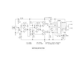
- 1. +5 - +12 VOLTS R1 10K C1 CD4538 + R10 C 10 µ f R6 _ 4 1M C3 .1 µ f C5 .1 µ f 9 1 16 1M 8 IC1C 2 15 NC R4 1 M R8 1M 10 D3 3 14 1 + 2 4 13 _ IC2 PIR 3 + 6 5 12 NO R2 1 7 + C6 3 IC1A + C4 IC1B 6 11 D5 100K D1 _ RY1 1µf 2 _ 10 5 13 14 D4 7 10 µf + IC1D 8 9 R3 D2 R5 12 10K + 11 Q1 10K R7 R9 2N3904 C2 + R11 10K 1M 1M R12 10 µ f 10K IC1 = LM324 PIR = PIR325 R10 Kohms X C6 mfd = ON time ms IC2 =CD4538 D1 - D5 = 1N914 RY1 - coil voltage rating = V+ voltage MOTION DETECTOR