Download to read offline

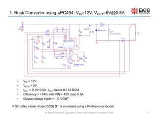


The document describes a buck converter design using a μPC494 controller. Key points: 1. The buck converter steps down 12V input to a regulated 5V, 0.5A output. Simulation results show output voltage regulation to within 1%, efficiency over 74%, and response to step loads within 250mV/250mA. 2. The design utilizes a Q2SA1680 MOSFET for switching and an XBS104V14R_P Schottky diode. Waveforms show current/voltage stresses and losses are analyzed based on device characteristics. 3. Operation is explained showing voltage control loop regulating output based on sensed voltage and PWM duty cycle control of switching transistor. Key components and their


