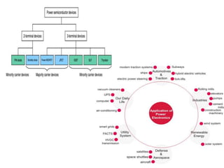
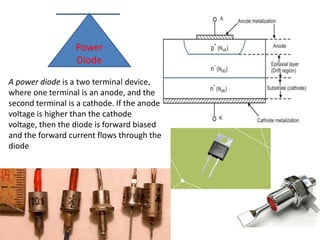
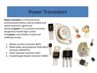
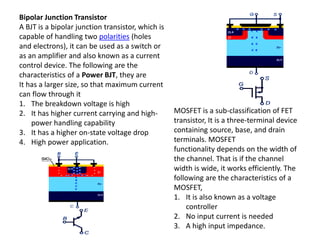
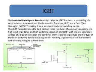
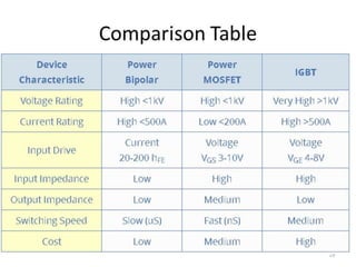
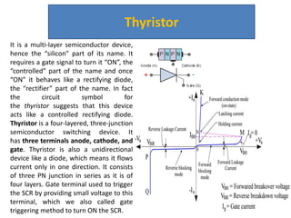
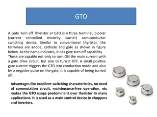
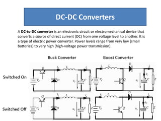
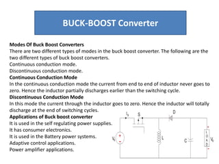
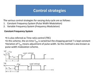
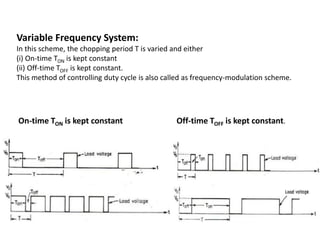
Power
Electronics
Shivani Mishra
Lecturer (EN)
Power Electronics in the Classical Era:
1.Mercury-Arc Rectifiers
The history of power electronics began with the invention of the glass-bulb pool-cathode
mercury-arc rectifier by the American inventor Peter Cooper Hewitt in 1902. While
experimenting with the mercury vapor lamp, which he patented in 1901, he found that
current flows in one direction only, from anode to cathode, thus giving rectifying action.
2.Hot-Cathode Gas Tube Rectifiers
The thyratron, or hot-cathode glass bulb gas tube rectifier, was invented by GE (1926) for
low-to-medium power applications. Functionally, it is similar to a grid-controlled
mercury-arc tube. Instead of a pool cathode, the thyratron tube used a dry cathode
thermionic emission heated by a filament similar to a vacuum triode, which was widely
used in those days.
3.Magnetic Amplifiers
Functionally, a magnetic amplifier (MA) is similar to a mercury-arc or thyratron rectifier.
Today it uses a high-permeability saturable reactor magnetic core with materials such as
Permalloy, Supermalloy, Deltamax, and Supermendur. A control winding with dc current
resets the core flux, whereas the power winding sets the core flux to saturate at a “firing
angle” and apply power to the load. The phase-controlled ac power could be converted
to variable dc with the help of a diode rectifier.
Power Electronics in the Modern
Era:
The modern solid-state electronics revolution
began with the invention of transistors in 1948
by Bardeen, Brattain, and Shockley of Bell
Laboratories. While Bardeen and Brattain
invented the point contact transistor, Shockley
invented the junction transistor. Although
solid-state electronics originally started with
Ge, it gradually transformed using with Si as its
base. The modern solid-state power
electronics revolution (often called the second
electronics revolution) started with the
invention of the p-n-p-n Si transistor in 1956
by Moll, Tanenbaum, Goldey, and Holonyak at
Bell Laboratories, and GE introduced the
thyristor (or SCR) to the commercial market in
1958.
Advantages of Semiconductor Devices
1. As semiconductor devices have no filaments, hence no power is needed to heat
them to cause the emission of electrons.
2. Since no heating is required, semiconductor devices are set into operation as soon as
the circuit is switched on.
3. During operation, semiconductor devices do not produce any humming noise.
4. Semiconductor devices require low voltage operation as compared to vacuum tubes.
5. Owing to their small sizes, the circuits involving semiconductor devices are very
compact.
6. Semiconductor devices are shock proof.
7. Semiconductor devices are cheaper as compared to vacuum tubes.
8. Semiconductor devices have an almost unlimited life.
9. As no vacuum has to be created in semiconductor devices, they have no vacuum
deterioration trouble.
Disadvantages of Semiconductor Devices
1. The noise level is higher in semiconductor devices as compared to that in the vacuum
tubes.
2. Ordinary semiconductor devices cannot handle as more power as ordinary vacuum
tubes can do.
3. In high frequency range, they have poor responder.
A power diode is a two terminal device,
where one terminal is an anode, and the
second terminal is a cathode. If the anode
voltage is higher than the cathode
voltage, then the diode is forward biased
and the forward current flows through the
diode
Power
Diode
Power transistor is a three terminal
semiconductor device used to amplify and
switch electronic signals and
electrical power. It is a junction transistor
designed to handle high current
and power; used chiefly in audio and
switching circuits.
Power Transistors
1. Bipolar junction transistor (BJTs)
2. Metal oxide semiconductor field-effect
transistor (MOSFETs)
3. Static induction transistor (SITs)
4. Insulated-gate bipolar transistor (IGBTs)
Bipolar Junction Transistor
A BJT is a bipolar junction transistor, which is
capable of handling two polarities (holes
and electrons), it can be used as a switch or
as an amplifier and also known as a current
control device. The following are the
characteristics of a Power BJT, they are
It has a larger size, so that maximum current
can flow through it
1. The breakdown voltage is high
2. It has higher current carrying and high-
power handling capability
3. It has a higher on-state voltage drop
4. High power application.
MOSFET is a sub-classification of FET
transistor, It is a three-terminal device
containing source, base, and drain
terminals. MOSFET
functionality depends on the width of
the channel. That is if the channel
width is wide, it works efficiently. The
following are the characteristics of a
MOSFET,
1. It is also known as a voltage
controller
2. No input current is needed
3. A high input impedance.
IGBT
The Insulated Gate Bipolar Transistor also called an IGBT for short, is something of a
cross between a conventional Bipolar Junction Transistor, (BJT) and a Field Effect
Transistor, (MOSFET) making it ideal as a semiconductor switching device.
The IGBT Transistor takes the best parts of these two types of common transistors, the
high input impedance and high switching speeds of a MOSFET with the low saturation
voltage of a bipolar transistor, and combines them together to produce another type of
transistor switching device that is capable of handling large collector-emitter currents
with virtually zero gate current drive.
MOSFET v/s IGBT
Thyristor
It is a multi-layer semiconductor device,
hence the “silicon” part of its name. It
requires a gate signal to turn it “ON”, the
“controlled” part of the name and once
“ON” it behaves like a rectifying diode,
the “rectifier” part of the name. In fact
the circuit symbol for
the thyristor suggests that this device
acts like a controlled rectifying diode.
Thyristor is a four-layered, three-junction
semiconductor switching device. It
has three terminals anode, cathode, and
gate. Thyristor is also a unidirectional
device like a diode, which means it flows
current only in one direction. It consists
of three PN junction in series as it is of
four layers. Gate terminal used to trigger
the SCR by providing small voltage to this
terminal, which we also called gate
triggering method to turn ON the SCR.
GTO
A Gate Turn off Thyristor or GTO is a three terminal, bipolar
(current controlled minority carrier) semiconductor
switching device. Similar to conventional thyristor, the
terminals are anode, cathode and gate as shown in figure
below. As the name indicates, it has gate turn off capability.
These are capable not only to turn ON the main current with
a gate drive circuit, but also to turn it OFF. A small positive
gate current triggers the GTO into conduction mode and also
by a negative pulse on the gate, it is capable of being turned
off.
Advantages like excellent switching characteristics, no need
of commutation circuit, maintenance-free operation, etc
makes the GTO usage predominant over thyristor in many
applications. It is used as a main control device in choppers
and inverters.
SCR Turn ON Methods –
1. Forward Voltage Triggering
2. Temperature Triggering
3. dv/dt Triggering
4. Light Triggering
5. Gate Triggering
• DC Gate Triggering
• AC Triggering
• Pulse Triggering
Parallel connection
Series Connection
The turn OFF process of an SCR is called commutation. The term commutation means
the transfer of currents from one path to another. So the commutation circuit does this
job by reducing the forward current to zero so as to turn OFF the SCR or Thyristor.
To turn OFF the conducting SCR the below conditions must be satisfied-
1. The anode or forward current of SCR must be reduced to zero or below the level of
holding current and then,
2. A sufficient reverse voltage must be applied across the SCR to regain its forward
blocking state.
SCR Turn OFF Methods
1. Natural Commutation
2. Forced Commutation
•Class A Commutation
•Class B Commutation
•Class C Commutation
•Class D Commutation
•Class E Commutation
SCR Turn OFF Methods
A DC-to-DC converter is an electronic circuit or electromechanical device that
converts a source of direct current (DC) from one voltage level to another. It is
a type of electric power converter. Power levels range from very low (small
batteries) to very high (high-voltage power transmission).
DC-DC Converters
BUCK-BOOST Converter
Modes Of Buck Boost Converters
There are two different types of modes in the buck boost converter. The following are the
two different types of buck boost converters.
Continuous conduction mode.
Discontinuous conduction mode.
Continuous Conduction Mode
In the continuous conduction mode the current from end to end of inductor never goes to
zero. Hence the inductor partially discharges earlier than the switching cycle.
Discontinuous Conduction Mode
In this mode the current through the inductor goes to zero. Hence the inductor will totally
discharge at the end of switching cycles.
Applications of Buck boost converter
It is used in the self regulating power supplies.
It has consumer electronics.
It is used in the Battery power systems.
Adaptive control applications.
Power amplifier applications.
Control strategies
The various control strategies for varying duty cycle are as follows:
1. Constant Frequency System (Pulse Width Modulation)
2. Variable Frequency System (Frequency Modulation)
Constant Frequency System
•It is also referred as Time-ratio control (TRC)
•In this scheme, the on-time TON is varied but the chopping period T is kept constant
•Variation of TON means adjustment of pulse width. So this method is also known as
pulse-width modulation scheme.
Variable Frequency System:
In this scheme, the chopping period T is varied and either
(i) On-time TON is kept constant
(ii) Off-time TOFF is kept constant.
This method of controlling duty cycle is also called as frequency-modulation scheme.
On-time TON is kept constant Off-time TOFF is kept constant.

Ppt on power electronics

  • 1.
  • 2.
    Power Electronics inthe Classical Era: 1.Mercury-Arc Rectifiers The history of power electronics began with the invention of the glass-bulb pool-cathode mercury-arc rectifier by the American inventor Peter Cooper Hewitt in 1902. While experimenting with the mercury vapor lamp, which he patented in 1901, he found that current flows in one direction only, from anode to cathode, thus giving rectifying action. 2.Hot-Cathode Gas Tube Rectifiers The thyratron, or hot-cathode glass bulb gas tube rectifier, was invented by GE (1926) for low-to-medium power applications. Functionally, it is similar to a grid-controlled mercury-arc tube. Instead of a pool cathode, the thyratron tube used a dry cathode thermionic emission heated by a filament similar to a vacuum triode, which was widely used in those days. 3.Magnetic Amplifiers Functionally, a magnetic amplifier (MA) is similar to a mercury-arc or thyratron rectifier. Today it uses a high-permeability saturable reactor magnetic core with materials such as Permalloy, Supermalloy, Deltamax, and Supermendur. A control winding with dc current resets the core flux, whereas the power winding sets the core flux to saturate at a “firing angle” and apply power to the load. The phase-controlled ac power could be converted to variable dc with the help of a diode rectifier.
  • 3.
    Power Electronics inthe Modern Era: The modern solid-state electronics revolution began with the invention of transistors in 1948 by Bardeen, Brattain, and Shockley of Bell Laboratories. While Bardeen and Brattain invented the point contact transistor, Shockley invented the junction transistor. Although solid-state electronics originally started with Ge, it gradually transformed using with Si as its base. The modern solid-state power electronics revolution (often called the second electronics revolution) started with the invention of the p-n-p-n Si transistor in 1956 by Moll, Tanenbaum, Goldey, and Holonyak at Bell Laboratories, and GE introduced the thyristor (or SCR) to the commercial market in 1958.
  • 4.
    Advantages of SemiconductorDevices 1. As semiconductor devices have no filaments, hence no power is needed to heat them to cause the emission of electrons. 2. Since no heating is required, semiconductor devices are set into operation as soon as the circuit is switched on. 3. During operation, semiconductor devices do not produce any humming noise. 4. Semiconductor devices require low voltage operation as compared to vacuum tubes. 5. Owing to their small sizes, the circuits involving semiconductor devices are very compact. 6. Semiconductor devices are shock proof. 7. Semiconductor devices are cheaper as compared to vacuum tubes. 8. Semiconductor devices have an almost unlimited life. 9. As no vacuum has to be created in semiconductor devices, they have no vacuum deterioration trouble. Disadvantages of Semiconductor Devices 1. The noise level is higher in semiconductor devices as compared to that in the vacuum tubes. 2. Ordinary semiconductor devices cannot handle as more power as ordinary vacuum tubes can do. 3. In high frequency range, they have poor responder.
  • 6.
    A power diodeis a two terminal device, where one terminal is an anode, and the second terminal is a cathode. If the anode voltage is higher than the cathode voltage, then the diode is forward biased and the forward current flows through the diode Power Diode
  • 7.
    Power transistor isa three terminal semiconductor device used to amplify and switch electronic signals and electrical power. It is a junction transistor designed to handle high current and power; used chiefly in audio and switching circuits. Power Transistors 1. Bipolar junction transistor (BJTs) 2. Metal oxide semiconductor field-effect transistor (MOSFETs) 3. Static induction transistor (SITs) 4. Insulated-gate bipolar transistor (IGBTs)
  • 8.
    Bipolar Junction Transistor ABJT is a bipolar junction transistor, which is capable of handling two polarities (holes and electrons), it can be used as a switch or as an amplifier and also known as a current control device. The following are the characteristics of a Power BJT, they are It has a larger size, so that maximum current can flow through it 1. The breakdown voltage is high 2. It has higher current carrying and high- power handling capability 3. It has a higher on-state voltage drop 4. High power application. MOSFET is a sub-classification of FET transistor, It is a three-terminal device containing source, base, and drain terminals. MOSFET functionality depends on the width of the channel. That is if the channel width is wide, it works efficiently. The following are the characteristics of a MOSFET, 1. It is also known as a voltage controller 2. No input current is needed 3. A high input impedance.
  • 9.
    IGBT The Insulated GateBipolar Transistor also called an IGBT for short, is something of a cross between a conventional Bipolar Junction Transistor, (BJT) and a Field Effect Transistor, (MOSFET) making it ideal as a semiconductor switching device. The IGBT Transistor takes the best parts of these two types of common transistors, the high input impedance and high switching speeds of a MOSFET with the low saturation voltage of a bipolar transistor, and combines them together to produce another type of transistor switching device that is capable of handling large collector-emitter currents with virtually zero gate current drive.
  • 10.
  • 11.
    Thyristor It is amulti-layer semiconductor device, hence the “silicon” part of its name. It requires a gate signal to turn it “ON”, the “controlled” part of the name and once “ON” it behaves like a rectifying diode, the “rectifier” part of the name. In fact the circuit symbol for the thyristor suggests that this device acts like a controlled rectifying diode. Thyristor is a four-layered, three-junction semiconductor switching device. It has three terminals anode, cathode, and gate. Thyristor is also a unidirectional device like a diode, which means it flows current only in one direction. It consists of three PN junction in series as it is of four layers. Gate terminal used to trigger the SCR by providing small voltage to this terminal, which we also called gate triggering method to turn ON the SCR.
  • 12.
    GTO A Gate Turnoff Thyristor or GTO is a three terminal, bipolar (current controlled minority carrier) semiconductor switching device. Similar to conventional thyristor, the terminals are anode, cathode and gate as shown in figure below. As the name indicates, it has gate turn off capability. These are capable not only to turn ON the main current with a gate drive circuit, but also to turn it OFF. A small positive gate current triggers the GTO into conduction mode and also by a negative pulse on the gate, it is capable of being turned off. Advantages like excellent switching characteristics, no need of commutation circuit, maintenance-free operation, etc makes the GTO usage predominant over thyristor in many applications. It is used as a main control device in choppers and inverters.
  • 13.
    SCR Turn ONMethods – 1. Forward Voltage Triggering 2. Temperature Triggering 3. dv/dt Triggering 4. Light Triggering 5. Gate Triggering • DC Gate Triggering • AC Triggering • Pulse Triggering
  • 14.
  • 15.
    The turn OFFprocess of an SCR is called commutation. The term commutation means the transfer of currents from one path to another. So the commutation circuit does this job by reducing the forward current to zero so as to turn OFF the SCR or Thyristor. To turn OFF the conducting SCR the below conditions must be satisfied- 1. The anode or forward current of SCR must be reduced to zero or below the level of holding current and then, 2. A sufficient reverse voltage must be applied across the SCR to regain its forward blocking state. SCR Turn OFF Methods 1. Natural Commutation 2. Forced Commutation •Class A Commutation •Class B Commutation •Class C Commutation •Class D Commutation •Class E Commutation SCR Turn OFF Methods
  • 16.
    A DC-to-DC converteris an electronic circuit or electromechanical device that converts a source of direct current (DC) from one voltage level to another. It is a type of electric power converter. Power levels range from very low (small batteries) to very high (high-voltage power transmission). DC-DC Converters
  • 17.
    BUCK-BOOST Converter Modes OfBuck Boost Converters There are two different types of modes in the buck boost converter. The following are the two different types of buck boost converters. Continuous conduction mode. Discontinuous conduction mode. Continuous Conduction Mode In the continuous conduction mode the current from end to end of inductor never goes to zero. Hence the inductor partially discharges earlier than the switching cycle. Discontinuous Conduction Mode In this mode the current through the inductor goes to zero. Hence the inductor will totally discharge at the end of switching cycles. Applications of Buck boost converter It is used in the self regulating power supplies. It has consumer electronics. It is used in the Battery power systems. Adaptive control applications. Power amplifier applications.
  • 18.
    Control strategies The variouscontrol strategies for varying duty cycle are as follows: 1. Constant Frequency System (Pulse Width Modulation) 2. Variable Frequency System (Frequency Modulation) Constant Frequency System •It is also referred as Time-ratio control (TRC) •In this scheme, the on-time TON is varied but the chopping period T is kept constant •Variation of TON means adjustment of pulse width. So this method is also known as pulse-width modulation scheme.
  • 19.
    Variable Frequency System: Inthis scheme, the chopping period T is varied and either (i) On-time TON is kept constant (ii) Off-time TOFF is kept constant. This method of controlling duty cycle is also called as frequency-modulation scheme. On-time TON is kept constant Off-time TOFF is kept constant.