Resonance frequency analysis of laser optical fiber based on microcantileverIJECEIAES
The normal frequency of smart beams was originated utilizing FEM [Ansys and Comsol] code for first five modes by varying the position of actuator from the fixed end of the structure, and it has a suitable arrangement with analytically found the standard frequency. This paper includes learning a resonance frequency analysis of laser optical fiber based on microcantilever of designing magnetic actuator using Ansys and Comsol simulation. The design of optical fiber includes Nickel cantilever, two magnets and one coil that apply to force on the cantilever. After the current flows in the coil domain, the shape of microcantilever will be deformed. It will move to z- direction that depends on the force direction. Two methods including, Comsol Multiphysics, Ansys and analytical equations have been utilized to calculate the resonance frequency, current and force values. The simulation results include calculating the current (magnetic current density) and effects of the magnetic field of the coil on the cantilever (force calculation). Utilizing this method is to limit faults(errors) of optical fiber laser between transmitter and receiver system (detection system) for any time of cutting coil when the signal of a laser passes through the coil. In conculsions, resonant frequency (f_n) tuning using cantilivier presented in the resrach have larger variable range by using simulations. However,the adjusting of the system and changing the deminsions.Resolutions to this problematic contain tuning the modes of resonant frequency to produce by cantilivier with 2-magnets and coil when the signal pass from laser source. Based on these simulations and characterization results, the proposed assembly can be a good applicant for evolving a low price, high material platform for many biological, laser optical fiber, communication, machine learning, biosensors and biomedical applications.
Plenary lecture given by Prof. Kenneth Gonsalves (ITT Mandi, India) on September 12, 2017 in Gramado (Brazil) during the XVI B-MRS Meeting. Acknowledgment: ITT Mandi.
GEOMETRY AND CHARACTERIZATION OF LOW INDEX SILICON MICRO RING RESONATORSoptljjournal
An optical ring resonator is indeed a series of waveguides in which a closed loop coupled with some sort of input and output of light is at least one. The consequence of the index difference on dielectric waveguide characteristics such as single-mode process, losses, efficiency of fiber to waveguide coupling, minimum bending radius, hybridity mode, birefringence, polarization effects, repeatability and stability, integration
size, realizable circuits, technical constraints and usable materials is indeed very significant for study. The purpose of this article is to analyze the effect of the features of the waveguide with regard to the index correlation and to explore the difficulties. This article assesses the effect of the intensity index on the characteristics of the dielectric waveguide, such as the single-mode device, losses, technical constraints and materials available. This work is an approximation for the design of optical waveguides, so that by lowering the silicon index, we can achieve versatility
PolyMEMS INAOE, a Surface Micromachining Fabrication Module and the Developm...José Andrés Alanís Navarro
The PolyMEMS INAOE module for surface micromachining has been developed for the fabrication of electrostatic and electrothermal (Joule effect) sensors and actuators. In this module the designer can choose up to 3 Poly silicon layers and aluminum as electrical interconnecting material. A
micromechanical test chip has been fabricated which includes the following. a) Micro test structures for residual stress measurement; cantilever beams, clamped-clamped beams, ring-and-beam structures, diamond-and-beam structures, rotation beams, Vernier gauges, cantilever spirals, double-clamped microgauge, and b) Actuators; torsion and bending mirrors, resonators, single two-arms Joule structures (STA), chevron-like Joule arrays, capacitive array for accelerometers. In this work we are presenting the measured residual stress on our process, by using the clamped-clamped beam and ring-and-beam arrays. The measured compressive stress is in the 21-26 MPa range for both types of microgauges. A maximum typical value for this tensile stress is 50 MPa, which is higher than that obtained in our experimental procedure. From this residual stress measurement technique and other mechanical testing routines we can conclude the following: the thermal load, the polysilicon microstructure, and the releasing technique; all of them result in a reliable process for the fabrication of dynamic and static polysilicon microstructures.
Optimization of multijunction solar cell by wafer ray tracer for development ...eSAT Journals
Abstract Optical losses limit the excess carriers generation in absorber part of multijuction (MJ) solar cell. The generation of excess carriers is directly proportional to photogenerated current solar cell. Therefore, reduction of optical losses is fundamentally important for improving the power conversion efficiency. Thickness of layers strongly influences the performance of MJ solar cell. In this study we simulated a MJ solar cell of Air/ZnO/SiC/c-Si/a-Si(n)/Al structure using Wafer Ray Tracer (WRT) simulation software and optimized the thicknesses of the layers for photogenerated current. The simulation result shows that without SiC layer, only 57.48% of incident light is absorbed and generates 26.85 mA/cm2 photogenerated current in solar cell. A 70 nm thickness of optimized SiC layer is increasing the light absorption 22.16% and photogenerated current 38.54%. Result shows that there is no transmission of light through the absorber layer. The MJ solar cell without Back Surface Field (BSF) layer of a-Si(n) shows photogenerated current of 37.05 mA/cm2 which can be improved to 37.24 mA/cm2 with a 100 nm thickness of a-Si(n). The c-Si absorber layer shows highest absorptance within 500 nm-1000 nm wavelength of light spectrum with 100 nm thickness of a-Si(n). An a-Si(n) BSF layer at the back surface minimizes the effective back-surface recombination velocity and improves the collection probability of minority carriers of solar cell. Furthermore a 100 nm Al rear contact improves the photogenerated current of MJ solar cell to 37.25 mA/cm2. An Al rear contact layer improves the mechanical strength of c-Si absorber layer. The electrical property of Al improves the excess carriers’ collection probability of MJ solar cell. Keywords: Wafer Ray Tracer, Simulation, Multijunction Solar Cell, Photogeneration, Back Surface Field.
Design of a Selective Filter based on 2D Photonic Crystals Materials IJECEIAES
Two dimensional finite differences temporal domain (2D-FDTD) numerical simulations are performed in cartesian coordinate system to determine the dispersion diagrams of transverse electric (TE) of a two-dimension photonic crystal (PC) with triangular lattice. The aim of this work is to design a filter with maximum spectral response close to the frequency 1.55 μm. To achieve this frequency, selective filters PC are formed by combination of three waveguides W 1 K A wherein the air holes have of different normalized radii respectively r 1 /a=0.44, r 2 /a=0.288 and r /a= 0.3292 (a: is the periodicity of the lattice with value 0.48 μm). Best response is obtained when we insert three small cylindrical cavities (with normalized radius of 0.17) between the two half-planes of photonic crystal strong lateral confinement.
The radio frequency microelectromechanical system (RF MEMS) Materials Jitendra Jangid
RF technologies. Besides RF MEMS technology, III-V compound semiconductor (GaAs, GaN, InP, InSb), ferrite, ferroelectric, silicon-based semiconductor (RF CMOS, SiC and SiGe), and vacuum tube technology are available to the RF designer. Each of the RF technologies offers a distinct trade-off between cost, frequency, gain, large-scale integration, lifetime, linearity, noise figure, packaging, power handling, power consumption, reliability, ruggedness, size, supply voltage, switching time and weight.
Silicon photonics is an evolving technology in which data is transferred among computer chips by optical rays. Optical rays can carry far more data in less time than electrical conductors.
This presentation gives emphasis on the basics of silicon photonics
CIGS solar cells are one of the leading thin film solar cells to be made commercially viable. There are a lot of ways in manufacturing it and we have specialized a two stage process which gives advantages over material growth during commercial manufacture. An advancement of the two stage process is done to increase the throughput and maximize profits. A lab scale emulation of the commercial process is done to study device performance as a result of the advanced process. Factors such as reproducibility and elemental optimization were a concern and the reason behind these concerns were researched. This thesis serves as an experimental test bed to study device performance before up-scaling the growth recipe for pilot production.
Research results reveal that by 2020, an important amount of transactions will be handled with automated agents. Invest in digital agents now, before it's too late!
An impactful approach to the Seven Deadly Sins you and your Brand should avoid on Social Media! From a humoristic approach to a modern-life analogy for Social Media and including everything in between, this deck is a compelling resource that will provide you with more than a few take-aways for your Brand!
Programming Optical Circuits for Specific Applications and Reducing Productio...Abacus Technologies
Silicon photonics is an evolving technology which transfers data among computer chips by using optical rays which can carry far more data in less time than electrical conductors. The concept involves combining laser and silicon technology on a single chip, a silicon photonic chip.
It is a hugely promising developing area of technology that saw impressive growth last year, with more than 3.5 million silicon photonic transceivers for data centers having being shipped, yielding revenues of around $364 million. From now until 2026, Global Market Insights expects the silicon photonics market to grow at over 30% year-on-year to a value of over $3 billion.
A micro-electromechanical system (MEMS) gyroscope is commonly used to monitor the angular rate of a moving body due to its benefits. The most promising advantages include its small size, low cost, and a high degree of integration. MEMS gyroscope has different fabrication processes and micromachining techniques. LIGA (Lithography-Galvanoformung-Abformung), bulk micromachining, surface micromachining, Silicon-on-glass (SOG) and Deep Reactive Ion Etching (DRIE) are the known fabrication techniques for MEMS gyroscope. This paper systematically reviewed the fabrication techniques used to fabricate the MEMS gyroscope. The current review paper also focuses on the performance of MEMS gyroscope which included several recent developments. For the conclusion of results, the variable typically used is the rate of turn (°/s) for MEMS angular rate sensors with respect to bandwidth frequency. Finally based on the review some analysis on fabrication technology, key principles, and performance parameters are discussed.
Time Domain Modelling of Optical Add-drop filter based on Microcavity Ring Re...iosrjce
IOSR Journal of Electronics and Communication Engineering(IOSR-JECE) is a double blind peer reviewed International Journal that provides rapid publication (within a month) of articles in all areas of electronics and communication engineering and its applications. The journal welcomes publications of high quality papers on theoretical developments and practical applications in electronics and communication engineering. Original research papers, state-of-the-art reviews, and high quality technical notes are invited for publications.
EVALUATION OF OPTICALLY ILLUMINATED MOSFET CHARACTERISTICS BY TCAD SIMULATIONVLSICS Design
In this paper we report effect of optical illumination on Silicon MOSFET. The MOSFET has been studied in respect of current voltage, transconductance admittance and scattering parameters. Gain analysis of the Silicon MOSFET is done in dark and under optical illumination. The device is fabricated using ATHENA™ process simulator and the device simulation is performed using ATLAS™ from SILVACO international. The simulation results indicate potential of MOSFET as optically sensitive structure which can be used for increase in data transmission/reception rates, reduction of interconnect delays, elimination of clock skew, or as a photodetector for optoelectronic applications at low and radio frequency.
EVALUATION OF OPTICALLY ILLUMINATED MOSFET CHARACTERISTICS BY TCAD SIMULATIONVLSICS Design
In this paper we report effect of optical illumination on Silicon MOSFET. The MOSFET has been studied in
respect of current voltage, transconductance admittance and scattering parameters. Gain analysis of the
Silicon MOSFET is done in dark and under optical illumination. The device is fabricated using ATHENA™
process simulator and the device simulation is performed using ATLAS™ from SILVACO international.
The simulation results indicate potential of MOSFET as optically sensitive structure which can be used
for increase in data transmission/reception rates, reduction of interconnect delays, elimination of clock
skew, or as a photodetector for optoelectronic applications at low and radio frequency.
1. Mandar Deshpande UIC PHD PROJECTS
E-mail: deshmand@yahoo.com
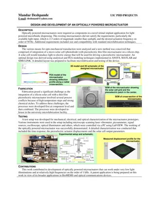
DESIGN AND DEVELOPMENT OF AN OPTICALLY POWERED MICROACTUATOR
DESCRIPTION
Optically powered microactuators were required as components in a novel retinal implant application for light
powered microfluidic dispensing. The existing microactuators did not satisfy the requirements; particularly the
available light input, which is 2-3 orders of magnitude smaller than sunlight, and the desired actuation frequency on
order of 50 Hz. Additional requirements included size and compatibility with standard microfabrication techniques.
DESIGN
The various means for opto-mechancial transduction were analyzed and a new method was conceived that
comprised of integration of a micro-solar cell (photodiode) with piezoelectric thin film microactuator on a silicon chip.
A solar cell would transduce light to electric energy that will be used for driving a piezoelectric microactuator. An
optimal design was derived using analytical and FEA modeling techniques implemented in ANSYS, MATLAB and
SIMULINK. A detailed layout was prepared to facilitate microfabrication and testing of the device.
FEA model of the
microactuator
showing deflection
profile along a radial
cross-section.
3D model and 2D schematic of the
designed microactuator
FABRICATION
Fabrication posed a significant challenge as the
integration of a silicon solar cell with a thin film
piezoelectric microactuator involved several process
conflicts because of high temperature steps and strong
chemical etches. To address these challenges, the
processes were developed first at component level and
then combined. The processes were developed in-
house in the university microfabrication facility.
SEM of the microactuator showing
the solar cell grid and the
piezoelectric patch in the center.
SEM of cross-section of the
microactuator.
TESTING
A test setup was developed for mechanical, electrical, and optical characterization of the microactuator prototypes.
Various instruments were used in the setup including microscope scanning laser vibrometer, picoammeter, signal
sources, oscilloscope, optical illuminators and others, which were controlled via a PC using LabVIEW. The working of
the optically powered microactuator was successfully demonstrated. A detailed characterization was conducted that
included the time response, the piezoelectric actuator displacements and the solar cell output parameters.
Experimental setup and schematic.
Measured displacement profile for the
microactuator.
CONTRIBUTIONS
This work contributed to development of optically powered microactuators that can work under very low light
illuminations and at relatively high frequencies on the order of 1 kHz. A patent application is being prepared on this
work in view of its broader applications in BioMEMS and optical communications devices.
2. Mandar Deshpande UIC PHD PROJECTS
E-mail: deshmand@yahoo.com
MICROFABRICATION OF AN OPTICALLY POWERED MICROACTUATOR
DESCRIPTION
An optically powered microactuator was proposed that integrated a micro-solar cell with a piezoelectric
microactuator on a single silicon chip. The integration of the two devices through microfabrication posed significant
challenges in form of deposition conditions for good quality PZT (Lead Zirconate Titanate) thin film, DRIE process
development for diaphragm etching, and process conflicts because of high temperatures processes and strong
chemical etches.
PROCESS DEVELOPMENT
To systematically address the challenges the process development was undertaken at the component level first,
where the micro-solar cell and the piezoelectric microactuator were fabricated and tested separately. After successful
component development, the fabrication processes were appropriately combined to fabricate the integrated actuator.
Process Description
(a) Alignment mark (Photolithography and RIE)
(b) Oxide dopant mask (oxidation and photolithography)
(c)-(e) Doping of phosphorus into silicon (Spin on dopant, diffusion and
dry oxidation)
(f) Bottom electrodes for PZT (Photolithography, e-beam deposition, Lift-
off)
(g) PZT thin film via sol gel method (CSD, photolithography, wet-etching,
RTP)
(h) Oxide etching for ohmic contact (photolithography, BOE etch)
(i) Top electrode forming the solar cell grid (Photolithography, e-beam
deposition, Lift-off)
(j)-(l) Diaphragm by backside etching using DRIE (Photolithography,
Backside alignment, Thick photoresist, Bosch Process)
Key Processes Developed
1. Deposition parameters for Pt/Ti film to lower stress buildup
2. PZT thin film sol-gel process – Pyrolisis temperature and RTP profile
to eliminate peeling/cracking of PZT film.
3. PZT thin film wet etch – New etch recipe that reduced undercut and
showed high selectivity over oxide.
4. Thick photoresist processing (SPR-220-7.0) – improved process recipe
that eliminated cracking problem for a 20 µm thick resist film.
5. DRIE parameters for etching large area silicon – ICP parameters for
straight side wall profile for exposed area in the millimeter scale.
Images of
a device
during
fabrication
steps.
Alignment Oxide mask Doped Si Pt/Ta electrode PZT Thin film Oxide etch Au/Ti electrode DRIE
RESULTS
Working prototypes were successfully fabricated and tests showed satisfactory operation with reference to the
desired requirements. This work contributed to developing a method for incorporating a solar cell with a
conventional MEMS device to create optically powered MEMS.
Processed wafer before dicing. SEM of a microactuator device.
SEM images of cross-section showing constituent
layers and the etched silicon diaphragm
3. Mandar Deshpande UIC PHD PROJECTS
E-mail: deshmand@yahoo.com
MEASUREMENT OF PROPERTIES OF PIEZOELECTRIC THIN FILMS ON MICROACTUATORS
DESCRIPTION
Accurate values of piezoelectric properties are useful for evaluating piezoelectric microactuators and tailoring
their performance for various applications. There are several challenges with regards to measuring these properties.
They cannot be measured directly and show significant variations with compositions, type of substrates, processing
conditions and the driving voltage. Many new indirect measurement methods are being developed, but most require
fabrication of specialized structures such as cantilevers, or provide properties measured under sensor mode, which
does no reflect its behavior under actuation mode. In this work a method was developed that allowed for non-
destructive and accurate measurement of the piezoelectric properties under practical actuation conditions.
APPROACH
The method involved developing a finite element (FE) model of the microactuator and structurally validating it
by corroborating the resonance frequencies and modes with measurements. Following this, the piezoelectric
properties in the FE model were adjusted to match the measured deflections, thus providing an accurate estimate of
the properties as a function of the applied voltage.
To validate the method, square piezoelectric microactuators were fabricated using KOH etched silicon
diaphragms and PZT thin films. Next, first 8 resonance modes and frequencies were measured using a microscope
laser scanning vibrometer and were used for validating a FE model built in ANSYS. The piezoelectric properties
were then computed by comparing the FE results with the measured deflections.
Microactuator fabrication process
Oxidation - LPVCD Nitride - Photolith -
RIE patterning - KOH - Photolith - e-
beam Pt/Ti - Liftoff - PZT sol gel -
Photolith - Wet-etch - RTP- Photolith -
e-beam Ag/Cr - Liftoff.
Fabricated microactuator. Experimental setup for measuring mode shapes and
deflections.
Cross-section showing
KOH etched silicon
diaphragm.
FE Model of the
microactuator.
Experimental and FEM mode shapes and
frequencies showing excellent corroboration. The transverse piezoelectric properties
as a function of the applied voltage.
RESULTS AND CONTRIBUTIONS
The piezoelectric properties were shown to be a function of the applied voltage, with the values at higher
voltages corroborating with the results published in other studies. These results showed that at low voltages the
effective properties are significantly lower than that published in most studies.
4. Mandar Deshpande UIC PHD PROJECTS
E-mail: deshmand@yahoo.com
OTHER MEMS PROJECTS
FABRICATION OF A COMPLIANT MEMS MANIPULATOR
A project required microfabrication of a silicon
compliant mechanism for manipulation of microscale
objects. The design called for a millimeter scale frame
structure with thickness of 20 µm. DRIE process on an
SOI wafer was selected as the best approach for
achieving the desired structure.
A COMB-DRIVE BASED CORIOLIS FLOW RATE SENSOR
In order to address the lack of MEMS flow rate
sensors that can be integrated on a chip with microfluidic
circuitry, a novel comb drive based flow rate sensor
operating using the coriolis principle was designed. In
this sensor the flow was directed through the supporting
beams of the comb-drive, which would bend during
motion because of coriolis force in proportion to the
mass flow rate.
A fabrication process was devised that allowed for
on-chip fabrication of the comb drive sensor and the
microfluidic connecting channels. The sensor showed
high sensitivity with a theoretical resolution of less than
1 µL/s for water.
SEM of millimeter scale complaint mechanism fabricated
on a SOI substrate
CAD drawing of the designed device
AN ANALYTICAL MODEL FOR CIRCULAR PIEZOELECTRIC MICROACTUATORS
DESCRIPTION
Circular bending type piezoelectric actuators are widely used in MEMS for applications such as ultrasonic
devices, pumps and others. The deflections generated by these actuators are sensitive to the relative dimensions of
the constitutive structural components such as the substrate and the piezoelectric layer. An analytical model leading
to a closed form equations has been long desired for convenient design optimization of the actuators, but has been
difficult to derive because of the multilayered and non-homogenous structure of the actuator.
METHOD
An analytical model was derived using Classical Laminated Plate Theory and closed form equations were found
for the deflections of circular piezoelectric actuators under voltage and pressure loading conditions. The equations
were validated via corroboration with experiments and FE model, and a high accuracy within 96.5 % of the
experimental results was obtained.
Analytical framework for CLPT
derivation. Computed deflections in FE.
Experimental setup and the test actuator.