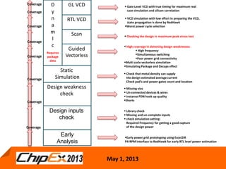
May 1, 2013
PDN (Power Delivery Network)
verification flow
Power, Noise, and Reliability Analyses for
Advanced Electronic Systems
Ronen Stilkol
ronen.stilkol@ansys.com
May 1, 2013
PDN verification requirements
5/25/2013, 2
 High design failure coverage
Early detection of design faults and weaknesses
Early prototyping and grid planning
Failure root cause analysis to improve productivity
Full integration of Board, Package and Die effects
©2009 Apache Design Solutions, Confidential and Proprietary
May 1, 2013
 Missing vias
 Un-connected devices & wires
 Instance PDN hook up quality
Shorts
Design weakness
check
 Check that metal density can supply
the design estimated average current
Check pad’s and power gates count and location
Static
Simulation
 Checking the design in maximum peak stress test
Scan
RTL VCD  VCD simulation with low effort in preparing the VCD,
state propagation is done by RedHawk
Worst power cycle selection
 Gate Level VCD with true timing for maximum real
case simulation and silicon correlation
GL VCD
 High coverage in detecting design weaknesses:
 High frequency
Simultaneous switching
Poor power grid connectivity
Multi cycle vectorless simulation
Simulating Package and Decaps effect
Guided
Vectorless
D
y
n
a
m
I
c
Requires
package
data
Coverage
 Library check
 Missing and un-complete inputs
 check simulation setting:
Required Frequency for getting a good capture
of the design power
Design inputs
check
Coverage
Coverage
Coverage
Coverage
Coverage
Coverage
Early
Analysis
Early power grid prototyping using Excel2IR
PA RPM interface to RedHawk for early RTL level power estimation
Coverage

TRACK C: PDN (Power Delivery Network)/ Ronen Stilkol

  • 1.
    May 1, 2013 PDN(Power Delivery Network) verification flow Power, Noise, and Reliability Analyses for Advanced Electronic Systems Ronen Stilkol ronen.stilkol@ansys.com
  • 2.
    May 1, 2013 PDNverification requirements 5/25/2013, 2  High design failure coverage Early detection of design faults and weaknesses Early prototyping and grid planning Failure root cause analysis to improve productivity Full integration of Board, Package and Die effects ©2009 Apache Design Solutions, Confidential and Proprietary
  • 3.
    May 1, 2013 Missing vias  Un-connected devices & wires  Instance PDN hook up quality Shorts Design weakness check  Check that metal density can supply the design estimated average current Check pad’s and power gates count and location Static Simulation  Checking the design in maximum peak stress test Scan RTL VCD  VCD simulation with low effort in preparing the VCD, state propagation is done by RedHawk Worst power cycle selection  Gate Level VCD with true timing for maximum real case simulation and silicon correlation GL VCD  High coverage in detecting design weaknesses:  High frequency Simultaneous switching Poor power grid connectivity Multi cycle vectorless simulation Simulating Package and Decaps effect Guided Vectorless D y n a m I c Requires package data Coverage  Library check  Missing and un-complete inputs  check simulation setting: Required Frequency for getting a good capture of the design power Design inputs check Coverage Coverage Coverage Coverage Coverage Coverage Early Analysis Early power grid prototyping using Excel2IR PA RPM interface to RedHawk for early RTL level power estimation Coverage