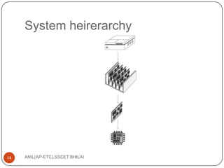
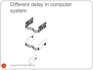
Algorithms for VLSI Physical
Design Automation (ME-III SEM)
prepared by :
ANIL KUMAR SAHU(Assistant Professor,
SSCET)

1

ANIL(AP-ETC),SSCET BHILAI
 Partitioning
 Efficient designing of any complex system

necessitates decomposition of the same into a set of
smaller subsystems. Subsequently,
 each subsystem can be designed independently and
simultaneously to speed up the design process.
 The process of decomposition is called partitioning.
Partitioning efficiency can be enhanced within three
broad parameters.
 First of all, the system must be design time.

2

ANIL(AP-ETC),SSCET BHILAI
 decomposed carefully so that the original functionality

of the system remains intact.
 Secondly, an interface specification is generated
during the decomposition ,which is used to connect all
the subsystems.
 The system decomposition should ensure
minimization of the interface interconnections
between any two subsystems.
 Finally, the decomposition process should be simple
and efficient so that the time required for the
decomposition is a small fraction of the total
3

ANIL(AP-ETC),SSCET BHILAI
 Further partitioning may be required in the events

4

where the size of a subsystem remains too large to be
designed efficiently.
 Thus, partitioning can be used in a hierarchical
manner until each subsystem created has a
manageablesize.
 Partitioning is a general technique and finds
application in diverse areas.
 For example, in algorithm design, the divide and
conquer approach is routinely used to partition
complex problems into smaller and simpler problems.
 The increasing popularity of the parallel computation
techniques brings in its fold promises in terms of
provision of innovative tools for solution of complex
problems,
ANIL(AP-ETC),SSCET BHILAI
 by combining partitioning and parallel processing
techniques.
 Partitioning plays a key role in the design of a







5

computer system in general,
and VLSI chips in particular.
A computer system is comprised of tens of millions of
transistors. It is partitioned into several smaller
modules/blocks for facilitation of the design process.
Each block has terminals located at the periphery that
are used to connect the blocks.
The connection is specified by a netlist, which is a
collection of nets. A net is a set of terminals which
have to be made electrically equivalent.
Figure 5.1 (a) shows a circuit, which has been
partitioned into three subcircuits.
Note that the number of interconnections between
any two partitions is four (as shown in Figure 5.1(b)).

ANIL(AP-ETC),SSCET BHILAI
 A VLSI system is partitioned at several levels due

6

to its complexity.
 The partitioning of a system into a group of PCBs
is called the system level
 partitioning. The partitioning of a PCB into chips is
called the board level
 partitioning while the partitioning of a chip into
smaller subcircuits is called the chip level
partitioning.
 At each level, the constraints and objectives of
the partitioning process are different as discussed
ANIL(AP-ETC),SSCET BHILAI
below.
 The circuit assigned to a PCB must satisfy certain

constraints. Each PCB usually has a fixed area, and a
fixed number of terminals to connect with other boards.
 The number of terminals available in one board
(component) to connect to other boards (components) is
called the terminal count of the board (component).
 For example, a typical board has dimensions 32 cm×15
cm and its terminal count is 64. Therefore, the subcircuit
allocated to a board must be manufacturable within the
dimensions of the board.
 In addition, the number of nets used to connect this board
to the other boards must be within the terminal count of the
board.

System Level Partitioning
7

ANIL(AP-ETC),SSCET BHILAI
 The reliability of the system is inversely proportional







8

to the number of boards in the system.
Hence, one of the objectives of partitioning is to
minimize the number of boards.
Another important objective is the optimization of the
system performance.
Partitioning must minimize any degradation of the
performance caused by the delay due to the
connections between components on different
boards.
The signal carried by a net that is cut by partitioning
at this level has to travel from one board to another
board through the system bus.
The system bus is very slow as the bus has to
adhere to some strict specifications so that a variety

ANIL(AP-ETC),SSCET BHILAI
 of different boards can share the same bus.
 The delay caused by signals traveling between PCBs

(off-board delay) plays a major role in determining the
system performance as this delay is much larger than
the on-board or the on-chip delay.

9

ANIL(AP-ETC),SSCET BHILAI
Partitioning of circuit

10

ANIL(AP-ETC),SSCET BHILAI
 The board level partitioning faces a different set of







constraints and fulfills a different set of objectives as
opposed to system level partitioning.
Unlike boards, chips can have different sizes and can
accommodate different number of terminals.
Typically the dimensions of a chip range from 2 mm×2 mm
to 25 mm×25 mm.
The terminal count of a chip depends on the package of
the chip.
A Dual
In-line Package (DIP) allows only 64 pins while a Pin Grid
Array (PGA) package may allow as many as 300 pins.

Board Level Partitioning:
11

ANIL(AP-ETC),SSCET BHILAI
 While system level partitioning is geared towards

12

satisfying the area and the terminal constraints of
each partition,
 board level partitioning ventures to minimize the
area of each chip.
 The shift of emphasis is attributable to the cost of
manufacturing a chip that is proportional to its
 area.
 In addition, it is expedient that the number of
chips used for each board be minimized for
enhanced board reliability.
ANIL(AP-ETC),SSCET BHILAI the
 Minimization of
 number of chips is another important determinant of

13

performance because the off-chip delay is much
larger than the on-chip delay.
 This differential in delay arises because the distance
between two adjacent transistors on a chip is a few
while the distance between two adjacent chips is in
mm.
 In addition to traversing a longer distance, the signal
has to travel between chips, and through the
connector.
 The connector used to attach the chip to the board
typically has a high resistance and contributes
significantly to the signal delay.
 Figure 5.3 shows the different kinds of delay in a
computer system. In Figure 5.3(b), the off-board delay
is compared with
ANIL(AP-ETC),SSCET BHILAI the on-board delay while the off-chip
delay is compared with the on-chip delay in Figure
System heirerarchy

14

ANIL(AP-ETC),SSCET BHILAI
Different delay in computer
system

15

ANIL(AP-ETC),SSCET BHILAI
 The circuit assigned to a chip can be fabricated as

a single unit, therefore, partitioning at this level is
necessary.
 A chip can accommodate as many as three million or
more transistors. The fundamental objective of chip
level partitioning is to facilitate efficient design of the
chip.
 After partitioning, each sub circuit, which is also called
a block, can be designed independently using either
full custom or standard cell design style.
 Since partitioning is not constrained by physical
dimensions, there is no area constraint for any
partition. However, the partitions may be restrained by
user specified area constraints for optimization of the
design Level
Chip process. Partitioning

16

ANIL(AP-ETC),SSCET BHILAI
 The terminal count for a partition is given by the

17

ratio of the perimeter of the partition to the
terminal pitch.
 The minimum spacing between two adjacent
terminals is called terminal pitch and is
determined by the design rules. The number of
nets which connect a partition to other
 partitions cannot be greater than the terminal
count of the partition.
 In addition, the number of nets cut by partitioning
should be minimized to simplify the routing task.
 The minimization of the number of nets cut by
partitioning is one of the most important
ANIL(AP-ETC),SSCET BHILAI
objectives in partitioning.
 The terminal count for a partition is given by the ratio of the

18

perimeter
 of the partition to the terminal pitch. The minimum spacing
between
 two adjacent terminals is called terminal pitch and is
determined by the
 design rules. The number of nets which connect a partition
to other
 partitions cannot be greater than the terminal count of the
partition. In
 addition, the number of nets cut by partitioning should be
minimized to
 simplify the routing task. The minimization of the number of
nets cut
ANIL(AP-ETC),SSCET BHILAI
 by partitioning is one of the most important objectives in
partitioning.
 A disadvantage of the partitioning process is that it may degrade the

performance of the final design. Figure 5.4(a) shows two components
A and B which are critical to the chip performance, and therefore, must
be placed close together.
 However, due to partitioning, components A and B may be assigned to

different partitions and may appear in the final layout as shown in Figure
5.4(b).
 it is easy to see that the connection between A and B is very long,

leading to a very large delay and degraded performance.
 Thus, during partitioning, these critical components should be assigned

to the same partition. If such an assignment is not possible,
 Then appropriate timing constraints must be generated to keep the two

critical components close together. Chip performance is determined by
several components forming a critical path. Assignment of these
components to different partitions extends the length of the critical path.
 Thus, a major challenge for improvement of system performance is
19

ANIL(AP-ETC),SSCET BHILAI
minimization of the length

of critical path.
20

ANIL(AP-ETC),SSCET BHILAI
 At any level of partitioning, the input to the partitioning algorithm is a







21

set of components and a netlist.
The output is a set of sub circuits which when connected, function as
the original circuit and terminals required for each sub circuit to
connect it to the other sub circuits.
in addition to maintaining the original functionality, partitioning
process optimizes certain parameters subject to certain constraints.
The constraints for the partitioning problem include area constraints
and terminal constraints. The objective functions for a partitioning
problem include the minimization of the number of nets that cross the
partition boundaries, and the minimization of the maximum number
of times a path crosses the partition boundaries.
The constraints and the objective functions used in the partitioning
problem vary depending upon the partitioning level and the design
style used. The actual objective function and constraints chosen for
the partitioning problem may also depend on the specific problem.
ANIL(AP-ETC),SSCET BHILAI
THANK YOU

22

ANIL(AP-ETC),SSCET BHILAI
23

ANIL(AP-ETC),SSCET BHILAI
24

ANIL(AP-ETC),SSCET BHILAI

Partition problem IN VLSI algorithem automation

  • 1.
    Algorithms for VLSIPhysical Design Automation (ME-III SEM) prepared by : ANIL KUMAR SAHU(Assistant Professor, SSCET) 1 ANIL(AP-ETC),SSCET BHILAI
  • 2.
     Partitioning  Efficientdesigning of any complex system necessitates decomposition of the same into a set of smaller subsystems. Subsequently,  each subsystem can be designed independently and simultaneously to speed up the design process.  The process of decomposition is called partitioning. Partitioning efficiency can be enhanced within three broad parameters.  First of all, the system must be design time. 2 ANIL(AP-ETC),SSCET BHILAI
  • 3.
     decomposed carefullyso that the original functionality of the system remains intact.  Secondly, an interface specification is generated during the decomposition ,which is used to connect all the subsystems.  The system decomposition should ensure minimization of the interface interconnections between any two subsystems.  Finally, the decomposition process should be simple and efficient so that the time required for the decomposition is a small fraction of the total 3 ANIL(AP-ETC),SSCET BHILAI
  • 4.
     Further partitioningmay be required in the events 4 where the size of a subsystem remains too large to be designed efficiently.  Thus, partitioning can be used in a hierarchical manner until each subsystem created has a manageablesize.  Partitioning is a general technique and finds application in diverse areas.  For example, in algorithm design, the divide and conquer approach is routinely used to partition complex problems into smaller and simpler problems.  The increasing popularity of the parallel computation techniques brings in its fold promises in terms of provision of innovative tools for solution of complex problems, ANIL(AP-ETC),SSCET BHILAI  by combining partitioning and parallel processing techniques.
  • 5.
     Partitioning playsa key role in the design of a      5 computer system in general, and VLSI chips in particular. A computer system is comprised of tens of millions of transistors. It is partitioned into several smaller modules/blocks for facilitation of the design process. Each block has terminals located at the periphery that are used to connect the blocks. The connection is specified by a netlist, which is a collection of nets. A net is a set of terminals which have to be made electrically equivalent. Figure 5.1 (a) shows a circuit, which has been partitioned into three subcircuits. Note that the number of interconnections between any two partitions is four (as shown in Figure 5.1(b)). ANIL(AP-ETC),SSCET BHILAI
  • 6.
     A VLSIsystem is partitioned at several levels due 6 to its complexity.  The partitioning of a system into a group of PCBs is called the system level  partitioning. The partitioning of a PCB into chips is called the board level  partitioning while the partitioning of a chip into smaller subcircuits is called the chip level partitioning.  At each level, the constraints and objectives of the partitioning process are different as discussed ANIL(AP-ETC),SSCET BHILAI below.
  • 7.
     The circuitassigned to a PCB must satisfy certain constraints. Each PCB usually has a fixed area, and a fixed number of terminals to connect with other boards.  The number of terminals available in one board (component) to connect to other boards (components) is called the terminal count of the board (component).  For example, a typical board has dimensions 32 cm×15 cm and its terminal count is 64. Therefore, the subcircuit allocated to a board must be manufacturable within the dimensions of the board.  In addition, the number of nets used to connect this board to the other boards must be within the terminal count of the board. System Level Partitioning 7 ANIL(AP-ETC),SSCET BHILAI
  • 8.
     The reliabilityof the system is inversely proportional      8 to the number of boards in the system. Hence, one of the objectives of partitioning is to minimize the number of boards. Another important objective is the optimization of the system performance. Partitioning must minimize any degradation of the performance caused by the delay due to the connections between components on different boards. The signal carried by a net that is cut by partitioning at this level has to travel from one board to another board through the system bus. The system bus is very slow as the bus has to adhere to some strict specifications so that a variety ANIL(AP-ETC),SSCET BHILAI
  • 9.
     of differentboards can share the same bus.  The delay caused by signals traveling between PCBs (off-board delay) plays a major role in determining the system performance as this delay is much larger than the on-board or the on-chip delay. 9 ANIL(AP-ETC),SSCET BHILAI
  • 10.
  • 11.
     The boardlevel partitioning faces a different set of      constraints and fulfills a different set of objectives as opposed to system level partitioning. Unlike boards, chips can have different sizes and can accommodate different number of terminals. Typically the dimensions of a chip range from 2 mm×2 mm to 25 mm×25 mm. The terminal count of a chip depends on the package of the chip. A Dual In-line Package (DIP) allows only 64 pins while a Pin Grid Array (PGA) package may allow as many as 300 pins. Board Level Partitioning: 11 ANIL(AP-ETC),SSCET BHILAI
  • 12.
     While systemlevel partitioning is geared towards 12 satisfying the area and the terminal constraints of each partition,  board level partitioning ventures to minimize the area of each chip.  The shift of emphasis is attributable to the cost of manufacturing a chip that is proportional to its  area.  In addition, it is expedient that the number of chips used for each board be minimized for enhanced board reliability. ANIL(AP-ETC),SSCET BHILAI the  Minimization of
  • 13.
     number ofchips is another important determinant of 13 performance because the off-chip delay is much larger than the on-chip delay.  This differential in delay arises because the distance between two adjacent transistors on a chip is a few while the distance between two adjacent chips is in mm.  In addition to traversing a longer distance, the signal has to travel between chips, and through the connector.  The connector used to attach the chip to the board typically has a high resistance and contributes significantly to the signal delay.  Figure 5.3 shows the different kinds of delay in a computer system. In Figure 5.3(b), the off-board delay is compared with ANIL(AP-ETC),SSCET BHILAI the on-board delay while the off-chip delay is compared with the on-chip delay in Figure
  • 14.
  • 15.
    Different delay incomputer system 15 ANIL(AP-ETC),SSCET BHILAI
  • 16.
     The circuitassigned to a chip can be fabricated as a single unit, therefore, partitioning at this level is necessary.  A chip can accommodate as many as three million or more transistors. The fundamental objective of chip level partitioning is to facilitate efficient design of the chip.  After partitioning, each sub circuit, which is also called a block, can be designed independently using either full custom or standard cell design style.  Since partitioning is not constrained by physical dimensions, there is no area constraint for any partition. However, the partitions may be restrained by user specified area constraints for optimization of the design Level Chip process. Partitioning 16 ANIL(AP-ETC),SSCET BHILAI
  • 17.
     The terminalcount for a partition is given by the 17 ratio of the perimeter of the partition to the terminal pitch.  The minimum spacing between two adjacent terminals is called terminal pitch and is determined by the design rules. The number of nets which connect a partition to other  partitions cannot be greater than the terminal count of the partition.  In addition, the number of nets cut by partitioning should be minimized to simplify the routing task.  The minimization of the number of nets cut by partitioning is one of the most important ANIL(AP-ETC),SSCET BHILAI objectives in partitioning.
  • 18.
     The terminalcount for a partition is given by the ratio of the 18 perimeter  of the partition to the terminal pitch. The minimum spacing between  two adjacent terminals is called terminal pitch and is determined by the  design rules. The number of nets which connect a partition to other  partitions cannot be greater than the terminal count of the partition. In  addition, the number of nets cut by partitioning should be minimized to  simplify the routing task. The minimization of the number of nets cut ANIL(AP-ETC),SSCET BHILAI  by partitioning is one of the most important objectives in partitioning.
  • 19.
     A disadvantageof the partitioning process is that it may degrade the performance of the final design. Figure 5.4(a) shows two components A and B which are critical to the chip performance, and therefore, must be placed close together.  However, due to partitioning, components A and B may be assigned to different partitions and may appear in the final layout as shown in Figure 5.4(b).  it is easy to see that the connection between A and B is very long, leading to a very large delay and degraded performance.  Thus, during partitioning, these critical components should be assigned to the same partition. If such an assignment is not possible,  Then appropriate timing constraints must be generated to keep the two critical components close together. Chip performance is determined by several components forming a critical path. Assignment of these components to different partitions extends the length of the critical path.  Thus, a major challenge for improvement of system performance is 19 ANIL(AP-ETC),SSCET BHILAI minimization of the length of critical path.
  • 20.
  • 21.
     At anylevel of partitioning, the input to the partitioning algorithm is a     21 set of components and a netlist. The output is a set of sub circuits which when connected, function as the original circuit and terminals required for each sub circuit to connect it to the other sub circuits. in addition to maintaining the original functionality, partitioning process optimizes certain parameters subject to certain constraints. The constraints for the partitioning problem include area constraints and terminal constraints. The objective functions for a partitioning problem include the minimization of the number of nets that cross the partition boundaries, and the minimization of the maximum number of times a path crosses the partition boundaries. The constraints and the objective functions used in the partitioning problem vary depending upon the partitioning level and the design style used. The actual objective function and constraints chosen for the partitioning problem may also depend on the specific problem. ANIL(AP-ETC),SSCET BHILAI
  • 22.
  • 23.
  • 24.