The document describes the basic operations in a CPU datapath:
1) Fetching data from memory
2) Storing data to memory
3) Exchanging data between registers
4) Performing arithmetic and logical operations in the datapath
It explains how instruction execution involves the exchange of data between registers, the bus, and memory to perform load, store, move, and arithmetic operations. The key components of the datapath that enable this are registers, an ALU, and buses to connect them.
The document describes the steps taken to execute various CPU instructions on a datapath. It shows the control lines and signals that are activated at each step to fetch operands from registers or memory, perform arithmetic/logical operations, and store results. Common instructions like load, store, move, and add are decomposed into their low-level execution steps on the datapath components like program counter, registers, ALU, memory, and buses.
This document describes a project to implement a configurable system with two processors, a RISC and CISC processor, in an FPGA. The RISC processor has 30 instructions and the CISC has 244. It will come with a programming and monitoring interface. The goal is to illustrate the structure and operation of CPUs and allow students to learn computer architecture fundamentals. The project files will be made available online for others to use and expand.
The document describes the MT8880C/MT8880C-1 integrated DTMF transceiver chip. It features a complete DTMF transmitter and receiver with low power consumption. The chip includes a call progress filter that allows a microprocessor to analyze call progress tones. It has a standard microprocessor interface and is directly compatible with 6800 series microprocessors. The chip provides precise tone bursts for DTMF signaling and can detect call progress tones within a specified passband when in call progress mode.
This document provides information on basic processing units. It discusses how the processor fetches and executes instructions one at a time by incrementing the program counter. Key registers like the instruction register and program counter are explained. The basic phases of fetching an instruction from memory and executing it are described. Concepts like register transfers, performing arithmetic/logic operations, and fetching data from memory are summarized. Important exam topics related to control units, branch instructions, and multiple bus organizations are highlighted.
The buck converter simulation example evaluates the switching waveforms and power switch voltages and currents. The specifications include a voltage output of 5V from an input voltage ranging from 7-40V. Inductor and capacitor values are selected to be 330uH and 330uF respectively. Simulation results are obtained for the switching waveforms, power switch voltages and currents using the average models with analysis directives to skip the breakpoints for a 10ms transient simulation.
The document describes the basic processing unit. It discusses how (1) the processor fetches and executes instructions one at a time from memory, (2) an instruction is executed by performing more basic operations like register transfers, arithmetic/logic operations, and memory access, and (3) the processor uses control signals to coordinate the execution of instructions step-by-step. It also introduces hardwired control and microprogrammed control as two approaches to generate the necessary control signals.
The document provides an overview of the ARM instruction set architecture, including details about ARM versions, assembly language, programming model, data types, instructions, flow of control, and subroutine calling conventions. It describes the RISC-based load/store design of ARM, how most instructions execute in a single cycle, and that instructions can be conditionally executed. Examples are provided of common operations like assignments, if/else statements, and for loops in ARM assembly language.
The document discusses various concepts related to microprocessors including:
1. It defines a microprocessor as a program controlled semiconductor device that fetches, decodes and executes instructions. The basic units of a microprocessor are an ALU, registers and a control unit.
2. A bus is defined as a group of conducting lines that carries data, address and control signals. The data bus is bi-directional to allow the microprocessor to read from and write to memory or I/O devices.
3. A machine cycle is the time required to complete one memory, I/O or acknowledge operation and may consist of 3-6 T-states. A T-state is one clock period subdivision of
The document summarizes key aspects of the ARM instruction set architecture including:
- ARM instructions are 32-bit and there are 232 possible instructions defined.
- ARM uses a load-store architecture with 3-address instructions and conditional execution.
- The instruction set supports data processing, data movement, and flow control instructions. Data processing instructions support register, immediate, and shifted register operands.
1. The document discusses interrupts in the 8085 microprocessor. It lists the 5 hardware interrupts - INTR, RST 5.5, RST 6.5, RST 7.5, and TRAP - and their priorities, with TRAP being the highest. It distinguishes between vectored interrupts, which provide the interrupt address, and non-vectored interrupts, where the address must be supplied.
2. An example assembly language program is provided to create a time delay of 1.8 seconds using nested loops and decrement instructions. Interrupt basics are reviewed, such as the differences between maskable and non-maskable interrupts.
Differential structures such as backplanes and cables are the primary means for transmitting high speed serial data signals. Signal integrity of these systems is determined by the characteristics of the media such as insertion loss, crosstalk, and differential to common mode conversion.
Complete measurement of the mixed mode s-parameters is often performed by transforming single-ended s-parameters and assuming that the system is linear. In some cases, linearity cannot be assumed such as where active components are used.
This presentation describes how to measure true differential s-parameters which can be measured even in the presence of non-linear elements.
P1 wants to enter critical section
P1 calls wait(s)
If s == 1, then P1 enters critical section
Else P1 must wait
P2 also wants to enter critical section
P2 calls wait(s)
P2 must wait as s is already 0
P1 finishes with critical section
P1 calls signal(s)
s is now 1
P2 can now enter critical section as s is 1
P2 calls wait(s)
P2 enters critical section
This ensures that only one process can be in the critical section at any time through the binary semaphore synchronization.
The document provides an introduction and overview of ARM processors. It discusses the background and architecture of ARM, including that ARM is a RISC processor designed for efficiency. It also describes some key features of ARM including Thumb mode, different memory banks, and specialized instructions. The document then discusses ARM concepts such as the ARM instruction set and assembly language programming.
Elm327 Use Manual - How to use elm327 obd 2 scannerjosy jiang
How to use elm327,the elm327 use manual.he ELM327 is a programmed microcontroller produced by ELM Electronics for translating the on-board diagnostics (OBD) interface
Describes ARM7-TDMI Processor Instruction Set. Explains classes of ARM7 instructions, syntax of data processing instructions, branch instructions, load-store instructions, coprocessor instructions, thumb state instructions.
This document discusses the ARM7TDMI microprocessor. It provides an overview of embedded systems and applications, describing how embedded microprocessors account for most microprocessor sales. It also discusses the basic structure of a microprocessor system, including the CPU, memory, I/O, and system bus. The document examines why the ARM architecture was chosen and provides information on the ARM7TDMI implementation, pipeline execution, and performance measures like latency and throughput.
This chapter describes the ARM instruction set, including the format and types of instructions. It provides a summary of the instruction set formats and lists the main instructions, describing their actions in 1-3 words each. These include data processing, branch, load/store, and coprocessor instructions. The chapter also includes examples of instruction set usage.
The document discusses the ARM architecture, including that it is a 32-bit RISC architecture licensed by ARM Holdings to semiconductor companies, it has both 32-bit and 16-bit instruction sets and operates in different processor modes, and it uses conditional execution and flags to improve code density.
This document discusses processor architecture and the ARM processor. It begins with an overview of the von Neumann and Harvard architectures. It then covers the ARM instruction set architecture, including general-purpose register architecture, CISC vs RISC designs, and techniques for exploiting instruction-level parallelism like superscalar and VLIW approaches. The document also discusses the ARM programming model, data types, instruction formats, and conditional execution.
This section describes the instruction set for Microchip's PIC microcontrollers. It includes byte-oriented, bit-oriented, and literal/control instructions. Byte instructions operate on file registers and the working register W. Bit instructions manipulate individual bits. Literal instructions use constants. Most instructions execute in one cycle, but some that affect program flow take two cycles. Special function registers like the program counter and status register are discussed. The instruction set allows reading and writing all registers in a consistent orthogonal manner.
Here are the key steps in the simulation example:
1. Set PWM controller parameters: FOSC, VREF, VP
2. Set output voltage: Rupper, Rlower
3. Select inductor: L for CCM operation
4. Select capacitor: C, ESR for ripple requirements
5. Extract compensator parameters: C1, C2, R1, R2
6. Simulate and verify switching waveforms, efficiency
The example shows designing, simulating, and verifying the operation of the boost converter to meet the given specifications.
ARM is a 32-bit reduced instruction set computing (RISC) architecture developed in 1985. It features a load/store architecture, uniform instruction length, and conditional execution of instructions based on status flags. ARM processors operate in different modes like user, system, and interrupt modes. Newer ARM features include more control over arithmetic logic unit and shifter operations, auto-increment/decrement addressing, and conditional execution of instructions. ARM uses load/store instructions to transfer data between registers and memory.
CISC processors use complex instructions to complete tasks in fewer lines of code, while RISC processors use only simple instructions that execute in one clock cycle. ARM introduced the Thumb instruction set, where instructions are 16 bits rather than ARM's 32 bits, to reduce memory requirements. Thumb code takes up around 30% less memory than equivalent ARM code. Thumb instructions allow switching between ARM and Thumb modes and provide stack operations like PUSH and POP with 16-bit instructions, improving code density for embedded systems that typically use RISC architectures.
The document provides an overview of the ARM architecture, including:
- ARM was founded in 1990 and licenses its processor core intellectual property to design partners.
- The ARM instruction set includes 32-bit ARM and 16-bit Thumb instructions. ARM supports different processor modes like user mode, IRQ mode, and FIQ mode.
- Popular ARM processors include ARM7 and Cortex-M series. ARM licenses its IP to semiconductor companies who integrate the cores into various end products.
- Thumb is a 16-bit instruction set extension to the 32-bit ARM architecture that provides higher code density and smaller memory requirements compared to standard ARM code.
- Thumb instructions are 16-bits wide while ARM instructions are 32-bits wide, allowing Thumb code to be half the size of equivalent ARM code.
- Thumb code executes on ARM processors by decompressing Thumb instructions into their 32-bit ARM equivalents on the processor.
This document provides information on several Spanish grammar topics in 3 paragraphs or less:
1) It discusses question words like qué and cuál, forms of the verb ser for expressing "to be", and the verb gustar for expressing likes.
2) It covers the imperfect tense, common triggers used with that tense, and the construction "acabar de" for expressing recent actions.
3) The final paragraph discusses reflexive verbs, tu commands, double object pronouns, and their placement.
This document contains graphs and charts about reading test scores and biology class performance. It shows the distribution of reading levels among biology students, with most students reading below a 10th grade level. Test scores decreased for students with more absences. The final graph compares class average test scores to averages for students with 3 or more absences, showing lower scores for students with more missed classes.
This document summarizes several Spanish grammar topics in 3 paragraphs or less:
1) It discusses reflexive verbs and how they reflect an action back on the subject (e.g. ducharse is to shower oneself). It also covers tu commands and using the yo form with an -s for negatives.
2) Common expressions using gustar and other similar verbs are explained (e.g. me gusta means I like). Imperfect verbs and their uses for ongoing or repeated actions are also summarized.
3) The differences between que and cual are outlined. Forms of the verb ser for I/you/he/we are listed. Direct and indirect objects are defined along with their placement
This document contains graphs and charts about reading test scores and biology class performance. It shows test scores over six units decreasing for most students. It also shows over 500 biology students reading below a 10th grade level in 2011. Additional charts break down reading levels and compare test scores to class attendance, finding lower scores for students missing more classes.
The document discusses the advantages and disadvantages of computer-assisted language learning (CAL). It outlines several key advantages of CAL, including that it can increase student interest and motivation, individualize learning, accommodate different learning styles, and provide immediate feedback. However, the document also notes some disadvantages, such as CAL programs being less portable than traditional books and requiring computer access. It also points out potential increased costs and the need for teachers and students to have basic technology skills. The document concludes by emphasizing the importance of understanding both the strengths and weaknesses of CAL.
IJERD (www.ijerd.com) International Journal of Engineering Research and Devel...IJERD Editor
This document summarizes research on estimating the conditions required to break lock in a missile-borne monopulse receiver. It describes designing a third-order phase-locked loop (PLL) receiver model and simulating two jamming scenarios: 1) continuous wave (CW) radar echo with CW jammer signal, and 2) CW radar echo with frequency-modulated (FM) CW jammer signal. For the first scenario, simulation results show the PLL loses lock to the radar echo when the jammer to signal amplitude ratio exceeds 1.01. For the second scenario, simulations estimate the FM modulation index required for break lock varies exponentially with the modulating signal voltage, and an empirical relationship is derived.
The document discusses the basic processing unit of a computer. It describes the objective, fundamental concepts, and components of a processor including the datapath, control unit, instruction cycle of fetch, decode, and execute. It explains the concepts of registers, arithmetic logic unit (ALU), and how instructions are executed through register transfers, arithmetic/logic operations, and reading/writing from memory. It also compares single-bus and multiple-bus processor organizations.
The document discusses ARM instructions. It introduces ARM as a RISC microprocessor used for low-power embedded applications. It describes the main features of ARM including 32-bit fixed length instructions that typically execute in a single cycle. It outlines the different types of ARM instructions - data processing, data transfer, and control flow instructions. It provides details on various data processing instructions including arithmetic, bitwise logical, register movement, and comparison operations. It also discusses the barrel shifter mechanism used to perform shift operations.
The document provides an overview of the instruction set architectures (ISA) of two microprocessors: the Relatively Simple CPU and the 8085 microprocessor. It describes the memory models, register sets, and instruction sets of each. The 8085 has a more complete instruction set than the Relatively Simple CPU, making it more suitable for applications like consumer appliances. Both ISAs specify the machine-level instructions, registers, and memory interaction capabilities of their respective microprocessors.
The computer system has a program counter, memory address register, memory buffer register, and instruction register that work together to fetch and execute instructions. It stores instructions in a 4-bit format and uses registers like the accumulator and sequence register to perform operations. Memory reference instructions include AND, ADD, STO, and branch instructions while register instructions modify the accumulator. Input/output instructions allow skipping on flags or reading/writing from ports. The fetch cycle reads instructions from memory into the instruction register before executing them in the execute cycle.
Join us for a LIVE WEBINAR on this topic! Wednesday, November 14, 2:00pm ET
http://bit.ly/XPgjO7
Wide bandwidth modulation is becoming more common in communications. The emergence of the 802.11ac wireless Ethernet standard has extended the modulation bandwidth to 160 MHz which requires very wide band measurement equipment to measure. This presentation illustrates the details of a measurement method that uses a real time digital down converter and post processing software that measures the performance of this signal.
This document discusses testing and programming the ADF4113 frequency synthesizer chip. It shows initialization code, setting the frequency and function registers through API calls, and an example main program that initializes the chip and allows changing the output frequency and function settings through buttons. Initialization sets the frequency to 2476 MHz, and pressing button 2 changes settings like loop bandwidth and current before setting a new frequency of 2423 MHz. The API functions HalSynInit(), HalSynStart(), and halSynSetFunc() are used to control the chip.
The Arduino is described as being low cost, easy to use, open source and compatible with multiple platforms. The initial labs focus on basics like blinking an LED and interfacing with the serial port. Later labs introduce communicating with GPS devices and integrating multiple devices. The document outlines various common electronic components that can be interfaced with Arduino like displays, sensors and more. It also defines some common terms used and provides instructions for setting up the Arduino software and board. Contact information is provided for further queries.
The document discusses the ARM instruction set. It begins by defining the instruction set and describing the three states of operation: compiler, assembly, and object code. It then describes various types of instructions like data processing, data transfer, and control flow instructions. The rest of the document provides details on ARM characteristics, registers, conditional execution, addressing modes, and examples of instructions for common operations.
We discussed how the processor routes data between internal components.docxmtruman1
We discussed how the processor routes data between internal components in the Chip. Using simple Register Transfer Language notation (t0: dest leftarrow source), show how the following instruction would be processed if we have the indicated transfer registers in the route the signals will take. (The instruction has been decoded and IR2 has the needed address of variable1.) IR2 - instruction register holding the address MAR - memory address register MDR - memory data register REGn - internal register (in control unit) Here is the instruction: mov r12, [variable 1]
Solution
The Register Transfer Language
RTL is a simple, human-oriented language to specify the operations, register communication and timing of the steps that take place within a CPU to carry out higher level (user programmable) instructions.
The operand : MOV
Description : The move the input operand at a register to the second by a word copy
The operations are in data movement
MOV
MVN
Examples:
MOV ro, r1
MOVS r2, #10
NVNEQ r1, #0
Now we have to processed the following register transfer language instruction
MOV r12, [variable1]
That variable may be register for example: R2, R0, R5, etc…..
The some example for MOV R12
MOV R12, R4 = R4 rotated the value
MOV R12, R0, LSL#2 = Shift R0 left by 2
.
This document provides an overview of the ARM instruction set architecture. It discusses the ARM programming model including its general purpose registers and status flags. It also covers ARM data types, data operations, load/store instructions, flow of control instructions, and subroutine calling conventions. Examples are provided to demonstrate how common programming constructs like if/else statements and for loops can be implemented in ARM assembly language.
The document discusses the basic components and organization of an instruction set processor (ISP). It describes:
1. The fundamental components of an ISP including the program counter (PC), instruction register (IR), memory, registers, arithmetic logic unit (ALU), and their interconnections via a bus.
2. How an instruction is executed through fetching from memory, decoding, executing arithmetic/logical operations, and storing results.
3. The role of control signals in coordinating data movement between components and executing instructions in sequential steps. Control is implemented through hardwired digital logic circuits.
Computer Organization for third semester Vtu SyllabusModule 4.pptShilpaKc3
The document discusses the basic components and organization of an instruction set processor (ISP). It describes:
1. The fundamental components of an ISP including the program counter (PC), instruction register (IR), memory, registers, arithmetic logic unit (ALU), and their interconnections via a common bus.
2. How an instruction is executed through fetching from memory, decoding, executing arithmetic/logical operations, and storing results. This involves coordinated control of the PC, IR, registers, ALU and memory.
3. Different organizations for the internal datapath including single-bus and multiple-bus designs, and how they control the flow of data and execution of instructions.
The ARM instruction set defines how the CPU is controlled by software through instructions. It includes various types of instructions like data processing, data transfer, and control flow instructions. ARM uses 32-bit instructions and is heavily based on registers. It has 37 registers total. The ARM architecture is load/store, meaning there is no direct memory access - only load and store instructions can access memory. Instructions can conditionally execute and often use three operands.
This document describes an FT-901-M-LC30 155Mbps Fast Ethernet SFP transceiver module that uses a multi-mode 1310nm laser and LC connectors. It has a maximum reach of 30km and complies with relevant Fast Ethernet and safety standards. The document provides details on its features, applications, specifications, block diagram, and dimensions. It is a small form-factor pluggable transceiver module for Ethernet applications up to 30km.
The document discusses the signal descriptions and pins of the 8085 microprocessor. It describes the address bus, multiplexed address/data bus, control and status signals, power supply and clock frequency, externally initiated signals including interrupts, serial I/O ports, memory interfacing, memory structure, concepts in memory interfacing including selecting a chip and identifying a register, timing of memory read and write cycles, and address decoding. The 8085 has 16 address lines, 8 data lines that also serve as lower address lines, and various control signals like ALE, RD, WR that control read and write operations to memory or I/O devices.
The document discusses register transfer language and microoperations in digital computers. It defines register transfer language as a symbolic notation used to describe microoperation transfers among registers. Microoperations are elementary operations performed on information stored in registers, and include register transfers, arithmetic operations, logic operations, and shift operations. Common arithmetic microoperations include addition, subtraction, increment, and decrement.
This document discusses the basic organization and design of computers. It covers topics such as instruction codes, computer registers, instructions, timing and control, memory reference instructions, and input-output and interrupt handling. The key aspects covered are:
- Instruction codes specify operations through opcode fields and addressing modes like immediate, direct, and indirect.
- The basic computer contains registers like the accumulator, address register, instruction register, and program counter.
- Memory reference instructions include load, store, branch, and increment instructions that access operands from memory.
- Timing and control circuits use a sequence counter and decoder to generate control signals for instruction fetch and execution cycles.
- Input-output instructions allow transferring data
[To download this presentation, visit:
https://www.oeconsulting.com.sg/training-presentations]
This presentation is a curated compilation of PowerPoint diagrams and templates designed to illustrate 20 different digital transformation frameworks and models. These frameworks are based on recent industry trends and best practices, ensuring that the content remains relevant and up-to-date.
Key highlights include Microsoft's Digital Transformation Framework, which focuses on driving innovation and efficiency, and McKinsey's Ten Guiding Principles, which provide strategic insights for successful digital transformation. Additionally, Forrester's framework emphasizes enhancing customer experiences and modernizing IT infrastructure, while IDC's MaturityScape helps assess and develop organizational digital maturity. MIT's framework explores cutting-edge strategies for achieving digital success.
These materials are perfect for enhancing your business or classroom presentations, offering visual aids to supplement your insights. Please note that while comprehensive, these slides are intended as supplementary resources and may not be complete for standalone instructional purposes.
Frameworks/Models included:
Microsoft’s Digital Transformation Framework
McKinsey’s Ten Guiding Principles of Digital Transformation
Forrester’s Digital Transformation Framework
IDC’s Digital Transformation MaturityScape
MIT’s Digital Transformation Framework
Gartner’s Digital Transformation Framework
Accenture’s Digital Strategy & Enterprise Frameworks
Deloitte’s Digital Industrial Transformation Framework
Capgemini’s Digital Transformation Framework
PwC’s Digital Transformation Framework
Cisco’s Digital Transformation Framework
Cognizant’s Digital Transformation Framework
DXC Technology’s Digital Transformation Framework
The BCG Strategy Palette
McKinsey’s Digital Transformation Framework
Digital Transformation Compass
Four Levels of Digital Maturity
Design Thinking Framework
Business Model Canvas
Customer Journey Map
SATTA MATKA SATTA FAST RESULT KALYAN TOP MATKA RESULT KALYAN SATTA MATKA FAST RESULT MILAN RATAN RAJDHANI MAIN BAZAR MATKA FAST TIPS RESULT MATKA CHART JODI CHART PANEL CHART FREE FIX GAME SATTAMATKA ! MATKA MOBI SATTA 143 spboss.in TOP NO1 RESULT FULL RATE MATKA ONLINE GAME PLAY BY APP SPBOSS
How are Lilac French Bulldogs Beauty Charming the World and Capturing Hearts....Lacey Max
“After being the most listed dog breed in the United States for 31
years in a row, the Labrador Retriever has dropped to second place
in the American Kennel Club's annual survey of the country's most
popular canines. The French Bulldog is the new top dog in the
United States as of 2022. The stylish puppy has ascended the
rankings in rapid time despite having health concerns and limited
color choices.”
Digital Marketing with a Focus on Sustainabilitysssourabhsharma
Digital Marketing best practices including influencer marketing, content creators, and omnichannel marketing for Sustainable Brands at the Sustainable Cosmetics Summit 2024 in New York
3 Simple Steps To Buy Verified Payoneer Account In 2024SEOSMMEARTH
Buy Verified Payoneer Account: Quick and Secure Way to Receive Payments
Buy Verified Payoneer Account With 100% secure documents, [ USA, UK, CA ]. Are you looking for a reliable and safe way to receive payments online? Then you need buy verified Payoneer account ! Payoneer is a global payment platform that allows businesses and individuals to send and receive money in over 200 countries.
If You Want To More Information just Contact Now:
Skype: SEOSMMEARTH
Telegram: @seosmmearth
Gmail: seosmmearth@gmail.com
Unveiling the Dynamic Personalities, Key Dates, and Horoscope Insights: Gemin...my Pandit
Explore the fascinating world of the Gemini Zodiac Sign. Discover the unique personality traits, key dates, and horoscope insights of Gemini individuals. Learn how their sociable, communicative nature and boundless curiosity make them the dynamic explorers of the zodiac. Dive into the duality of the Gemini sign and understand their intellectual and adventurous spirit.
Best Competitive Marble Pricing in Dubai - ☎ 9928909666Stone Art Hub
Stone Art Hub offers the best competitive Marble Pricing in Dubai, ensuring affordability without compromising quality. With a wide range of exquisite marble options to choose from, you can enhance your spaces with elegance and sophistication. For inquiries or orders, contact us at ☎ 9928909666. Experience luxury at unbeatable prices.
Part 2 Deep Dive: Navigating the 2024 Slowdownjeffkluth1
Introduction
The global retail industry has weathered numerous storms, with the financial crisis of 2008 serving as a poignant reminder of the sector's resilience and adaptability. However, as we navigate the complex landscape of 2024, retailers face a unique set of challenges that demand innovative strategies and a fundamental shift in mindset. This white paper contrasts the impact of the 2008 recession on the retail sector with the current headwinds retailers are grappling with, while offering a comprehensive roadmap for success in this new paradigm.
Building Your Employer Brand with Social MediaLuanWise
Presented at The Global HR Summit, 6th June 2024
In this keynote, Luan Wise will provide invaluable insights to elevate your employer brand on social media platforms including LinkedIn, Facebook, Instagram, X (formerly Twitter) and TikTok. You'll learn how compelling content can authentically showcase your company culture, values, and employee experiences to support your talent acquisition and retention objectives. Additionally, you'll understand the power of employee advocacy to amplify reach and engagement – helping to position your organization as an employer of choice in today's competitive talent landscape.
The 10 Most Influential Leaders Guiding Corporate Evolution, 2024.pdfthesiliconleaders
In the recent edition, The 10 Most Influential Leaders Guiding Corporate Evolution, 2024, The Silicon Leaders magazine gladly features Dejan Štancer, President of the Global Chamber of Business Leaders (GCBL), along with other leaders.
The APCO Geopolitical Radar - Q3 2024 The Global Operating Environment for Bu...APCO
The Radar reflects input from APCO’s teams located around the world. It distils a host of interconnected events and trends into insights to inform operational and strategic decisions. Issues covered in this edition include:
Taurus Zodiac Sign: Unveiling the Traits, Dates, and Horoscope Insights of th...my Pandit
Dive into the steadfast world of the Taurus Zodiac Sign. Discover the grounded, stable, and logical nature of Taurus individuals, and explore their key personality traits, important dates, and horoscope insights. Learn how the determination and patience of the Taurus sign make them the rock-steady achievers and anchors of the zodiac.
Industrial Tech SW: Category Renewal and CreationChristian Dahlen
Every industrial revolution has created a new set of categories and a new set of players.
Multiple new technologies have emerged, but Samsara and C3.ai are only two companies which have gone public so far.
Manufacturing startups constitute the largest pipeline share of unicorns and IPO candidates in the SF Bay Area, and software startups dominate in Germany.
𝐔𝐧𝐯𝐞𝐢𝐥 𝐭𝐡𝐞 𝐅𝐮𝐭𝐮𝐫𝐞 𝐨𝐟 𝐄𝐧𝐞𝐫𝐠𝐲 𝐄𝐟𝐟𝐢𝐜𝐢𝐞𝐧𝐜𝐲 𝐰𝐢𝐭𝐡 𝐍𝐄𝐖𝐍𝐓𝐈𝐃𝐄’𝐬 𝐋𝐚𝐭𝐞𝐬𝐭 𝐎𝐟𝐟𝐞𝐫𝐢𝐧𝐠𝐬
Explore the details in our newly released product manual, which showcases NEWNTIDE's advanced heat pump technologies. Delve into our energy-efficient and eco-friendly solutions tailored for diverse global markets.
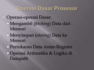
1. Operasi-operasi Dasar:
Mengambil (fetching) Data dari
Memori
Menyimpan (storing) Data ke
Memori
Pertukaran Data Antar-Register
Operasi Aritmatika & Logika di
Datapath
2. Read MFC
Instruksi:
Instruction
LD R2,(R1) ; R2 M[R1] PC
Decoder
Address
lines
MAR IR
Langkah-langkah: Data
lines
1. MAR R1 MDR R1
2. Read Y
3. Tunggu sinyal MFC R2
// MFC = Memory Function Add
Sub
Completed ALU
// Pada saat MFC aktif: XOR
Carry-in
// MDR M[MAR]
Z TEMP
4. R2 MDR
3. Write MFC
Instruksi: PC
Instruction
Decoder
ST (R1),R2 ; M[R1] R2 Address
lines
MAR IR
Data
Langkah-langkah: lines
MDR R1
1. MAR R1 Y
2. MDR R2, Write R2
3. Tunggu sinyal MFC Add
Sub
// MFC = Memory Function ALU
Completed XOR
Carry-in
// Pada saat MFC aktif: Z TEMP
// M[MAR] MDR
4. R1in
Instruksi:
X MOV R4,R1 ; R4 R1
R1
X
R1out Langkah-langkah:
1. Enable output of R1
R4in // setting R1out to 1
X 2. Enable input of R4
R4 // setting R4in to 1
X
R4out
5. Riin
X Instruksi:
Ri ADD R1,R2 ; R1 R1 + R2
X
Riout
Yin Langkah-langkah:
X
Y 1. R1out, Yin
X 2. R2out, Add, Zin
Yout 3. Zout, R1in
A B
ALU
Add X Zin
Z
X
Zout
6. Komponen-komponen Datapath:
Register: tempat penyimpanan data
ALU: tempat pemrosesan aritmatika & logika
Bus: penghubung antar-register & antara register-ALU
Eksekusi Instruksi merupakan kombinasi
pertukaran data antara:
Register Bus Register
Register Bus ALU
Register Bus Memori
Pertukarandata dilakukan dengan cara
mengaktifkan gerbang-gerbang register dengan
menggunakan sinyal-sinyal kendali (PCout, PCin,
dst.)
7.
8. Instruksi:
Add R1,(R3) ; R1 R1 + M[R3]
Langkah-langkah:
1. Fetch instruksi
1. PCout, MARin, Read, Clear Y, Set carry-in to ALU, Add, Zin
2. Zout, PCin, WMFC
3. MDRout, IRin
2. Fetch operand #1 (isi lokasi memori yg ditunjuk oleh
R3)
4. R3out, MARin, Read
5. R1out, Yin, WMFC
3. Lakukan operasi penjumlahan
6. MDRout, Add, Zin
4. Simpan hasil penjumlahan di R1
7. Zout, R1in, End
9. 1. PCout, MARin, Read, Clear Y, Set carry-in to ALU, Add, Zin
2. Zout, PCin, WMFC Control lines
3. MDRout, IRin
Instruction
PC
Decoder
Address
lines
MAR IR
Data
lines
MDR R1
00000000
Y
R3
Add
1
ALU
PC+1 Carry-in
Z TEMP
10. 4. R3out, MARin, Read
5. R1out, Yin, WMFC
Instruction
PC=PC+1
Decoder
Address
lines
MAR IR
Data
lines
MDR R1
Y
R3
ALU
Z TEMP
11. 6. MDRout, Add, Zin
Instruction
PC=PC+1
Decoder
Address
lines
MAR IR
Data
lines
MDR=M[R3] R1
Y=R1
R3
Add
ALU
Carry-in
Zin Z TEMP
12. 7. Zout, R1in, End
Instruction
PC=PC+1
Decoder
Address
lines
MAR IR
Data
lines
MDR=M[R3] R1
Y=R1
R3
ALU
Z=R1+M[R3] TEMP
13. Unconditional (JMP Loop)
1. PCout, MARin, Read, Clear Y, Set carry-in to ALU, Add, Zin
2. Zout, PCin, WMFC
3. MDRout, IRin
4. PCout, Yin
5. Offset-field-of-IRout, Add, Zin // PC PC + Offset
6. Zout, PCin, End
Conditional (contoh: BRNeg Loop)
1. PCout, MARin, Read, Clear Y, Set carry-in to ALU, Add, Zin
2. Zout, PCin, WMFC
3. MDRout, IRin
4. PCout, Yin , If N=0 then End // take the branch?
5. Offset-field-of-IRout, Add, Zin // PC PC + Offset
6. Zout, PCin, End
15. Instruksi:
LD R16,X ; R16 M[X]
Langkah-langkah:
1. Fetch instruksi
1. PCout, MARin, Read, Clear Y, Set carry-in to ALU, Add, Zin
2. Zout, PCin, WMFC
3. MDRout, IRin
2. Fetch operand dari lokasi memori yang ditunjuk oleh
X
4. Xout, MARin, Read
5. WMFC
3. Lakukan operasi ALU
4. Simpan hasil penjumlahan di R16
6. MDRout, R16in, End
16. 1. PCout, MARin, Read, Clear Y, Set carry-in to
Control lines
ALU, Add, Zin
Read
2. Zout, PCin, WMFC
Instruction
3. MDRout, IRin PC
Decoder
4. Xout, MARin, Read Address
lines
PCout
MAR IR
5. WMFC
MARin
6. MDRout, R16in, End Data
lines
MDR X
Clear Y
00000000
Y
R16
Add
1
ALU
Set
PC+1 Carry-in
Z TEMP
Zin
17. 1. PCout, MARin, Read, Clear Y, Set carry-in to
Control lines
ALU, Add, Zin
WMFC
2. Zout, PCin, WMFC
Instruction
3. MDRout, IRin PC
Decoder
4. Xout, MARin, Read Address
lines
PCin
MAR IR
5. WMFC
6. MDRout, R16in, End Data
lines
MDR X
Y
R16
ALU
Z = PC+1 TEMP
Zout
18. 1. PCout, MARin, Read, Clear Y, Set carry-in to
Control lines
ALU, Add, Zin
2. Zout, PCin, WMFC
Instruction
3. MDRout, IRin PC+1
Decoder
4. Xout, MARin, Read Address
lines
MAR IR
5. WMFC
6. MDRout, R16in, End Data
lines
IRin
MDR X
MDRout
Y
R16
ALU
Z TEMP
19. 1. PCout, MARin, Read, Clear Y, Set carry-in to
Control lines
ALU, Add, Zin
Read
2. Zout, PCin, WMFC
Instruction
3. MDRout, IRin PC+1
Decoder
4. Xout, MARin, Read Address
lines
MAR IR
5. WMFC
6. MDRout, R16in, End Data
lines
MARin
MDR X
Xout
Y
R16
ALU
Z TEMP
20. 1. PCout, MARin, Read, Clear Y, Set carry-in to
Control lines
ALU, Add, Zin
WMFC
2. Zout, PCin, WMFC
Instruction
3. MDRout, IRin PC+1
Decoder
4. Xout, MARin, Read Address
lines
MAR IR
5. WMFC
6. MDRout, R16in, End Data
lines
MDR X
Y
R16
ALU
Z TEMP
21. 1. PCout, MARin, Read, Clear Y, Set carry-in to
Control lines
ALU, Add, Zin
2. Zout, PCin, WMFC
Instruction
3. MDRout, IRin PC+1
Decoder
4. Xout, MARin, Read Address
lines
MAR IR
5. WMFC
6. MDRout, R16in, End Data
lines
MDR X
MDRout
Y
R16
R16in
ALU
Z TEMP
23. Instruksi:
ADD R16,R17 ; R16 R16 + R17
Langkah-langkah:
1. Fetch instruksi
1. PCout, MARin, Read, Clear Y, Set carry-in to ALU, Add, Zin
2. Zout, PCin, WMFC
3. MDRout, IRin
2. Fetch operand ke-1 (R16)
4. R16out, Yin
3. Fetch operand ke-2 (R17) dan Lakukan operasi ALU
5. R17out, Add, Zin
4. Simpan hasil penjumlahan di R16
6. Zout, R16in, End
24. 1. PCout, MARin, Read, Clear Y, Set carry-in to
Control lines
ALU, Add, Zin
Read
2. Zout, PCin, WMFC
Instruction
3. MDRout, IRin PC
Decoder
4. R16out, Yin Address
lines
PCout
MAR IR
5. R17out, Add, Zin
MARin
6. Zout, R16in, End Data
lines
MDR R17
Clear Y
00000000
Y
R16
Add
1
ALU
Set
PC+1 Carry-in
Z TEMP
Zin
25. 1. PCout, MARin, Read, Clear Y, Set carry-in to
Control lines
ALU, Add, Zin
WMFC
2. Zout, PCin, WMFC
Instruction
3. MDRout, IRin PC
Decoder
4. R16out, Yin Address
lines
PCin
MAR IR
5. R17out, Add, Zin
6. Zout, R16in, End Data
lines
MDR R17
Y
R16
ALU
Z = PC+1 TEMP
Zout
26. 1. PCout, MARin, Read, Clear Y, Set carry-in to
Control lines
ALU, Add, Zin
2. Zout, PCin, WMFC
Instruction
3. MDRout, IRin PC+1
Decoder
4. R16out, Yin Address
lines
MAR IR
5. R17out, Add, Zin
6. Zout, R16in, End Data
lines
IRin
MDR R17
MDRout
Y
R16
ALU
Z TEMP
27. 1. PCout, MARin, Read, Clear Y, Set carry-in to
Control lines
ALU, Add, Zin
2. Zout, PCin, WMFC
Instruction
3. MDRout, IRin PC+1
Decoder
4. R16out, Yin Address
lines
MAR IR
5. R17out, Add, Zin
6. Zout, R16in, End Data
lines
MDR R17
Yin Y
R16
R16out
ALU
Z TEMP
28. 1. PCout, MARin, Read, Clear Y, Set carry-in to
Control lines
ALU, Add, Zin
2. Zout, PCin, WMFC
Instruction
3. MDRout, IRin PC+1
Decoder
4. R16out, Yin Address
lines
MAR IR
5. R17out, Add, Zin
6. Zout, R16in, End Data
lines
MDR R17
R17out
Y=R16
R16
Add
ALU
Zin Z TEMP
29. 1. PCout, MARin, Read, Clear Y, Set carry-in to
Control lines
ALU, Add, Zin
2. Zout, PCin, WMFC
Instruction
3. MDRout, IRin PC+1
Decoder
4. R16out, Yin Address
lines
MAR IR
5. R17out, Add, Zin
6. Zout, R16in, End Data
lines
MDR R17
Y=R16
R16
R16out
ALU
Zout Z=R16+R17 TEMP