SNOW 3G is a synchronous, word-oriented stream cipher used by the 3GPP standards as a confidentiality and integrity algorithms. It is used as first set in long term evolution (LTE) and as a second set in universal mobile telecommunications system (UMTS) networks. The cipher uses 128-bit key and 128 bit IV to produce 32-bit ciphertext. The paper presents two techniques for performance enhancement. The first technique uses novel CLA architecture to minimize the propagation delay of the 2 modulo adders. The second technique uses novel architecture for S-box to minimize the chip area. The presented work uses VHDL language for coding. The same is implemented on the FPGA device Virtex xc5vfx100e manufactured by Xilinx. The presented architecture achieved a maximum frequency of 254.9 MHz and throughput of 7.2235 Gbps. 32
Design of area optimized aes encryption core using pipelining technologyIAEME Publication
This document summarizes a research paper that proposes a new pipelined design for the AES-128 encryption algorithm to optimize chip area. The design divides the 128-bit plaintext, key, and ciphertext into four 32-bit units and processes them in parallel through 10 pipeline stages, one for each round of encryption. Simulation results show the new design significantly reduces chip pins and area compared to the original iterative design while maintaining encryption speed.
IJRET : International Journal of Research in Engineering and Technology is an international peer reviewed, online journal published by eSAT Publishing House for the enhancement of research in various disciplines of Engineering and Technology. The aim and scope of the journal is to provide an academic medium and an important reference for the advancement and dissemination of research results that support high-level learning, teaching and research in the fields of Engineering and Technology. We bring together Scientists, Academician, Field Engineers, Scholars and Students of related fields of Engineering and Technology
Implementation of a stream cipher based on bernoulli's mapijcsit
A stream cipher was implemented on a FPGA. The keystream, for some authors the most important
element, was developed using an algorithm based on Bernoulli’s chaotic map. When dynamic systems are
digitally implemented, a normal degradation appears and disturbs their behavior; for such reason, a
mechanism was needed. The proposed mechanism gives a solution for degradation issue and its
implementation is not complicated. Finally, the implemented cipher includes 8 stages and 2 pseudo-random
number generators (PRNG), such cipher was tested using NIST testes. Once its designing stage, it was
implemented using a developing FPGA board.
International Journal of Engineering and Science Invention (IJESI) is an international journal intended for professionals and researchers in all fields of computer science and electronics. IJESI publishes research articles and reviews within the whole field Engineering Science and Technology, new teaching methods, assessment, validation and the impact of new technologies and it will continue to provide information on the latest trends and developments in this ever-expanding subject. The publications of papers are selected through double peer reviewed to ensure originality, relevance, and readability. The articles published in our journal can be accessed online.
This paper presents interfaces required in wireless sensor node (WSN) implementation. Here keyboard,
LCD, ADC and Wi-Fi module interfaces are presented. These interfaces are developed as hardware prototypes in
the application of wireless sensor node as a single chip solution. Protocols of these interfaces have been described
with the help of their hardware simulations and synthesis reports.
The end application is proposed to monitor physical parameters remotely using wireless protocol. The sensor node
has to be implemented on Field Programmable Gate Array (FPGA). The proposed node design is reconfigurable,
and hence flexible in context of future modification. Xilinx platform is proposed for synthesis, simulation and
implementation.
Keywords — FPGA, wireless sensor node.
IRJET- A Novel Hybrid Security System for OFDM-PON using Highly Improved RC6 ...IRJET Journal
This document proposes a novel hybrid security system for OFDM-PON using a highly improved RC6 algorithm and scrambling technique. The data is first scrambled using Morlet wavelet transform for spatial domain scrambling without data loss. It is then encrypted using a highly improved RC6 algorithm for enhanced security. By combining scrambling and encryption, a two-tier security approach is implemented with low complexity. Simulation results show low bit and symbol error rates, demonstrating improved system performance. The proposed scheme provides enhanced security for OFDM-PON networks with potential applications in secure optical communications.
International Journal of Computational Engineering Research(IJCER) is an intentional online Journal in English monthly publishing journal. This Journal publish original research work that contributes significantly to further the scientific knowledge in engineering and Technology.
This document proposes a double layer lookup table technique for improving data security when implemented on an FPGA. The technique uses two lookup tables embedded in the FPGA, each with predefined length and contents. Input data is encrypted by XORing it with the values in the first lookup table. This ciphertext is then encrypted again by XORing it with the second lookup table. This makes the real data difficult for an adversary to obtain as they would not know the length or contents of the lookup tables. The design is implemented in FPGA using VHDL programming and synthesis tools to create and download the configuration to the physical device. Experimental results demonstrate the encryption process using example data streams and lookup table values.
The document discusses computer architecture and data manipulation. It describes the central processing unit (CPU) which includes an arithmetic logic unit (ALU) and registers. Data is manipulated by moving values between memory and registers via buses before performing arithmetic operations in the ALU. Programs are stored in memory as machine instructions that the CPU fetches and executes in a series of steps. Later sections cover machine language, program execution, arithmetic instructions, input/output, and parallel processing architectures.
The Advanced Encryption Standard (AES) is a specification for the encryption of electronic data also called Rijndael. The algorithm described by AES is a symmetric-key algorithm, meaning the same key is used for both encrypting and decrypting the data. Hardware-based cryptography is used for authentication of users and of software updates and installations. Software implementations can generally not be used for this, as the cryptographic keys are stored in the PC memory during execution, and are vulnerable to malicious codes. Hardware-based encryption products can also vary in the level of protection they provide against brute force rewind attacks, Offline parallel attacks, or other cryptanalysis attacks. The algorithm was implemented in FPGA due to its flexibility and reconfiguration capability. A reconfigurable device is very convenient for a cryptography algorithm since it allows cheap and quick alterations. The implementation of pipelined cryptography hardware was used to improve performance in order to achieve higher throughput and greater parallelism. The AES hardware was implemented in three modules contains of the encryption, the decryption and the key expansion module.
Implementation of switching controller for the internet routerIAEME Publication
This document summarizes an academic journal article that implements and analyzes a switching controller for an internet router. Specifically:
- The article designs and implements a greedy scheduling algorithm on an FPGA to control the switching of packets between inputs and outputs of a router.
- Two design options for the scheduler are proposed and their performance is analyzed in terms of speed and scalability.
- The implementation is tested and shown to allow scheduling of routers with hundreds of ports within 60 nanoseconds, suitable for high-capacity internet routers.
The document analyzes the performance of the LEON 3FT processor at different operating frequencies. A hardware implementation using the LEON 3FT processor was tested by executing benchmark programs at various frequencies. The results show that execution time decreases with higher operating frequencies, though there is a maximum frequency limit due to hardware constraints. Future work involves attempting to increase this maximum frequency limit while maintaining processor performance.
The document describes the development and testing of a novel mathematical computing architecture called MaPU. Key highlights include a multi-granularity parallel storage system that enables simultaneous matrix row and column access, a high dimension data model, and a cascading pipeline with a state machine-based program model. The first MaPU chip was implemented on a 40nm process with 4 MaPU cores. Testing showed the MaPU core was up to 6.94 times faster than a similar TI C66x DSP core for various algorithms like FFT and matrix multiplication. Power analysis indicated tested power was within 8% of estimated power.
COUPLED FPGA/ASIC IMPLEMENTATION OF ELLIPTIC CURVE CRYPTO-PROCESSORIJNSA Journal
In this paper, we propose an elliptic curve key generation processor over GF(2163) scheme based on the Montgomery scalar multiplication algorithm. The new architecture is performed using polynomial basis. The Finite Field operations use a cellular automata multiplier and Fermat algorithm for inversion. For real time implementation, the architecture has been tested on an ISE 9.1 Software using Xilinx Virtex II Pro FPGA and on an ASIC CMOS 45 nm technology as well. The proposed implementation provides a time of 2.07 ms and 38 percent of Slices in Xilinx Virtex II Pro FPGA. Such features reveal the high efficiently of this implementation design.
The document describes the design and implementation of a Universal Serial Bus (USB) Transceiver Macrocell Interface (UTMI) using Verilog and an FPGA. The UTMI was designed according to USB 2.0 specifications to support data transmission rates up to 480 Mbps. It includes transmitter and receiver modules that handle operations like sync pattern generation/detection, bit stuffing/unstuffing, and NRZI encoding/decoding. The design was simulated and synthesized for an FPGA. The UTMI core can serve as an IP block for USB device controllers and future work may expand it to support higher data rates.
Modification of l3 learning switch code for firewall functionality in pox con...eSAT Journals
The document describes modifications made to the Learning Layer 3 switch code in the POX SDN controller to add basic firewall functionality. A tree network topology with 7 switches and 8 hosts was created using Mininet. The Learning switch code was modified to check for source MAC addresses in packets and only allow communication for pre-defined source MACs by inserting rules in all switches. Testing showed only allowed hosts (h1 to h8) could communicate by matching the rules. The purpose was to provide firewall-like access control over the network using the SDN controller and OpenFlow switches.
The document contains 10 questions related to instrumentation and microprocessor-based systems. Question 1 asks to draw and explain a block diagram of a microprocessor-based instrumentation system and discuss the importance of microprocessors in modern industries. Question 2 asks about the role of the 8255 chip in microprocessor systems and benefits of PCI over ISA. Question 3 defines RS-232 signals and explains simplex and half-duplex connections. The remaining questions cover topics like ADCs, Bluetooth, electrostatic discharge, signal propagation, crosstalk, software development models, process control systems, interfacing, USB, DACs, optical data transmission, reducing noise and interference, high-speed design, trace impedance, software reliability, and
Study on Adaptive PID Control Algorithm Based on RBF Neural NetworkRadita Apriana
Aim at the limitation of traditional PID controller has certain limitation, the traditionalPID control is
often difficult to obtain satisfactory control performance, and the RBF neural networkis difficult to meet the
requirement ofreal-time control system.To overcome it, an adaptive PID control strategy based on (RBF)
neural network isproposed in this paper. The resultsshow that the proposed controller is practical and
effective, because of the adaptability, strong robustness and satisfactory controlperformance.It is also
revealed from simulation results that the proposed control algorithm is valid for DC motor and also
provides the theoretical and experimental basis.
IJRET : International Journal of Research in Engineering and Technology is an international peer reviewed, online journal published by eSAT Publishing House for the enhancement of research in various disciplines of Engineering and Technology. The aim and scope of the journal is to provide an academic medium and an important reference for the advancement and dissemination of research results that support high-level learning, teaching and research in the fields of Engineering and Technology. We bring together Scientists, Academician, Field Engineers, Scholars and Students of related fields of Engineering and Technology.
Transfer of ut information from fpga through ethernet interfaceeSAT Publishing House
IJRET : International Journal of Research in Engineering and Technology is an international peer reviewed, online journal published by eSAT Publishing House for the enhancement of research in various disciplines of Engineering and Technology. The aim and scope of the journal is to provide an academic medium and an important reference for the advancement and dissemination of research results that support high-level learning, teaching and research in the fields of Engineering and Technology. We bring together Scientists, Academician, Field Engineers, Scholars and Students of related fields of Engineering and Technology
Design and implementation of multi channel frame synchronization in fpgaIAEME Publication
This document summarizes a research paper that designed and implemented a multi-channel frame synchronization system in an FPGA. It used low voltage differential signaling receivers to interface satellite data to the FPGA. The FPGA implemented logic for data simulation, frame synchronization, and associated functions like flywheel logic and bit slip correction. Frame synchronization was achieved through correlating received data to a reference pattern, allowing for some bit errors. The design provides reliable synchronization in noisy conditions through an adaptive synchronization strategy and state machine.
The document discusses programmable logic controller instructions for bit shifting, sequencing, and loading. It provides details on:
- Bit shift instructions like bit shift left (BSL) and bit shift right (BSR) that allow basic shift operations on bit arrays
- Sequencer instructions like sequencer output (SQO), sequencer compare (SQC), and sequencer load (SQL) that are useful for outputting, comparing or loading a sequence of data on a recurring basis
- Parameters, status bits, and usage of these instructions including addressing bit arrays, controlling sequence position and length, comparing input to references, and loading data into sequence files.
A New Approach for Video Encryption Based on Modified AES Algorithmiosrjce
IOSR Journal of Computer Engineering (IOSR-JCE) is a double blind peer reviewed International Journal that provides rapid publication (within a month) of articles in all areas of computer engineering and its applications. The journal welcomes publications of high quality papers on theoretical developments and practical applications in computer technology. Original research papers, state-of-the-art reviews, and high quality technical notes are invited for publications.
Implementation of an arithmetic logic using area efficient carry lookahead adderVLSICS Design
An arithmetic logic unit acts as the basic building blocks or cell of a central processing unit of a computer.
And it is a digital circuit comprised of the basic electronics components, which is used to perform various
function of arithmetic and logic and integral operations further the purpose of this work is to propose the
design of an 8-bit ALU which supports 4-bit multiplication. Thus, the functionalities of the ALU in this
study consist of following main functions like addition also subtraction, increment, decrement, AND, OR,
NOT, XOR, NOR also two complement generation Multiplication. And the functions with the adder in the
airthemetic logic unit are implemented using a Carry Look Ahead adder joined by a ripple carry approach.
The design of the following multiplier is achieved using the Booths Algorithm therefore the proposed ALU
can be designed by using verilog or VHDL and can also be designed on Cadence Virtuoso platform.
Customizable Microprocessor design on Nexys 3 Spartan FPGA BoardBharat Biyani
This document describes a customizable microprocessor design created by students at the University of Texas at Dallas. The microprocessor has three main blocks: a keyboard reader for input, a microprocessor unit for processing, and a VGA controller for output display. It implements a RISC architecture with a 16-bit data bus, 12-bit address bus, and 22 instructions. The microprocessor can operate in different modes including programming, execution, and debug modes. It also includes novel features such as real-time register display, flexibility to write to any memory location, and ability to reprogram itself without reloading the bitfile.
This document summarizes an application note for a digital ICT and boundary scan tester. It describes the test setup, which involves connecting portions of a system board containing FPGA chips to the tester via jumper wires. Automatic test pattern generation is used to test for pin-open and pin-short faults on the FPGA chips. Test vectors are generated that check the logic states of the device under test pins and corresponding tester pins. Logging files show the test results with and without an inserted ground fault. The boundary scan cells of the FPGA chips are able to detect the fault locally while the affected tester pin correctly fails the full test.
This document summarizes the implementation of pseudorandom binary sequences (PRBS), specifically maximal length sequences (MLS), for CDMA2000 using MATLAB Simulink. It discusses the properties of MLS, including their use as spreading codes in 2G and 3G standards. The autocorrelation and cross correlation properties of MLS are studied through simulation and verification. Implementation of a 42-stage MLS generator according to the CDMA2000 polynomial is presented.
The document describes a modified radix-24 single-data-path discrete Fourier transform (DFT) algorithm and architecture for implementing a 128-point inverse fast Fourier transform (IFFT) module for use in FPGA-based multiband orthogonal frequency division multiplexing (MB-OFDM) ultra-wideband (UWB) systems. The key aspects of the proposed design include:
1) A modified radix-24 single-data-flow (SDF) DFT algorithm that reorders the twiddle factor sequence to enable easier implementation of complex multiplication compared to earlier designs.
2) A single-data-path pipelined architecture that achieves the required 528 MHz processing speed for the U
International Journal of Engineering Research and Applications (IJERA) is an open access online peer reviewed international journal that publishes research and review articles in the fields of Computer Science, Neural Networks, Electrical Engineering, Software Engineering, Information Technology, Mechanical Engineering, Chemical Engineering, Plastic Engineering, Food Technology, Textile Engineering, Nano Technology & science, Power Electronics, Electronics & Communication Engineering, Computational mathematics, Image processing, Civil Engineering, Structural Engineering, Environmental Engineering, VLSI Testing & Low Power VLSI Design etc.
Hardware implementation of the serpent block cipher using fpga technologyIAEME Publication
This document describes a hardware implementation of the Serpent block cipher using FPGA technology. It provides an overview of the Serpent encryption and decryption algorithms, which operate on 128-bit blocks using a 128, 192, or 256-bit key. The algorithms involve an initial/final permutation, 32 rounds of key mixing, S-box substitutions, and linear transformations. The document also discusses specifics of implementing Serpent on a Xilinx Spartan-6 FPGA, including using the FPGA's look-up tables. Comparisons to other symmetric block ciphers are provided.
Performance Analysis of IEEE 802.15.4 Transceiver System under Adaptive White...IJECEIAES
Zigbee technology has been developed for short range wireless sensor networks and it follows IEEE 802.15.4 standard. For such sensors, several considerations should be taken including; low data rate and less design complexity in order to achieve efficient performance considering to the transceiver systems. This research focuses on implementing a digital transceiver system for Zigbee sensor based on IEEE 802.15.4. The system is implemented using offset quadrature phase shift keying (OQPSK) modulation technique with half sine pulse-shaping method. Direct conversion scheme has been used in the design of Zigbee receiver in order to fulfill the requirements mentioned above. System performance is analyzed considering to BER when it encountered adaptive white Gaussian noise (AWGN), besides showing the effect of using direct sequence spread spectrum (DSSS) technique.
Specifying and Implementing SNOW3G with CryptolUlisses Costa
This document discusses specifying and implementing the SNOW3G stream cipher using the Cryptol domain-specific language. Cryptol allows the algorithm to be specified concisely using its mathematical constructs. The specification must then be refined to meet hardware implementation restrictions in Cryptol. Optimization techniques like converting functions to lookup tables are explored to improve the efficiency of the generated hardware implementation. Preliminary timing and size estimates of the implementation in SPIR format are provided.
Implementation and validation of multiplier less fpga based digital filterIAEME Publication
This document describes an implementation of a finite impulse response (FIR) filter using distributed arithmetic on a field programmable gate array (FPGA). Distributed arithmetic replaces multiplications with lookup tables, reducing complexity. Typically, lookup table size increases exponentially with filter order. The paper proposes using offset binary coding to reduce the lookup table size by a factor of 2 to 2N-1. Simulation results show this implementation requires less FPGA resources than a conventional multiply-accumulate approach.
Design of a unified timing signal generator (utsg) for pulsed radarIAEME Publication
This document describes the design of a Unified Timing Signal Generator (UTSG) for pulsed radar systems. The UTSG is implemented on an FPGA and generates timing signals in four programmable modes to meet various radar timing requirements. It uses a delayed mono-stable pulse generator as the core logic block. The UTSG was tested on a radar controller board where it successfully generated typical radar timing signals like transmit pulses and data windows. Implementation results matched the simulations, demonstrating the UTSG can be used as a flexible timing solution for pulsed radar applications.
International Journal of Engineering Research and Applications (IJERA) is an open access online peer reviewed international journal that publishes research and review articles in the fields of Computer Science, Neural Networks, Electrical Engineering, Software Engineering, Information Technology, Mechanical Engineering, Chemical Engineering, Plastic Engineering, Food Technology, Textile Engineering, Nano Technology & science, Power Electronics, Electronics & Communication Engineering, Computational mathematics, Image processing, Civil Engineering, Structural Engineering, Environmental Engineering, VLSI Testing & Low Power VLSI Design etc.
Embedded processor system for controllable period-width multichannel pulse wi...TELKOMNIKA JOURNAL
This paper proposes a sophisticated embedded processor system configured on zynq-xc7z020 field programmable gate array (FPGA) device for generating four channels pulse width modulation signals with variable duty cycles and periods using embedded design techniques. The main advantages of the technique are the high ability to perform a simultaneous control on period and pulse width of the generated signals and a high system design adaptation to choose the number of input/output channels. Controlling the the period and the pulse width is achieved by injecting a digital signal to the designed system to manipulate embedded timers’ operation. Vivado design suite is used to develop the system hard ware in the integrated development environment where the processing unit and peripherals are instantiated and interconnected. A practical aplication program in C language is prepared to make the system act according to the target. The designed system can be used to drive multi-phase D.C to D.C convertors. The system performance is verified by using vivado logic analyzer and chipscope windows. The superiority of the proposed approach over other approaches is that it resulted in a multi-inputs/multi-outputs pulse width modulation system with high controllability on the pulse width and the period that ranges from 15 nsec to 60 sec.
Implementation of XOR Based Pad Generation Mutual Authentication Protocol for...IOSR Journals
This document describes the implementation of an XOR-based pad generation mutual authentication protocol for RF links. It begins with an introduction to the need for security in RF data transmission and describes existing protocols. It then presents the design of a new XOR pad generation function to securely transmit access passwords for authentication. Random numbers generated by a linear feedback shift register are input to the pad generation function along with passwords to produce encoded pads. The protocol is implemented on an FPGA for hardware verification. Simulation results demonstrate the protocol generating pads for authentication.
Implementation of XOR Based Pad Generation Mutual Authentication Protocol for...IOSR Journals
In RF link, without security the messages exchange between the two devices are monitoring by an
eavesdropper. So the exclusive-OR (XOR) based pad generation protocol is used to safely transfer the data to
the other point with necessary security and it maintaining confidentiality. This protocol produce the cover
coding pad to mask the access password before the datas are transmitted. A specially designed pad generation
will be implemented in digital domain to solve the insecurity problem in data communication RF link. This
protocol developed under regulation of ISO 18000 – 6 type C protocol also known as EPC C1G2 RFID
protocol. The linear feed back shift register (LFSR) generate the pseudo random binary sequence (PRBS) and it
is used as data source to the pad generation function. The Xilinx 13.x software is used for synthesize and
modelsim SE6.0 is used for simulating the result. The pad generation algorithm has been implemented in FPGA
Spartan 3 PQ208-4 board to verify the result
This document describes an FPGA-based design and implementation of an orthogonal frequency division multiplexing (OFDM) transceiver module using VHDL. The key components developed include a serial-to-parallel converter, 4-QAM modulator, 64-point IFFT using a radix-4 butterfly structure, FFT, 4-QAM demodulator, and parallel-to-serial converter. The design utilizes CORDIC algorithms instead of multipliers to improve resource usage. The OFDM transceiver core was implemented and tested on a Xilinx Spartan-3AN FPGA using a loopback configuration.
IRJET-Error Detection and Correction using Turbo CodesIRJET Journal
This document summarizes a research paper on using turbo codes for error detection and correction. It discusses:
1) Turbo codes use parallel convolutional encoders separated by an interleaver to achieve near-Shannon limit performance with forward error correction. The encoding and decoding of text and images is described.
2) Decoding is done iteratively using maximum log-map or log-map algorithms to calculate reliability metrics and soft outputs for error correction.
3) The encoding process involves two recursive systematic convolutional encoders with an interleaver between. Decoding is also iterative and uses log-map type algorithms to calculate branch metrics and state metrics to output soft decisions.
Design and implementation of log domain decoder IJECEIAES
Low-Density-Parity-Check (LDPC) code has become famous in communications systems for error correction, as an advantage of the robust performance in correcting errors and the ability to meet all the requirements of the 5G system. However, the mot challenge faced researchers is the hardware implementation, because of higher complexity and long run-time. In this paper, an efficient and optimum design for log domain decoder has been implemented using Xilinx system generator with FPGA device Kintex7 (XC7K325T-2FFG900C). Results confirm that the proposed decoder gives a Bit Error Rate (BER) very closed to theory calculations which illustrate that this decoder is suitable for next generation demand which needs a high data rate with very low BER.
International Journal of Engineering Research and Applications (IJERA) is an open access online peer reviewed international journal that publishes research and review articles in the fields of Computer Science, Neural Networks, Electrical Engineering, Software Engineering, Information Technology, Mechanical Engineering, Chemical Engineering, Plastic Engineering, Food Technology, Textile Engineering, Nano Technology & science, Power Electronics, Electronics & Communication Engineering, Computational mathematics, Image processing, Civil Engineering, Structural Engineering, Environmental Engineering, VLSI Testing & Low Power VLSI Design etc.
Design and Implementation of an Embedded System for Software Defined RadioIJECEIAES
In this paper, developing high performance software for demanding real-time embed- ded systems is proposed. This software-based design will enable the software engineers and system architects in emerging technology areas like 5G Wireless and Software Defined Networking (SDN) to build their algorithms. An ADSP-21364 floating point SHARC Digital Signal Processor (DSP) running at 333 MHz is adopted as a platform for an embedded system. To evaluate the proposed embedded system, an implementation of frame, symbol and carrier phase synchronization is presented as an application. Its performance is investigated with an on line Quadrature Phase Shift keying (QPSK) receiver. Obtained results show that the designed software is implemented successfully based on the SHARC DSP which can utilized efficiently for such algorithms. In addition, it is proven that the proposed embedded system is pragmatic and capable of dealing with the memory constraints and critical time issue due to a long length interleaved coded data utilized for channel coding.
This document describes the design and implementation of pulse width modulation (PWM) using a hardware/software approach with the MicroBlaze soft-core processor on a Xilinx FPGA. The MicroBlaze processor is programmed in C to generate PWM signals by controlling the clock frequency and adjusting the pulse width without using timer/counter blocks. The PWM design is implemented on a Virtex-5 FPGA and the output signals are displayed on an oscilloscope. The MicroBlaze implementation provides flexibility while using fewer resources and lower power compared to a design using additional memory and timer blocks.
International Journal of Engineering Research and Applications (IJERA) is an open access online peer reviewed international journal that publishes research and review articles in the fields of Computer Science, Neural Networks, Electrical Engineering, Software Engineering, Information Technology, Mechanical Engineering, Chemical Engineering, Plastic Engineering, Food Technology, Textile Engineering, Nano Technology & science, Power Electronics, Electronics & Communication Engineering, Computational mathematics, Image processing, Civil Engineering, Structural Engineering, Environmental Engineering, VLSI Testing & Low Power VLSI Design etc.
Similar to Optimized architecture for SNOW 3G (20)
Redefining brain tumor segmentation: a cutting-edge convolutional neural netw...IJECEIAES
Medical image analysis has witnessed significant advancements with deep learning techniques. In the domain of brain tumor segmentation, the ability to
precisely delineate tumor boundaries from magnetic resonance imaging (MRI)
scans holds profound implications for diagnosis. This study presents an ensemble convolutional neural network (CNN) with transfer learning, integrating
the state-of-the-art Deeplabv3+ architecture with the ResNet18 backbone. The
model is rigorously trained and evaluated, exhibiting remarkable performance
metrics, including an impressive global accuracy of 99.286%, a high-class accuracy of 82.191%, a mean intersection over union (IoU) of 79.900%, a weighted
IoU of 98.620%, and a Boundary F1 (BF) score of 83.303%. Notably, a detailed comparative analysis with existing methods showcases the superiority of
our proposed model. These findings underscore the model’s competence in precise brain tumor localization, underscoring its potential to revolutionize medical
image analysis and enhance healthcare outcomes. This research paves the way
for future exploration and optimization of advanced CNN models in medical
imaging, emphasizing addressing false positives and resource efficiency.
Embedded machine learning-based road conditions and driving behavior monitoringIJECEIAES
Car accident rates have increased in recent years, resulting in losses in human lives, properties, and other financial costs. An embedded machine learning-based system is developed to address this critical issue. The system can monitor road conditions, detect driving patterns, and identify aggressive driving behaviors. The system is based on neural networks trained on a comprehensive dataset of driving events, driving styles, and road conditions. The system effectively detects potential risks and helps mitigate the frequency and impact of accidents. The primary goal is to ensure the safety of drivers and vehicles. Collecting data involved gathering information on three key road events: normal street and normal drive, speed bumps, circular yellow speed bumps, and three aggressive driving actions: sudden start, sudden stop, and sudden entry. The gathered data is processed and analyzed using a machine learning system designed for limited power and memory devices. The developed system resulted in 91.9% accuracy, 93.6% precision, and 92% recall. The achieved inference time on an Arduino Nano 33 BLE Sense with a 32-bit CPU running at 64 MHz is 34 ms and requires 2.6 kB peak RAM and 139.9 kB program flash memory, making it suitable for resource-constrained embedded systems.
Advanced control scheme of doubly fed induction generator for wind turbine us...IJECEIAES
This paper describes a speed control device for generating electrical energy on an electricity network based on the doubly fed induction generator (DFIG) used for wind power conversion systems. At first, a double-fed induction generator model was constructed. A control law is formulated to govern the flow of energy between the stator of a DFIG and the energy network using three types of controllers: proportional integral (PI), sliding mode controller (SMC) and second order sliding mode controller (SOSMC). Their different results in terms of power reference tracking, reaction to unexpected speed fluctuations, sensitivity to perturbations, and resilience against machine parameter alterations are compared. MATLAB/Simulink was used to conduct the simulations for the preceding study. Multiple simulations have shown very satisfying results, and the investigations demonstrate the efficacy and power-enhancing capabilities of the suggested control system.
Neural network optimizer of proportional-integral-differential controller par...IJECEIAES
Wide application of proportional-integral-differential (PID)-regulator in industry requires constant improvement of methods of its parameters adjustment. The paper deals with the issues of optimization of PID-regulator parameters with the use of neural network technology methods. A methodology for choosing the architecture (structure) of neural network optimizer is proposed, which consists in determining the number of layers, the number of neurons in each layer, as well as the form and type of activation function. Algorithms of neural network training based on the application of the method of minimizing the mismatch between the regulated value and the target value are developed. The method of back propagation of gradients is proposed to select the optimal training rate of neurons of the neural network. The neural network optimizer, which is a superstructure of the linear PID controller, allows increasing the regulation accuracy from 0.23 to 0.09, thus reducing the power consumption from 65% to 53%. The results of the conducted experiments allow us to conclude that the created neural superstructure may well become a prototype of an automatic voltage regulator (AVR)-type industrial controller for tuning the parameters of the PID controller.
An improved modulation technique suitable for a three level flying capacitor ...IJECEIAES
This research paper introduces an innovative modulation technique for controlling a 3-level flying capacitor multilevel inverter (FCMLI), aiming to streamline the modulation process in contrast to conventional methods. The proposed
simplified modulation technique paves the way for more straightforward and
efficient control of multilevel inverters, enabling their widespread adoption and
integration into modern power electronic systems. Through the amalgamation of
sinusoidal pulse width modulation (SPWM) with a high-frequency square wave
pulse, this controlling technique attains energy equilibrium across the coupling
capacitor. The modulation scheme incorporates a simplified switching pattern
and a decreased count of voltage references, thereby simplifying the control
algorithm.
A review on features and methods of potential fishing zoneIJECEIAES
This review focuses on the importance of identifying potential fishing zones in seawater for sustainable fishing practices. It explores features like sea surface temperature (SST) and sea surface height (SSH), along with classification methods such as classifiers. The features like SST, SSH, and different classifiers used to classify the data, have been figured out in this review study. This study underscores the importance of examining potential fishing zones using advanced analytical techniques. It thoroughly explores the methodologies employed by researchers, covering both past and current approaches. The examination centers on data characteristics and the application of classification algorithms for classification of potential fishing zones. Furthermore, the prediction of potential fishing zones relies significantly on the effectiveness of classification algorithms. Previous research has assessed the performance of models like support vector machines, naïve Bayes, and artificial neural networks (ANN). In the previous result, the results of support vector machine (SVM) were 97.6% more accurate than naive Bayes's 94.2% to classify test data for fisheries classification. By considering the recent works in this area, several recommendations for future works are presented to further improve the performance of the potential fishing zone models, which is important to the fisheries community.
Electrical signal interference minimization using appropriate core material f...IJECEIAES
As demand for smaller, quicker, and more powerful devices rises, Moore's law is strictly followed. The industry has worked hard to make little devices that boost productivity. The goal is to optimize device density. Scientists are reducing connection delays to improve circuit performance. This helped them understand three-dimensional integrated circuit (3D IC) concepts, which stack active devices and create vertical connections to diminish latency and lower interconnects. Electrical involvement is a big worry with 3D integrates circuits. Researchers have developed and tested through silicon via (TSV) and substrates to decrease electrical wave involvement. This study illustrates a novel noise coupling reduction method using several electrical involvement models. A 22% drop in electrical involvement from wave-carrying to victim TSVs introduces this new paradigm and improves system performance even at higher THz frequencies.
Electric vehicle and photovoltaic advanced roles in enhancing the financial p...IJECEIAES
Climate change's impact on the planet forced the United Nations and governments to promote green energies and electric transportation. The deployments of photovoltaic (PV) and electric vehicle (EV) systems gained stronger momentum due to their numerous advantages over fossil fuel types. The advantages go beyond sustainability to reach financial support and stability. The work in this paper introduces the hybrid system between PV and EV to support industrial and commercial plants. This paper covers the theoretical framework of the proposed hybrid system including the required equation to complete the cost analysis when PV and EV are present. In addition, the proposed design diagram which sets the priorities and requirements of the system is presented. The proposed approach allows setup to advance their power stability, especially during power outages. The presented information supports researchers and plant owners to complete the necessary analysis while promoting the deployment of clean energy. The result of a case study that represents a dairy milk farmer supports the theoretical works and highlights its advanced benefits to existing plants. The short return on investment of the proposed approach supports the paper's novelty approach for the sustainable electrical system. In addition, the proposed system allows for an isolated power setup without the need for a transmission line which enhances the safety of the electrical network
Bibliometric analysis highlighting the role of women in addressing climate ch...IJECEIAES
Fossil fuel consumption increased quickly, contributing to climate change
that is evident in unusual flooding and draughts, and global warming. Over
the past ten years, women's involvement in society has grown dramatically,
and they succeeded in playing a noticeable role in reducing climate change.
A bibliometric analysis of data from the last ten years has been carried out to
examine the role of women in addressing the climate change. The analysis's
findings discussed the relevant to the sustainable development goals (SDGs),
particularly SDG 7 and SDG 13. The results considered contributions made
by women in the various sectors while taking geographic dispersion into
account. The bibliometric analysis delves into topics including women's
leadership in environmental groups, their involvement in policymaking, their
contributions to sustainable development projects, and the influence of
gender diversity on attempts to mitigate climate change. This study's results
highlight how women have influenced policies and actions related to climate
change, point out areas of research deficiency and recommendations on how
to increase role of the women in addressing the climate change and
achieving sustainability. To achieve more successful results, this initiative
aims to highlight the significance of gender equality and encourage
inclusivity in climate change decision-making processes.
Voltage and frequency control of microgrid in presence of micro-turbine inter...IJECEIAES
The active and reactive load changes have a significant impact on voltage
and frequency. In this paper, in order to stabilize the microgrid (MG) against
load variations in islanding mode, the active and reactive power of all
distributed generators (DGs), including energy storage (battery), diesel
generator, and micro-turbine, are controlled. The micro-turbine generator is
connected to MG through a three-phase to three-phase matrix converter, and
the droop control method is applied for controlling the voltage and
frequency of MG. In addition, a method is introduced for voltage and
frequency control of micro-turbines in the transition state from gridconnected mode to islanding mode. A novel switching strategy of the matrix
converter is used for converting the high-frequency output voltage of the
micro-turbine to the grid-side frequency of the utility system. Moreover,
using the switching strategy, the low-order harmonics in the output current
and voltage are not produced, and consequently, the size of the output filter
would be reduced. In fact, the suggested control strategy is load-independent
and has no frequency conversion restrictions. The proposed approach for
voltage and frequency regulation demonstrates exceptional performance and
favorable response across various load alteration scenarios. The suggested
strategy is examined in several scenarios in the MG test systems, and the
simulation results are addressed.
Enhancing battery system identification: nonlinear autoregressive modeling fo...IJECEIAES
Precisely characterizing Li-ion batteries is essential for optimizing their
performance, enhancing safety, and prolonging their lifespan across various
applications, such as electric vehicles and renewable energy systems. This
article introduces an innovative nonlinear methodology for system
identification of a Li-ion battery, employing a nonlinear autoregressive with
exogenous inputs (NARX) model. The proposed approach integrates the
benefits of nonlinear modeling with the adaptability of the NARX structure,
facilitating a more comprehensive representation of the intricate
electrochemical processes within the battery. Experimental data collected
from a Li-ion battery operating under diverse scenarios are employed to
validate the effectiveness of the proposed methodology. The identified
NARX model exhibits superior accuracy in predicting the battery's behavior
compared to traditional linear models. This study underscores the
importance of accounting for nonlinearities in battery modeling, providing
insights into the intricate relationships between state-of-charge, voltage, and
current under dynamic conditions.
Smart grid deployment: from a bibliometric analysis to a surveyIJECEIAES
Smart grids are one of the last decades' innovations in electrical energy.
They bring relevant advantages compared to the traditional grid and
significant interest from the research community. Assessing the field's
evolution is essential to propose guidelines for facing new and future smart
grid challenges. In addition, knowing the main technologies involved in the
deployment of smart grids (SGs) is important to highlight possible
shortcomings that can be mitigated by developing new tools. This paper
contributes to the research trends mentioned above by focusing on two
objectives. First, a bibliometric analysis is presented to give an overview of
the current research level about smart grid deployment. Second, a survey of
the main technological approaches used for smart grid implementation and
their contributions are highlighted. To that effect, we searched the Web of
Science (WoS), and the Scopus databases. We obtained 5,663 documents
from WoS and 7,215 from Scopus on smart grid implementation or
deployment. With the extraction limitation in the Scopus database, 5,872 of
the 7,215 documents were extracted using a multi-step process. These two
datasets have been analyzed using a bibliometric tool called bibliometrix.
The main outputs are presented with some recommendations for future
research.
Use of analytical hierarchy process for selecting and prioritizing islanding ...IJECEIAES
One of the problems that are associated to power systems is islanding
condition, which must be rapidly and properly detected to prevent any
negative consequences on the system's protection, stability, and security.
This paper offers a thorough overview of several islanding detection
strategies, which are divided into two categories: classic approaches,
including local and remote approaches, and modern techniques, including
techniques based on signal processing and computational intelligence.
Additionally, each approach is compared and assessed based on several
factors, including implementation costs, non-detected zones, declining
power quality, and response times using the analytical hierarchy process
(AHP). The multi-criteria decision-making analysis shows that the overall
weight of passive methods (24.7%), active methods (7.8%), hybrid methods
(5.6%), remote methods (14.5%), signal processing-based methods (26.6%),
and computational intelligent-based methods (20.8%) based on the
comparison of all criteria together. Thus, it can be seen from the total weight
that hybrid approaches are the least suitable to be chosen, while signal
processing-based methods are the most appropriate islanding detection
method to be selected and implemented in power system with respect to the
aforementioned factors. Using Expert Choice software, the proposed
hierarchy model is studied and examined.
Enhancing of single-stage grid-connected photovoltaic system using fuzzy logi...IJECEIAES
The power generated by photovoltaic (PV) systems is influenced by
environmental factors. This variability hampers the control and utilization of
solar cells' peak output. In this study, a single-stage grid-connected PV
system is designed to enhance power quality. Our approach employs fuzzy
logic in the direct power control (DPC) of a three-phase voltage source
inverter (VSI), enabling seamless integration of the PV connected to the
grid. Additionally, a fuzzy logic-based maximum power point tracking
(MPPT) controller is adopted, which outperforms traditional methods like
incremental conductance (INC) in enhancing solar cell efficiency and
minimizing the response time. Moreover, the inverter's real-time active and
reactive power is directly managed to achieve a unity power factor (UPF).
The system's performance is assessed through MATLAB/Simulink
implementation, showing marked improvement over conventional methods,
particularly in steady-state and varying weather conditions. For solar
irradiances of 500 and 1,000 W/m2
, the results show that the proposed
method reduces the total harmonic distortion (THD) of the injected current
to the grid by approximately 46% and 38% compared to conventional
methods, respectively. Furthermore, we compare the simulation results with
IEEE standards to evaluate the system's grid compatibility.
Enhancing photovoltaic system maximum power point tracking with fuzzy logic-b...IJECEIAES
Photovoltaic systems have emerged as a promising energy resource that
caters to the future needs of society, owing to their renewable, inexhaustible,
and cost-free nature. The power output of these systems relies on solar cell
radiation and temperature. In order to mitigate the dependence on
atmospheric conditions and enhance power tracking, a conventional
approach has been improved by integrating various methods. To optimize
the generation of electricity from solar systems, the maximum power point
tracking (MPPT) technique is employed. To overcome limitations such as
steady-state voltage oscillations and improve transient response, two
traditional MPPT methods, namely fuzzy logic controller (FLC) and perturb
and observe (P&O), have been modified. This research paper aims to
simulate and validate the step size of the proposed modified P&O and FLC
techniques within the MPPT algorithm using MATLAB/Simulink for
efficient power tracking in photovoltaic systems.
Adaptive synchronous sliding control for a robot manipulator based on neural ...IJECEIAES
Robot manipulators have become important equipment in production lines, medical fields, and transportation. Improving the quality of trajectory tracking for
robot hands is always an attractive topic in the research community. This is a
challenging problem because robot manipulators are complex nonlinear systems
and are often subject to fluctuations in loads and external disturbances. This
article proposes an adaptive synchronous sliding control scheme to improve trajectory tracking performance for a robot manipulator. The proposed controller
ensures that the positions of the joints track the desired trajectory, synchronize
the errors, and significantly reduces chattering. First, the synchronous tracking
errors and synchronous sliding surfaces are presented. Second, the synchronous
tracking error dynamics are determined. Third, a robust adaptive control law is
designed,the unknown components of the model are estimated online by the neural network, and the parameters of the switching elements are selected by fuzzy
logic. The built algorithm ensures that the tracking and approximation errors
are ultimately uniformly bounded (UUB). Finally, the effectiveness of the constructed algorithm is demonstrated through simulation and experimental results.
Simulation and experimental results show that the proposed controller is effective with small synchronous tracking errors, and the chattering phenomenon is
significantly reduced.
Remote field-programmable gate array laboratory for signal acquisition and de...IJECEIAES
A remote laboratory utilizing field-programmable gate array (FPGA) technologies enhances students’ learning experience anywhere and anytime in embedded system design. Existing remote laboratories prioritize hardware access and visual feedback for observing board behavior after programming, neglecting comprehensive debugging tools to resolve errors that require internal signal acquisition. This paper proposes a novel remote embeddedsystem design approach targeting FPGA technologies that are fully interactive via a web-based platform. Our solution provides FPGA board access and debugging capabilities beyond the visual feedback provided by existing remote laboratories. We implemented a lab module that allows users to seamlessly incorporate into their FPGA design. The module minimizes hardware resource utilization while enabling the acquisition of a large number of data samples from the signal during the experiments by adaptively compressing the signal prior to data transmission. The results demonstrate an average compression ratio of 2.90 across three benchmark signals, indicating efficient signal acquisition and effective debugging and analysis. This method allows users to acquire more data samples than conventional methods. The proposed lab allows students to remotely test and debug their designs, bridging the gap between theory and practice in embedded system design.
Detecting and resolving feature envy through automated machine learning and m...IJECEIAES
Efficiently identifying and resolving code smells enhances software project quality. This paper presents a novel solution, utilizing automated machine learning (AutoML) techniques, to detect code smells and apply move method refactoring. By evaluating code metrics before and after refactoring, we assessed its impact on coupling, complexity, and cohesion. Key contributions of this research include a unique dataset for code smell classification and the development of models using AutoGluon for optimal performance. Furthermore, the study identifies the top 20 influential features in classifying feature envy, a well-known code smell, stemming from excessive reliance on external classes. We also explored how move method refactoring addresses feature envy, revealing reduced coupling and complexity, and improved cohesion, ultimately enhancing code quality. In summary, this research offers an empirical, data-driven approach, integrating AutoML and move method refactoring to optimize software project quality. Insights gained shed light on the benefits of refactoring on code quality and the significance of specific features in detecting feature envy. Future research can expand to explore additional refactoring techniques and a broader range of code metrics, advancing software engineering practices and standards.
Smart monitoring technique for solar cell systems using internet of things ba...IJECEIAES
Rapidly and remotely monitoring and receiving the solar cell systems status parameters, solar irradiance, temperature, and humidity, are critical issues in enhancement their efficiency. Hence, in the present article an improved smart prototype of internet of things (IoT) technique based on embedded system through NodeMCU ESP8266 (ESP-12E) was carried out experimentally. Three different regions at Egypt; Luxor, Cairo, and El-Beheira cities were chosen to study their solar irradiance profile, temperature, and humidity by the proposed IoT system. The monitoring data of solar irradiance, temperature, and humidity were live visualized directly by Ubidots through hypertext transfer protocol (HTTP) protocol. The measured solar power radiation in Luxor, Cairo, and El-Beheira ranged between 216-1000, 245-958, and 187-692 W/m 2 respectively during the solar day. The accuracy and rapidity of obtaining monitoring results using the proposed IoT system made it a strong candidate for application in monitoring solar cell systems. On the other hand, the obtained solar power radiation results of the three considered regions strongly candidate Luxor and Cairo as suitable places to build up a solar cells system station rather than El-Beheira.
An efficient security framework for intrusion detection and prevention in int...IJECEIAES
Over the past few years, the internet of things (IoT) has advanced to connect billions of smart devices to improve quality of life. However, anomalies or malicious intrusions pose several security loopholes, leading to performance degradation and threat to data security in IoT operations. Thereby, IoT security systems must keep an eye on and restrict unwanted events from occurring in the IoT network. Recently, various technical solutions based on machine learning (ML) models have been derived towards identifying and restricting unwanted events in IoT. However, most ML-based approaches are prone to miss-classification due to inappropriate feature selection. Additionally, most ML approaches applied to intrusion detection and prevention consider supervised learning, which requires a large amount of labeled data to be trained. Consequently, such complex datasets are impossible to source in a large network like IoT. To address this problem, this proposed study introduces an efficient learning mechanism to strengthen the IoT security aspects. The proposed algorithm incorporates supervised and unsupervised approaches to improve the learning models for intrusion detection and mitigation. Compared with the related works, the experimental outcome shows that the model performs well in a benchmark dataset. It accomplishes an improved detection accuracy of approximately 99.21%.
Introduction- e - waste – definition - sources of e-waste– hazardous substances in e-waste - effects of e-waste on environment and human health- need for e-waste management– e-waste handling rules - waste minimization techniques for managing e-waste – recycling of e-waste - disposal treatment methods of e- waste – mechanism of extraction of precious metal from leaching solution-global Scenario of E-waste – E-waste in India- case studies.
Comparative analysis between traditional aquaponics and reconstructed aquapon...bijceesjournal
The aquaponic system of planting is a method that does not require soil usage. It is a method that only needs water, fish, lava rocks (a substitute for soil), and plants. Aquaponic systems are sustainable and environmentally friendly. Its use not only helps to plant in small spaces but also helps reduce artificial chemical use and minimizes excess water use, as aquaponics consumes 90% less water than soil-based gardening. The study applied a descriptive and experimental design to assess and compare conventional and reconstructed aquaponic methods for reproducing tomatoes. The researchers created an observation checklist to determine the significant factors of the study. The study aims to determine the significant difference between traditional aquaponics and reconstructed aquaponics systems propagating tomatoes in terms of height, weight, girth, and number of fruits. The reconstructed aquaponics system’s higher growth yield results in a much more nourished crop than the traditional aquaponics system. It is superior in its number of fruits, height, weight, and girth measurement. Moreover, the reconstructed aquaponics system is proven to eliminate all the hindrances present in the traditional aquaponics system, which are overcrowding of fish, algae growth, pest problems, contaminated water, and dead fish.
CHINA’S GEO-ECONOMIC OUTREACH IN CENTRAL ASIAN COUNTRIES AND FUTURE PROSPECTjpsjournal1
The rivalry between prominent international actors for dominance over Central Asia's hydrocarbon
reserves and the ancient silk trade route, along with China's diplomatic endeavours in the area, has been
referred to as the "New Great Game." This research centres on the power struggle, considering
geopolitical, geostrategic, and geoeconomic variables. Topics including trade, political hegemony, oil
politics, and conventional and nontraditional security are all explored and explained by the researcher.
Using Mackinder's Heartland, Spykman Rimland, and Hegemonic Stability theories, examines China's role
in Central Asia. This study adheres to the empirical epistemological method and has taken care of
objectivity. This study analyze primary and secondary research documents critically to elaborate role of
china’s geo economic outreach in central Asian countries and its future prospect. China is thriving in trade,
pipeline politics, and winning states, according to this study, thanks to important instruments like the
Shanghai Cooperation Organisation and the Belt and Road Economic Initiative. According to this study,
China is seeing significant success in commerce, pipeline politics, and gaining influence on other
governments. This success may be attributed to the effective utilisation of key tools such as the Shanghai
Cooperation Organisation and the Belt and Road Economic Initiative.
Discover the latest insights on Data Driven Maintenance with our comprehensive webinar presentation. Learn about traditional maintenance challenges, the right approach to utilizing data, and the benefits of adopting a Data Driven Maintenance strategy. Explore real-world examples, industry best practices, and innovative solutions like FMECA and the D3M model. This presentation, led by expert Jules Oudmans, is essential for asset owners looking to optimize their maintenance processes and leverage digital technologies for improved efficiency and performance. Download now to stay ahead in the evolving maintenance landscape.
International Conference on NLP, Artificial Intelligence, Machine Learning an...gerogepatton
International Conference on NLP, Artificial Intelligence, Machine Learning and Applications (NLAIM 2024) offers a premier global platform for exchanging insights and findings in the theory, methodology, and applications of NLP, Artificial Intelligence, Machine Learning, and their applications. The conference seeks substantial contributions across all key domains of NLP, Artificial Intelligence, Machine Learning, and their practical applications, aiming to foster both theoretical advancements and real-world implementations. With a focus on facilitating collaboration between researchers and practitioners from academia and industry, the conference serves as a nexus for sharing the latest developments in the field.
1. International Journal of Electrical and Computer Engineering (IJECE)
Vol. 11, No. 1, February 2021, pp. 545~557
ISSN: 2088-8708, DOI: 10.11591/ijece.v11i1.pp545-557 545
Journal homepage: http://ijece.iaescore.com
Optimized architecture for SNOW 3G
N. B. Hulle1
, Prathiba B2
, Sarika R. Khope3
, K. Anuradha4
, Yogini Borole5
, D. Kotambkar6
1,2,3,5
Department of Electronics and Telecommunication, G H Raisoni Institute of Engineering and Technology, India
4
Department of Computer Science and Engineering, Gokaraju Rangaraju Institute of Engineering and Technology, India
6
Department of Electronics Design Technology, Shri Ramdeobaba College of Engineering and Management, India
Article Info ABSTRACT
Article history:
Received Apr 3, 2020
Revised Jun 19, 2020
Accepted Aug 11, 2020
SNOW 3G is a synchronous, word-oriented stream cipher used by the 3GPP
standards as a confidentiality and integrity algorithms. It is used as first set
in long term evolution (LTE) and as a second set in universal mobile
telecommunications system (UMTS) networks. The cipher uses 128-bit key
and 128 bit IV to produce 32-bit ciphertext. The paper presents two
techniques for performance enhancement. The first technique uses novel
CLA architecture to minimize the propagation delay of the 232
modulo
adders. The second technique uses novel architecture for S-box to minimize
the chip area. The presented work uses VHDL language for coding.
The same is implemented on the FPGA device Virtex xc5vfx100e
manufactured by Xilinx. The presented architecture achieved a maximum
frequency of 254.9 MHz and throughput of 7.2235 Gbps.
Keywords:
Cryptography
FPGA
SNOW 3G
Stream cipher
VHDL
Wireless network security
This is an open access article under the CC BY-SA license.
Corresponding Author:
N. B. Hulle,
Department of Electronics and Telecommunication,
G H Raisoni Institute of Engineering and Technology,
Pune, India.
Email: nagnath.hulle@raisoni.net
1. INTRODUCTION
Security of the records is important in the systems where personal and financial matters are
involved. Hiding of information from unauthorized users becomes essential in such systems and services.
Cryptography is one of the widely used techniques for securing information from eavesdroppers. Considering
the need to secure information many researchers are working in the area of information security. To maintain
advanced network security, the concern network architecture must change from traditional security to
advanced security. The same may be achieved by sinking holes in the security wall.
Cryptography algorithms and their associated key are more secure when it is implemented on
a hardware platform [1]. Side-channel attacks and fault attacks may exist. However, developed algorithms
must be fast enough to support autonomous protocols. These protocols use different encryption algorithms
for a different session. Many recent autonomous protocols like secure sockets layer (SSL) and internet
protocol security (IPsec) use different ciphers for different sessions.
Hardware implementation of the cryptographic algorithm on FPGA devices is attractive solutions
because FPGAs are reconfigurable [2-8]. This property provides flexibility for dynamic system development
and capable of implementing a wide range of functions/architectures/algorithms. It seems to be significant to
emphasize FPGA based implementations of cryptographic algorithms, especially high throughput
architectures [9]. SNOW 3G algorithm is the core of the 3rd generation partnership project (3GPP)
algorithms UEA2 and UIA2. The 3GPP is a joint attempt between telecommunication associations (TG) to
make globally applicable specifications for long term evolution (LTE) mobile phone systems [10, 11].
2. ISSN: 2088-8708
Int J Elec & Comp Eng, Vol. 11, No. 1, February 2021 : 545 - 557
546
The presented work uses optimized architecture for SNOW 3G stream cipher. This architecture
requires only 2K bytes of memory for implementation of S-box in place of 8K bytes of memory required for
the existing SNOW 3G architectures [10-16]. The paper is arranged in the following sections. Section-2
provides initial versions of SNOW stream cipher [17]. Section-3 provides the working and design parameters
of the SNOW 3G algorithm. Section-4 lists existing work related to presented techniques. Section-5 presents
optimized SNOW 3G architecture and its analysis. The results are discussed in Section-6 and Section-7
concludes the presented work.
2. INITIAL VERSIONS OF SNOW
The researcher Patrik Ekdahl et. al. proposed a stream cipher SNOW (SNOW 1.0) in the year
2000 [18], after two years Hawkes et. al. described a new attack known as a guess-and-determine attack [19]
on SNOW 1.0. SNOW 1.0 has two limitations. The first limitation was finite state machine (FSM) has
a single input, which allows the attacker to disturb the working procedure in FSM and second SNOW 1.0 was
little unlucky in choosing feedback polynomial. This allows creating bitwise correspondence in FSM and
which is the base of distinguishing attack.
Patrik Ekdahl et. al. the proposed a new version of SNOW cipher as SNOW 2.0 [20] with
modifications in SNOW 1.0 [18]. They provided two inputs to FSM and modified feedback polynomial in
the new version SNOW 2.0. The two inputs to FSM in SNOW 2.0 makes the guess-and-determine attack
more difficult because FSM update registers R1 and R2 do not depend only on FSM output. The polynomial
selection in SNOW 1.0 was made to speed up the multiplication by left shift operation in LFSR. This allows
the result of multiplication to appear at many places as a bit shifted version of the original word. Such
a selection of polynomial provides a base for correlation attack in the initial version [18]. SNOW 2.0
provides better distribution of the bits in feedback function by defining field (F_2^32) as an extension over
the field (F_2^8). Each multiplication was implemented as shifting the content by one byte and unconditional
XOR with 256 possible patterns. So SNOW 2.0 [20] is strong against correlation attack as compared to Snow
1.0 [18]. During the evaluation of The European Telecommunications Standards Institute (ETSI)/Security
Algorithms Group of Experts (SAGE), the SNOW 2.0 was further modified to increase its resistance against
algebraic attacks and the new design named as SNOW 3G [10].
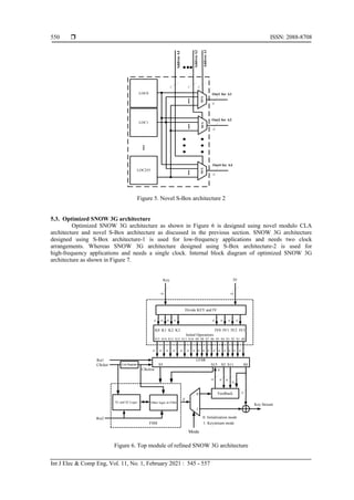
3. SPECIFICATIONS AND WORKING OF SNOW 3G
SNOW 3G generates a 32-bit ciphertext per clock cycle with the help of a 128-bit key and 128-bit
initialization vector (IV) as shown in Figure 1. It consists of the main four modules initial operations,
linear feedback shift register (LFSR), finite state machine (FSM), and a feedback path. The initial operations
will divide 128 bit Key into four blocks as per equations (01), (02), (03), and (04). Similarly, it also divides
128 bit IV into four blocks as per equations (05), (06), (07), and (08) [10].
𝐾3 = 𝑘[0] ‖ 𝑘[1] ‖ 𝑘[2] ‖ … ‖ 𝑘[31] (1)
𝐾2 = 𝑘[32] ‖ 𝑘[33] ‖ 𝑘[34] ‖ … ‖ 𝑘[63] (2)
𝐾1 = 𝑘[64] ‖ 𝑘[65] ‖ 𝑘[66] ‖ … ‖ 𝑘[95] (3)
𝐾0 = 𝑘[96] ‖ 𝑘[97] ‖ 𝑘[98] ‖ … ‖ 𝑘[127] (4)
𝐼𝑉3 = 𝑖𝑣[0] ‖ 𝑖𝑣[1] ‖ 𝑖𝑣[2] ‖ … ‖ 𝑖𝑣[31] (5)
𝐼𝑉2 = 𝑖𝑣[32] ‖ 𝑖𝑣[33] ‖ 𝑖𝑣[34] ‖ … ‖ 𝑖𝑣[63] (6)
𝐼𝑉1 = 𝑖𝑣[64] ‖ 𝑖𝑣[65] ‖ 𝑖𝑣[66] ‖ … ‖ 𝑖𝑣[95] (7)
𝐼𝑉0 = 𝑖𝑣[96] ‖ 𝑖𝑣[97] ‖ 𝑖𝑣[98] ‖ … ‖ 𝑖𝑣[127] (8)
where 𝑘[0], 𝑖𝑣[0] are LSB part and 𝑘[127], 𝑖𝑣[127] are MSB part of the key and IV respectively.
Initial operations are performed on key and iv as per Table 1. The output of the initial operations
block is loaded into LFSR before the first clock cycle [10]. The second module LFSR consists of sixteen
stages each having parallel 32 bits. Contents of LFSR are shifted from MSB (S15) to LSB (S0) in each clock
cycle. S15 receives new value from the feedback path at each clock cycle. Third module FSM consists of
3. Int J Elec & Comp Eng ISSN: 2088-8708
Optimized architecture for SNOW 3G (N. B. Hulle)
547
three parallel 32-bit update registers R1, R2, R3, two S-Boxes S1, S2 each of 4Kbytes, two 32 bit modulo
adders and two 32 bit XOR gates. The final module is the feedback path which consists of functions MULα,
DIVα, and many XOR operations. The two functions MULα and DIVα are implemented as lookup tables.
Divide KEY and IV
128
32 32 32 32 32
K0 K1 K2 K3 IV0 IV1 IV2 IV3
Initial Operations
S15 S14 S13 S12 S11 S10 S9 S8 S7 S6 S5 S4 S3 S2 S1 S0
32
32
32
32 32 32 32 32 32 32 32 32 32 32 32 32 32 32 32
128
LFSR
S5 S15 S2 S11 S0
FSM
32
32
Feedback 32
32
Key Stream
32
32
32
F
v
Key IV
Mode
0
1
0: Initialization mode
1: Keystream mode
Clk
Rst1
Rst2
Figure 1. Existing SNOW 3G architectures
Table 1. LFSR initialization calculations
𝑆0 = 𝐾0 ⊕ 1 𝑆4 = 𝐾0 𝑆8 = 𝐾0 ⊕ 1 𝑆12 = 𝐾0 ⊕ 𝐼𝑉1
𝑆1 = 𝐾1 ⊕ 1 𝑆5 = 𝐾1 𝑆9 = 𝐾1 ⊕ 1 ⊕ 𝐼𝑉3 𝑆13 = 𝐾1
𝑆2 = 𝐾2 ⊕ 1 𝑆6 = 𝐾2 𝑆10 = 𝐾2 ⊕ 1 ⊕ 𝐼𝑉2 𝑆14 = 𝐾2
𝑆3 = 𝐾3 ⊕ 1 𝑆7 = 𝐾3 𝑆11 = 𝐾3 ⊕ 1 𝑆15 = 𝐾3 ⊕ 𝐼𝑉0
SNOW 3G works into two modes of operation, initialization mode and keystream mode. At the start
of initialization, the model system should reset LFSR and FSM using terminals Rst1 and Rst2 respectively.
In the first clock cycle values calculated in the initialization, a mode is loaded into sixteen stages of LFSR but
FSM registers should remain in a reset state. In the second clock cycle, Rst2=0 and now LFSR is clocked.
At each clock, 32-bit output F of FSM is combined with S0, S2 & S11 in the feedback path by selecting
mode 0 from a select line of the multiplexer and applied to S15 as intermediate signal v. The following
equation provides the intermediate signal v in the initialization mode [10].
𝑣 = (𝑆0,1‖𝑆0,2‖𝑆0,3‖0𝑥00) ⊕ 𝑀𝑈𝐿𝛼(𝑆0,0) ⊕ S2 ⊕ (0𝑥00‖𝑆11,0‖𝑆11,1‖𝑆11,2) ⊕
𝐷𝐼𝑉
𝛼(𝑆11,3) ⊕ F (9)
After 32 clock cycles, SNOW 3G enters into keystream mode. Operations in this mode are the same
as initialization mode but the only difference is that output F of FSM is not combined in feedback path by
making mode = 1 from the multiplexer. The intermediate signal in keystream mode is given by the following
equation [10].
𝑣 = (𝑆0,1‖ 𝑆0,2‖𝑆0,3‖0𝑥00) ⊕ 𝑀𝑈𝐿𝛼(𝑆0,0) ⊕ S2 ⊕ (0𝑥00‖𝑆11,0‖𝑆11,1‖𝑆11,2) ⊕
𝐷𝐼𝑉
𝛼(𝑆11,3) (10)
In keystream mode, FSM is clocked for one clock cycle and its first output is discarded when it is clocked for
n clock cycles to encrypt n number of 32-bit words, where n = number of 32-bit data words is to be
encrypted [10].
4. ISSN: 2088-8708
Int J Elec & Comp Eng, Vol. 11, No. 1, February 2021 : 545 - 557
548
4. RELATED WORK
The study of existing architectures of SNOW 3G evolved two challenges. One minimizing
propagation delay of the 232
modulo adders and other is minimizing the chip area of S-boxes. The researcher
Kitsos et al. [12] realized S-boxes using 8 lookup tables. Each lookup table consumes 1 KB memory,
so memory used for S-box realization is 8 KB. Jairaj et al. used symmetry of S-box lookup tables to
minimize cache requirement in the software implementation of SNOW 3G [21]. Kitsos et al. [12] used
conventional CLA for modulo adder implementation. The researcher Pai and Chen [22] presented
a modified CLA design to minimize the propagation delay. Traboulsi et al. [23] implemented SNOW 3G on
an embedded platform. The motive of the design was to minimize the memory required for S-box
implementation. Researchers used 2 lookup tables in place of 8 lookup tables for implementation of
2 S-boxes. Eight-bit shifting with cache memory is used efficiently to minimize memory requirement.
5. PRESENTED SNOW 3G ARCHITECTURE
Considering the challenges of existing FSM, the proposed implementation uses the following
refinements to improve the performance of the SNOW 3G algorithm.
- Use of novel modulo CLA architecture over 232
to minimize propagation delay in FSM, which decides
the critical delay of the algorithm
- Use of novel S-Box architecture to minimize chip area
5.1. Novel modulo CLA architecture over 232
Modulo adders are usually implemented by using ripple-carry adders, but this technique increases
the propagation delay of the critical path. The propagation delay of n bit ripple carries adder is (2n+1) gate
delays. Modulo adder over 232
implemented by using ripple-carry adders will have delay of
(2*32+1 = 65) 65 gates delay, assuming average gate delay of 10 ηs the total delay of one modulo adder will
be 65*10 = 650 ηs. FSM consists of two such adders so a total delay of modulo adders for single
computation will be 1300 ηs.
The propagation delay of modulo adders can be minimized by using CLA for its implementation.
Existing CLAs are realized by using basic gates i.e. AND, XOR, and OR gates, but Pai et al. realized CLA
by using universal gates i.e. NAND or NOR gates [22]. The same design minimized gate requirement as
compared to existing architectures. At the same time, this CLA [22, 24] designs are faster than conventional
CLA architectures. Adder architecture [25] developed for LILI-II cipher uses different approach for
addiation.
Reduction in propagation delay and chip area is possible in existing architectures [12-16, 22],
so the presented research work uses universal gates for CLA implementation and other techniques to
minimize the number of gates required. Novel modulo CLA architecture over 232
uses following three
architectures in multilevel CLA designs for performance improvement
- 4 bit CLA at LSB (to calculate S0 to S3)
- 4 bit CLA at middle stages (to calculate S4 to S27)
- 4 bit CLA at MSB (to calculate S28 to S31)
Using the above CLA architectures novel architecture for modulo CLA over 232
was designed as
shown in Figure 2. Presented modulo adder architecture is an area, propagation delay, and energy-efficient as
compared to existing modulo CLA architectures.
Gate reduction at level 2, Stage 1
Unused
logic circuit
reduction
Four bit LSB
adder
Four bit middle stage adder
Four bit MSB
adder
Gate reduction at level 3, stage 1
FA_WC
S0 G0
B0 A0
FA_NAND
S1 G1 P1
B1 A1
C1
FA_NAND
S2 G2 P2
B2 A2
C2
FA_NAND
S3 G3 P3
B3 A3
C3
GG0
FA_NAND
S4
G4 P4
B4 A4
C4
FA_NAND
S5
G5 P5
B5 A5
C5
FA_NAND
S6
G6 P6
B6 A6
C6
FA_NAND
S7
G7 P7
B7 A7
C7
GG1 PG1
N1
N3
N6
N13
N12
N11
N10
N14
N2
N4
N5
N8
N7
N9
FA_NAND
S8
G8 P8
B8 A8
C8
FA_NAND
S9
G9 P9
B9 A9
C9
FA_NAND
S10
G10 P10
B10 A10
C10
FA_NAND
S11
G11 P11
B11 A11
C11
GG2 PG2
N1
N3
N6
N13
N12
N11
N10
N14
N2
N4
N5
N8
N7
N9
FA_NAND
S12
G12P12
B12 A12
C12
FA_NAND
S13
G13P13
B13 A13
C13
FA_NAND
S14
G14 P14
B14 A14
C14
FA_NAND
S15
G15 P15
B15 A15
C15
GG3
N1
N3
N6
N13
N12
N11
N10
N14
N2
N4
N5
N8
N7
N9
PG3
GG16
FA_NAND
S16
G16P16
B16 A16
FA_NAND
S17
G17P17
B17 A17
C17
FA_NAND
S18
G18 P18
B18 A18
C18
FA_NAND
S19
G19 P19
B19 A19
C19
GG4
N1
N3
N6
N13
N12
N11
N10
N14
N2
N4
N5
N8
N7
N9
PG4
FA_NAND
S20
G20P20
B20 A20
FA_NAND
S21
G21P21
B21 A21
C21
FA_NAND
S22
G22 P22
B22 A22
C22
FA_NAND
S23
G23 P23
B23 A23
C23
GG5
N1
N3
N6
N13
N12
N11
N10
N14
N2
N4
N5
N8
N7
N9
PG5
FA_NAND
S24
G24P24
B24 A24
FA_NAND
S25
G25P25
B25 A25
C25
FA_NAND
S26
G26 P26
B26 A26
C26
FA_NAND
S27
G27 P27
B27 A27
C27
GG6
N1
N3
N6
N13
N12
N11
N10
N14
N2
N4
N5
N8
N7
N9
PG6
C16
C20
C24
FA_NAND
S28 G28 P28
B28 A28
FA_NAND
S29 G29 P29
B29 A29
C29
FA_NAND
S30 G30 P30
B30 A30
C30
FA_NAND_WGIPI
S31
B31 A31
C31 C28
Figure 2. Novel modulo CLA architecture over 232
5. Int J Elec & Comp Eng ISSN: 2088-8708
Optimized architecture for SNOW 3G (N. B. Hulle)
549
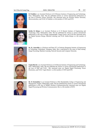
5.2. Novel S-Box architecture
Two S-boxes S1 & S2 are used in SNOW 3G architecture each requires memory of 4 KB.
The lookup table of S1 is taken from the Rijndael substitution box and a lookup table of S2 is based on
Dickson polynomial over GF-28. As per design specification, each S-box (S1 or S2) is implemented by using
4 lookup tables and each lookup table has 256 values each of 4 bytes. So the implementation of each lookup
table requires (256x4 = 1024bytes of memory). Each S-box has 4 lookup tables, so total memory required for
the implementation of S1 or S2 is (4x1024 = 4K) 4KB. The total memory needed for the realization of two
S-boxes is 8KB. Existing implementation [10-16, 26-29] uses S-box architecture as shown in Figure 3.
S1_T0
S1_T1
S1_T2
S1_T3
32
8
8
8
8
32
32
32
32
32
S2_T0
S2_T1
S2_T2
S2_T3
32
8
8
8
8
32
32
32
32
32
S-box S1 Implementation S-box S2 Implementation
Figure 3. Existing S-boxes architecture
The four lookup tables of S1 i.e. S1_T0 to S1_T3 as shown in Figure 3 has the same content but
exist in 8 bit shifted form. Analogous is the case of S-box S2. Presented novel S-box architectures use
a single lookup table for implementation of S-box (S1 or S2). Presented research work uses two architectures
for S-box implementation. First architecture as shown in Figure 4, consumes fewer resources but useful to
low-frequency applications only. Second architecture as shown in Figure 5, consumes fewer resources as
compared to existing architectures but required more resources as compared to Novel S-box architecture-1.
Addr1
Addr2
Addr3
Addr4
DataOut1
DataOut2
DataOut3
DataOut4
8
8
8
8
32
32
32
32
Multiport
ROM
8
32
32 Bit
Latch
32
32
32
32
32 Bit
Latch
32 Bit
Latch
32 Bit
Latch
2 Bit
Counter
Figure 4. Novel S-Box architecture1
Presented designs require 2 KB of memory for the realization of S-boxes S1 & S2. These designs
save 6 KB of memory as compared to existing designs. S-box architecture-1 saves 6 KB memory at the cost
of some additional hardware (Single 2-bit counter, two 4 I/p multiplexers, and four 32 bit latches).
This architecture is 4 times slower than conventional architectures and useful for low-frequency applications.
S-box architecture-2 has the same speed as conventional architectures but uses 4 additional
256:1 multiplexers. The second architecture can be used for low and high-speed applications depending on
cost and speed tradeoffs
6. ISSN: 2088-8708
Int J Elec & Comp Eng, Vol. 11, No. 1, February 2021 : 545 - 557
550
LOC1
LOC0
LOC255
MUX
MUX
MUX
Out1 for A1
Out2 for A2
Out4 for A4
Address
A1
Address
A2
Address
A4
32
32
32
8 8 8
Figure 5. Novel S-Box architecture 2
5.3. Optimized SNOW 3G architecture
Optimized SNOW 3G architecture as shown in Figure 6 is designed using novel modulo CLA
architecture and novel S-Box architecture as discussed in the previous section. SNOW 3G architecture
designed using S-Box architecture-1 is used for low-frequency applications and needs two clock
arrangements. Whereas SNOW 3G architecture designed using S-Box architecture-2 is used for
high-frequency applications and needs a single clock. Internal block diagram of optimized SNOW 3G
architecture as shown in Figure 7.
Divide KEY and IV
128
32 32 32 32 32
K0 K1 K2 K3 IV0 IV1 IV2 IV3
Initial Operations
S15 S14 S13 S12 S11 S10 S9 S8 S7 S6 S5 S4 S3 S2 S1 S0
32
32
32
32 32 32 32 32 32 32 32 32 32 32 32 32 32 32 32
128
LFSR
S5 S15 S2 S11 S0
Feedback 32
32
Key Stream
32
32
32
F
v
Key IV
Mode
0
1
0: Initialization mode
1: Keystream mode
Clkfast
Rst1
S1 and S2 Logic
2 bit Register
Clkslow
Other logic in FSM
Rst2
FSM
Figure 6. Top module of refined SNOW 3G architecture
7. Int J Elec & Comp Eng ISSN: 2088-8708
Optimized architecture for SNOW 3G (N. B. Hulle)
551
32
32 32
S0
S1
S2
S5
S14
S15 ..
..
..
LFSR
32
R3
R1 S2-BOX
R2
S1-BOX
32
32
32
32
32 32
32
32
32
Feedback
FSM
Mode
0
1
32
S11
Divide KEY and IV
128
K0 K1 K2 K3 IV0 IV1 IV2 IV3
Initial Operations
S15 S14 S13 S12 S11 S10 S9 S8 S7 S6 S5 S4 S3 S2 S1 S0
128
KEY IV
Key Stream
Out
32
32
32
32
32
32
32 32
32
32 32
32
32
32
32 32
32 32 32 32 32 32
32 32
32
DIVα
>> 8
32
32
32
32
MULα
<< 8
32
0: Initialization mode
1: Keystream mode
0
1
F
v
Mod CLA
Mod CLA
Figure 7. Internal block diagram of optimized SNOW 3G architecture
FSM of SNOW 3G architecture consists of two modulo adders and two S-Boxes. Two modulo
adders will decide the speed of the algorithm and two S-boxes will decide hardware utilization of
the algorithm. The use of novel modulo CLA over 232
minimizes propagation delay and the use of novel
S-box architecture minimizes hardware utilization. These refinements help to improve the performance of
the SNOW 3G algorithm in terms of throughput and area.
Optimized SNOW 3G architecture uses VHDL language for coding. The same is implemented on
the FPGA device Virtex xc5vfx100e manufactured by Xilinx [30]. The presented architecture achieved
a maximum frequency of 254.9 MHz and throughput of 7.2235 Gbps. Table 2 shows particulars about
the technology used. Figure 8 and Figure 9 show RTL schematic and output waveform of the presented
architecture respectively.
Table 2. Technology used details
SNOW3GNEW Project Status (05/03/2020 - 11:34:41)
Project File: SNOW3GOPT.xise Parser Errors: No Errors
Module Name: SNOW3G Implementation State: Synthesized
Target Device: xc5vfx100t-3ff1136 Errors: No Errors
Product Version: ISE 13.2 Warnings: No Warnings
Design Goal: Balanced Routing Results:
Design Strategy: Xilinx Default (unlocked) Timing Constraints:
Environment: System Settings Final Timing Score:
8. ISSN: 2088-8708
Int J Elec & Comp Eng, Vol. 11, No. 1, February 2021 : 545 - 557
552
Figure 8. RTL schematic
Figure 9. Output waveform
6. RESULT AND DISCUSSIONS
The following section discusses the result in terms of area, propagation delay, throughput,
and memory utilized for presented SNOW 3G architecture.
6.1. The area
6.1.1. Novel modulo CLA architecture over 232
Presented novel modulo CLAs are used as modulo adders over 232
in Optimized SNOW 3G
architecture. A comparison of device utilization of existing [13, 22] and presented architectures is shown
in Figure 10.
9. Int J Elec & Comp Eng ISSN: 2088-8708
Optimized architecture for SNOW 3G (N. B. Hulle)
553
Figure 10. Comparisons of hardware utilization for CLA architectures
6.1.2. Novel S-Box architecture
Optimized SNOW 3G architecture uses Novel S-box architecture to avoid redundancy of lookup
tables. Presented Novel S-Box architecture-1 is suitable for low-frequency applications and Novel S-Box
architecture-2 is useful for high-frequency applications. The use of these novel architectures minimizes
hardware requirement as shown in the Figure 11. The comparison shows that the hardware resources used in
the presented architectures are less than existing architectures [12-16]. The reduction in area is possible
because S-box is designed using one lookup table in place of four lookup tables.
Figure 11. Comparisons of hardware utilization for S-box
6.1.3. Optimized SNOW 3G architecture
Optimized SNOW 3G architecture uses refined modulo CLA over 232
and refined S-box to for
performance improvement. Hardware resources used by optimized SNOW 3G architecture are presented in
Table 3 and Table 4 shows comparisons of hardware resources used by optimized SNOW 3G and existing
architectures [12-16].
The comparison shows that optimized SNOW 3G architecture utilizes minimum resources as
compared to architecture presented Kitsos et al. [13], Madani and anougast [15] and Madani et al. [16].
The architecture presented by Kitsos et al. [12] is ASIC, so the comparison is difficult. The architecture
presented by Zhang et al. [14] uses less hardware as compared to proposed refined architecture because only
one mode implemented on hardware.
94
52 55
102
57 57
103
57 55
0
20
40
60
80
100
120
4 input LUTs Occupied Slices Slices containing Related Logic
Presented Novel Modulo CLA Exisisting Conventional CLA [13] Exisisting Modified CLA [22]
534
1152
2048
748
2304
4164
0
500
1000
1500
2000
2500
3000
3500
4000
4500
Proposed Low Frequency
Architecture
Proposed High frequency
Architecture
Existing Architectures [12, 13, 14,
15, 16]
No. of slices used Number of 4 input LUTs
10. ISSN: 2088-8708
Int J Elec & Comp Eng, Vol. 11, No. 1, February 2021 : 545 - 557
554
Table 3. Device utilization summary of optimized SNOW 3G architecture
Device Utilization Summary (estimated values)
Logic Utilization Used Available Utilization
1. Number of Slice Registers 870 64000 1%
2. Number of Slice LUTs 1208 64000 1%
3. Number of fully used LUT-FF pairs 680 1398 48%
4. Number of bonded IOBs 325 640 50%
5. Number of BUFG/BUFGCTRLs 10 32 31%
Table 4. Comparison of hardware resources for different architectures
Sr. No. Architectures Hardware resources used
1 Proposed Refined Architecture 870 Slice Registers and 1208 slice LUTs on Virtex 5
2 The architecture proposed by P. Kitsos et al. [12] ASIC implementation used 25016 equivalent gates
3 The architecture proposed by P. Kitsos et al. [13] Slices used 3559 on Spartan 3 Family
4 The architecture proposed by L. Zhang et al. [14]
Only one mode implemented on hardware to increase throughput
with minimum hardware resources, 356 slices on Virtex 5
5
The architecture proposed by Mahdi Madani and Camel
Tanougast [15]
1020 Slice Registers and 889 Slice LUTs on Virtex5
6
The architecture proposed Mahdi Madani, Ilyas
Benkhaddra et al. [16]
912 Slice Registers and 1108 Slice LUTs on Virtex 5
6.2. Propagation delay
6.2.1. Novel modulo CLA over 232
Propagation delay comparison of proposed refined CLA and existing CLA architectures [13, 22] is
shown in Figure 12. Propagation delay evaluation shows that delay of presented novel modulo CLA
architecture is fewer than existing CLA architectures. The presented CLA architecture will help to improve
the throughput of Optimized SNOW 3G architecture.
Figure 12. Delay comparisons of novel and existing CLA architectures
6.2.2. Novel S-Box architecture
The combinational path delay comparisons of proposed refined S-box architectures and existing
S-box architectures [12-16] are shown in the Table 5. The comparison shows that the propagation delay of
proposed low-frequency architecture is more as compared to other architectures, with less hardware.
Similarly, the propagation delay of proposed high-frequency architecture is less as compared to other
architectures with moderate hardware utilization. The path delay of existing architectures is more as
compared to presented architecture 1 but less as compared to architecture 2. The hardware resources used by
existing architecture are more as compared to other architectures.
11. Int J Elec & Comp Eng ISSN: 2088-8708
Optimized architecture for SNOW 3G (N. B. Hulle)
555
Table 5. Hardware used and propagation delay comparison of S-box implementations
Sr. No. S- Box architectures
No. of slices
used
Number of 4
input LUTs
Propagation
delay (ns)
1 Proposed Low-Frequency Architecture 534 748 9.92
2 Proposed High-frequency Architecture 1152 2304 9.12
3 Existing Architecture 2048 4164 9.34
6.3. Throughput and memory
Comparisons of throughput achieved and memory used for S-box realization of optimized SNOW
3G and existing SNOW 3G [12-16] architectures are shown in Figure 13. The comparison shows that
throughput of optimized SNOW 3G is higher than architecture presented by Kitsos et al. [13], close to
architecture presented by Kitsos et al. [12], but less than architecture presented by Zhang et al. [14], Madani
and Tanougast [15] and Madani et al. [16]. This may be due to the use of more hardware resources.
Figure 13. Comparisons throughput and memory used for the realization of S-boxes
7. CONCLUSION
Optimized SNOW 3G architecture is presented in the paper uses novel modulo CLA and novel
S-box architecture. The use of novel CLA minimizes hardware required for modulo adders and minimizes
propagation delay as compared to existing architectures. The use of novel S-box architecture minimizes 6 K
bytes of memory as compared to existing architectures. The presented architecture uses 2K bytes of memory,
whereas existing architectures 8 K bytes of memory for the same. The presented SNOW architecture attained
throughput of 7.2463 Gbps at a clock frequency of 226.562 MHz. Presented architecture achieves throughput
more than architecture and close to ASIC implementation.
The throughput of existing architectures is more than the presented architecture. It may be due to:
(1) S-boxes used in these architectures use 8 KB memory for S-box realizations; (2) Architecture uses
a software platform that helps to minimize hardware and to increase throughput; (3) Architecture is ASIC
realization and ASIC designs are always faster than FPGA realizations.
REFERENCES
[1] C. Y. Yan and R. Xiao, “Study of block algorithms implement on hardware in an information security system,”
in Business Management and Electronic Information (BMEI), pp. 589-593, 2011.
[2] P. Leglise, et al., “Efficient Implementation of Recent Stream Ciphers on Reconfigurable Hardware Devices,”
in 26th Symposium on Information Theory in the Benelux, pp. 261-268, 2005.
[3] B. Prathiba, et al., “FPGA Implementation of Smart Cryptography Algorithm,” in International Journal of Recent
Technology and Engineering (IJRTE), vol. 8, no. 5, pp. 3017-3020, 2020.
[4] B. Wang and L. Liu, “A flexible and energy-efficient reconfigurable architecture for symmetric cipher processing,”
in IEEE International Symposium on Circuits and Systems, vol. 14, pp. 1182-1185, 2015.
[5] Y. Chen, et al., “Research and Implementation of Reconfigurable Architectures of DES and ZUC,” in Second
Advanced Information Technology, Electronic and Automation Control Conference (IAEAC), vol. 7, no. 1,
pp. 216-220, 2017.
12. ISSN: 2088-8708
Int J Elec & Comp Eng, Vol. 11, No. 1, February 2021 : 545 - 557
556
[6] N. B. Hulle, et al., “Compact Reconfigurable Architecture for Sosemanuk Stream Cipher,” in International Journal
of Engineering and Advanced Technology (IJEAT), vol. 9, no. 3, pp. 607-611, 2020.
[7] A. Khalid, et al., “RC4-AccSuite: A Hardware Acceleration Suite for RC4-Like Stream Ciphers,” IEEE
Transactions on Very Large Scale Integration (VLSI) Systems, vol. 25, no. 3, pp. 1072-1084, 2017.
[8] G. Paul and A. Chattopadhyay, “Three Snakes in One Hole : A 67 Gbps Flexible Hardware for SOSEMANUK with
Optional Serpent and SNOW 2.0 Modes,” in IACR Cryptology ePrint Archive, pp. 1-19, 2013.
[9] M. Galanis, et al., “Comparison of the Hardware Implementation of Stream Ciphers,” The International Arab
Journal of Information Technology, vol. 2, no. 4, pp. 267-274, 2005.
[10] “Specification of the 3GPP Confidentiality and Integrity Algorithms UEA2 & UIA2, Document 2: SNOW 3G
specification,” ETSI/SAGE Specification, Version 1.1, 2006.
[11] “Specification of the 3GPP Confidentiality and Integrity Algorithms UEA2 & UIA2, Document 3: Implementor’s
Test Data,” ETSI/SAGE Specification, Version 1.1, 2012.
[12] P. Kitsos, et al., “High-Performance ASIC Implementation of the SNOW 3G Stream Cipher,” in IFIP/IEEE VLSI-
SOC 2008 - International Conference on Very Large Scale Integration (VLSI SOC), Rhodes Island, Greece,
pp. 1-4, 2008.
[13] P. Kitsos, et al., “FPGA-based performance analysis of stream ciphers ZUC, Snow3g, Grain V1, Mickey V2,
Trivium and E0,” Microprocessors and Microsystems, vol. 37, no. 2, pp. 235-245, 2013.
[14] L. Zhang, et al., “Evaluating the Optimized Implementations of SNOW 3G and ZUC on FPGA,” in Trust, Security
and Privacy in Computing and Communications (TrustCom), pp. 436-442, 2012.
[15] M. Madani and C. Tanougast, “Combined and Robust SNOW-ZUC Algorithm Based on Chaotic System,” in 2018
International Conference on Cyber Security and Protection of Digital Services, Cyber Security, pp. 1-7, 2018.
[16] M. Madani, et al., “Digital Implementation of an Improved LTE Stream Cipher Snow-3G Based on Hyperchaotic
PRNG,” Security and Communication Networks, vol. 2017, no. 2, pp. 1-15, 2017.
[17] R. D. Kharadkar and N. B. Hulle, “FPGA Implementation of Modulo (231
-1) Adder,” in 7th
International
Conference on Emerging Trends in Engineering & Technology, Kobe, Japan, pp. 85 -90, 2015.
[18] P. Ekdahl and T. Johansson, “SNOW - a new stream cipher,” in RST open Nessie workshop, Heverlee, Belgium,
pp. 1-17, 2001.
[19] P. Hawkes and G. G. Rose, “Guess-and-Determine Attacks on SNOW,” in SAC 2002 Revised Papers from the 9th
Annual International Workshop on Selected Areas in Cryptography, pp. 37-46, 2002.
[20] P. Ekdahl and T. Johansson, “A New Version of the Stream Cipher SNOW,” in International Workshop on
Selected Areas in Cryptography, pp. 47-61, 2002.
[21] V. Jairaj, et al., “High Performance Implementation of Snow3G Algorithm in Memory Limited Environments,”
in New Technologies, Mobility, and Security (NTMS), no. 5, pp. 1-4, 2011.
[22] Y. Pai and Y. Chen, “The Fastest Carry Lookahead Adder,” in Second IEEE International Workshop on Electronic
Design, Test and Applications, no. 1, pp. 4-6, 2004.
[23] S. Traboulsi, et al., “An Optimized Parallel and Energy-Efficient Implementation of SNOW 3G for LTE Mobile
Devices,” in International Conference on Communication Technology (ICCT), pp. 535-538, 2010.
[24] N. B. Hulle, et al., “The Novel Architecture for Carry Lookahead Adder,” Technical Journal of The Institution of
Engineers (India), Pune Local Centre, vol. 36, no. 1, pp. 84-88, 2012.
[25] N. B. Hulle, et al., “High Performance Architecture for LILI-II Stream Cipher,” in International Journal of
Computer Applications, vol. 107, no. 13, pp. 10-13, 2014.
[26] G. Orhanou, et al., “SNOW 3G Stream Cipher Operation and Complexity Study,” Contemporary Engineering
Sciences, vol. 3, no. 3, pp. 97-111, 2010.
[27] S. Hessel, et al., “Implementation and Benchmarking of Hardware Accelerators for Ciphering in LTE Terminals,”
in Global Telecommunications Conference, pp. 1-7, 2009.
[28] N. P. Maity and R. Maity, “Design and Modelling of Paralleled RAM Architecture,” in International Conference
on Future Information Technology, vol. 13, pp. 98-102, 2011.
[29] A. Bikos and N. Sklavos, “Architecture Design of an Area Efficient High-Speed Crypto Processor for 4G LTE,”
IEEE Transactions on Dependable and Secure Computing, vol. 15, no. 5, pp. 729-741, 2018.
[30] xilinx.com, “XUPV5-LX110T,” 2015. [Online], Available: http://www.xilinx.com/univ/xupv5-lx110t.htm.
BIOGRAPHIES OF AUTHORS
Dr. N. B. Hulle is an Associate Professor at G H Raisoni Institute of Engineering and
Technology, Pune, Maharashtra, India. He completed his Bachelor's and Masters from Dr.
Babasaheb Ambedkar Marathwada University, Aurangabad, Maharashtra, India, and Ph.D. from
Rashtrasant Tukadoji Maharaj Nagpur University, Nagpur, Maharashtra, India. He has 21 years
of teaching experience. He guides UG and PG students. His area of research is VLSI,
cryptography & Wireless Network Security. He published papers in National & International
Journals and conferences. Dr. N. B. Hulle is a life member of ISTE and IETE.
13. Int J Elec & Comp Eng ISSN: 2088-8708
Optimized architecture for SNOW 3G (N. B. Hulle)
557
B. Prathiba is an Assistant Professor at G H Raisoni Institute of Engineering and Technology,
Pune, Maharashtra, India. She has published articles in various international publications in
the area of Wireless Sensor Networks. Her interested areas are Wireless Sensor Networks,
Microcontrollers, and VLSI. B. Prathiba is a life member of ISTE and IETE.
Sarika R. Khope is an Assistant Professor at G H Raisoni Institute of Engineering and
Technology, Pune, Maharashtra, India. She has published the articles in various international
publications in the area of Image steganography, Image Fusion, and VLSI Her interested areas
are Digital Systems Design, Machine Learning, and VLSI. Sarika Khope is a life member of
ISTE.
Dr. K. Anuradha is a Professor and Dean ICT at Gokaraju Rangaraju Institute of Engineering
& Technology, Hyderabad, Telangana, India. She is specialized in the areas of Data mining,
Image Processing, Machine Learning, Network Security and Computer Networks.
Yogini Borole is an Assistant Professor at G H Raisoni Institute of Engineering and Technology,
Pune, Maharashtra, India. She has published the articles in various international publications in
the area of DSP and VLSI. Her interested areas are Digital Signal Processing, Power
Electronics, and VLSI. Yogini Borole is a life member of ISTE and IETE.
Dr. D. Kotambkar is an Assistant Professor at Shri Ramdeobaba College of Engineering and
Management, Nagpur, Maharashtra, India. She has published the articles in various international
publications in the area of MIMO Wireless Communication.Her interested areas are Digital
Signal Processing and Wireless Communication..She is a life member of IETE.