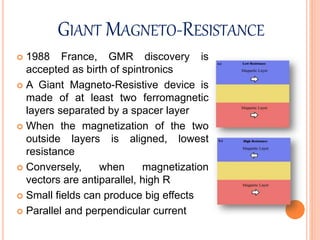
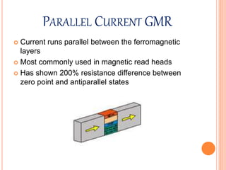
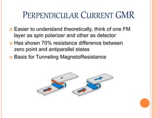
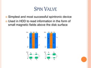
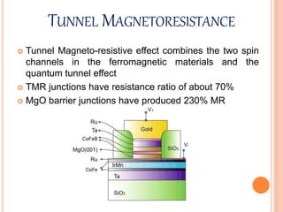
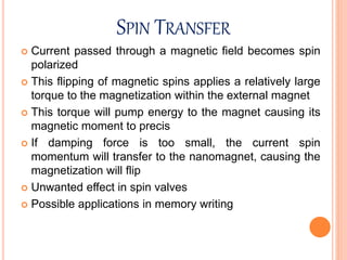
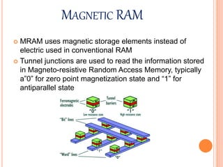
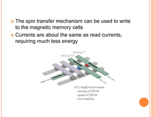
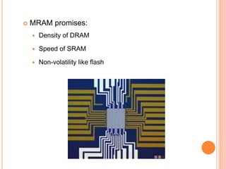
A Technical Seminar presentation
on
SPINTRONICS TECHNOLOGY
Presented By:
Felix
16Q91A0430
INTRODUCTION
 Conventional electronic devices
ignore the spin property and rely
strictly on the transport of the
electrical charge of electrons.
 Adding the spin degree of freedom
provides new effects, new
capabilities and new functionalities
FUTURE DEMANDS
 Moore’s Law states that the number of transistors on
a silicon chip will roughly double every eighteen
months
 As electronic devices become smaller, quantum
properties of the wavelike nature of electrons are no
longer negligible
 Spintronic devices offer the possibility of enhanced
functionality, higher speed, and reduced power
consumption
ADVANTAGES OF SPIN
 Information is stored into spin as one of two
possible orientations
 Spin lifetime is relatively long, on the order of
nanoseconds
 Spin currents can be manipulated
 Spin devices may combine logic and storage
functionality eliminating the need for separate
components
 Magnetic storage is non-volatile
 Binary spin polarization offers the possibility of
applications as qubits in quantum computers
GIANT MAGNETO-RESISTANCE
 1988 France, GMR discovery is
accepted as birth of spintronics
 A Giant Magneto-Resistive device is
made of at least two ferromagnetic
layers separated by a spacer layer
 When the magnetization of the two
outside layers is aligned, lowest
resistance
 Conversely, when magnetization
vectors are antiparallel, high R
 Small fields can produce big effects
 Parallel and perpendicular current
PARALLEL CURRENT GMR
 Current runs parallel between the ferromagnetic
layers
 Most commonly used in magnetic read heads
 Has shown 200% resistance difference between
zero point and antiparallel states
PERPENDICULAR CURRENT GMR
 Easier to understand theoretically, think of one FM
layer as spin polarizer and other as detector
 Has shown 70% resistance difference between
zero point and antiparallel states
 Basis for Tunneling MagnetoResistance
SPIN VALVE
 Simplest and most successful spintronic device
 Used in HDD to read information in the form of
small magnetic fields above the disk surface
TUNNEL MAGNETORESISTANCE
 Tunnel Magneto-resistive effect combines the two spin
channels in the ferromagnetic materials and the
quantum tunnel effect
 TMR junctions have resistance ratio of about 70%
 MgO barrier junctions have produced 230% MR
SPIN TRANSFER
 Current passed through a magnetic field becomes spin
polarized
 This flipping of magnetic spins applies a relatively large
torque to the magnetization within the external magnet
 This torque will pump energy to the magnet causing its
magnetic moment to precis
 If damping force is too small, the current spin
momentum will transfer to the nanomagnet, causing the
magnetization will flip
 Unwanted effect in spin valves
 Possible applications in memory writing
MAGNETIC RAM
 MRAM uses magnetic storage elements instead of
electric used in conventional RAM
 Tunnel junctions are used to read the information stored
in Magneto-resistive Random Access Memory, typically
a”0” for zero point magnetization state and “1” for
antiparallel state
 The spin transfer mechanism can be used to write
to the magnetic memory cells
 Currents are about the same as read currents,
requiring much less energy
 MRAM promises:
 Density of DRAM
 Speed of SRAM
 Non-volatility like flash
SPIN TRANSISTOR
 Ideal use of MRAM would utilize control of the spin
channels of the current
 Spin transistors would allow control of the spin
current in the same manner that conventional
transistors can switch charge currents
 Using arrays of these spin transistors, MRAM will
combine storage, detection, logic and
communication capabilities on a single chip
 This will remove the distinction between working
memory and storage, combining functionality of
many devices into one
MAGNETIC SEMICONDUCTORS
 Materials like magnetite are magnetic semiconductors
 Development of materials similar to conventional
 Research aimed at dilute magnetic semiconductors
 Manganese is commonly doped onto substrate
 However previous manganese-doped GaAs has
transition temp at -88oC
 Curie temperatures above room must be produced
CONCLUSION
o Interest in Spintronics arises, in part, from the looming
problem of exhausting the fundamental physical limits
of conventional electronics.
o Moreover, these "spintronic" devices might lead to
quantum computers and quantum communication
based on electronic solid-state devices, thus changing
the perspective of information technology in the 21st
century.
THANK
YOU

Spintronics Technology

  • 1.
    A Technical Seminarpresentation on SPINTRONICS TECHNOLOGY Presented By: Felix 16Q91A0430
  • 2.
    INTRODUCTION  Conventional electronicdevices ignore the spin property and rely strictly on the transport of the electrical charge of electrons.  Adding the spin degree of freedom provides new effects, new capabilities and new functionalities
  • 3.
    FUTURE DEMANDS  Moore’sLaw states that the number of transistors on a silicon chip will roughly double every eighteen months  As electronic devices become smaller, quantum properties of the wavelike nature of electrons are no longer negligible  Spintronic devices offer the possibility of enhanced functionality, higher speed, and reduced power consumption
  • 4.
    ADVANTAGES OF SPIN Information is stored into spin as one of two possible orientations  Spin lifetime is relatively long, on the order of nanoseconds  Spin currents can be manipulated  Spin devices may combine logic and storage functionality eliminating the need for separate components  Magnetic storage is non-volatile  Binary spin polarization offers the possibility of applications as qubits in quantum computers
  • 5.
    GIANT MAGNETO-RESISTANCE  1988France, GMR discovery is accepted as birth of spintronics  A Giant Magneto-Resistive device is made of at least two ferromagnetic layers separated by a spacer layer  When the magnetization of the two outside layers is aligned, lowest resistance  Conversely, when magnetization vectors are antiparallel, high R  Small fields can produce big effects  Parallel and perpendicular current
  • 6.
    PARALLEL CURRENT GMR Current runs parallel between the ferromagnetic layers  Most commonly used in magnetic read heads  Has shown 200% resistance difference between zero point and antiparallel states
  • 7.
    PERPENDICULAR CURRENT GMR Easier to understand theoretically, think of one FM layer as spin polarizer and other as detector  Has shown 70% resistance difference between zero point and antiparallel states  Basis for Tunneling MagnetoResistance
  • 8.
    SPIN VALVE  Simplestand most successful spintronic device  Used in HDD to read information in the form of small magnetic fields above the disk surface
  • 9.
    TUNNEL MAGNETORESISTANCE  TunnelMagneto-resistive effect combines the two spin channels in the ferromagnetic materials and the quantum tunnel effect  TMR junctions have resistance ratio of about 70%  MgO barrier junctions have produced 230% MR
  • 10.
    SPIN TRANSFER  Currentpassed through a magnetic field becomes spin polarized  This flipping of magnetic spins applies a relatively large torque to the magnetization within the external magnet  This torque will pump energy to the magnet causing its magnetic moment to precis  If damping force is too small, the current spin momentum will transfer to the nanomagnet, causing the magnetization will flip  Unwanted effect in spin valves  Possible applications in memory writing
  • 11.
    MAGNETIC RAM  MRAMuses magnetic storage elements instead of electric used in conventional RAM  Tunnel junctions are used to read the information stored in Magneto-resistive Random Access Memory, typically a”0” for zero point magnetization state and “1” for antiparallel state
  • 12.
     The spintransfer mechanism can be used to write to the magnetic memory cells  Currents are about the same as read currents, requiring much less energy
  • 13.
     MRAM promises: Density of DRAM  Speed of SRAM  Non-volatility like flash
  • 14.
    SPIN TRANSISTOR  Idealuse of MRAM would utilize control of the spin channels of the current  Spin transistors would allow control of the spin current in the same manner that conventional transistors can switch charge currents  Using arrays of these spin transistors, MRAM will combine storage, detection, logic and communication capabilities on a single chip  This will remove the distinction between working memory and storage, combining functionality of many devices into one
  • 15.
    MAGNETIC SEMICONDUCTORS  Materialslike magnetite are magnetic semiconductors  Development of materials similar to conventional  Research aimed at dilute magnetic semiconductors  Manganese is commonly doped onto substrate  However previous manganese-doped GaAs has transition temp at -88oC  Curie temperatures above room must be produced
  • 16.
    CONCLUSION o Interest inSpintronics arises, in part, from the looming problem of exhausting the fundamental physical limits of conventional electronics. o Moreover, these "spintronic" devices might lead to quantum computers and quantum communication based on electronic solid-state devices, thus changing the perspective of information technology in the 21st century.
  • 17.

Editor's Notes

  • #3 Spin does not replace charge current just provide extra control Using suitable materials, many different “bit” states can be interpreted
  • #4 New technology has been proposed which would involve a complete set of new materials, new handling and processing techniques, and altered circuit design. Such developments include single-electron transistors and molecular-electronic devices based on organic materials or carbon nanotubes.
  • #5 Charge state can be destroyed by interactions with impurities or other charges
  • #6 Think of optical polarizers
  • #10 230% with sputtering deposition
  • #12 Non volatile, instant-on computers
  • #14 DRAM stores one bit in only one capacitor and transistor, very dense but very power hungry because capacitor loses charge, must be frequently refreshed SRAM stores one bit in six transistors, faster than DRAM but less dense
  • #16  Ideally, each Mn dopant atom represents an acceptor that introduces a local spin and a hole carrier