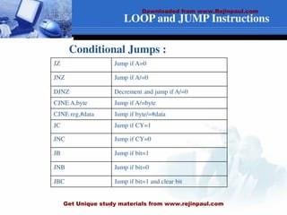
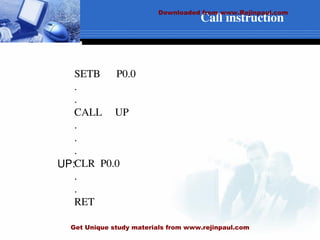
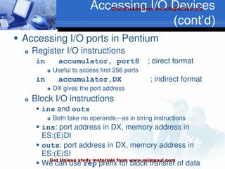
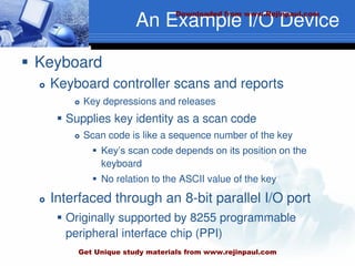
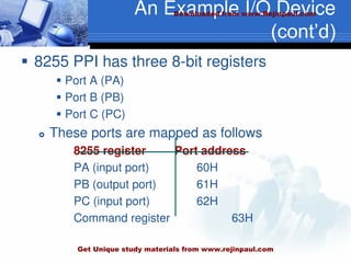
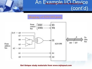
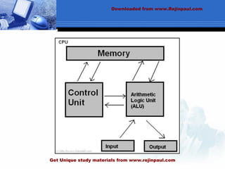
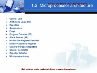
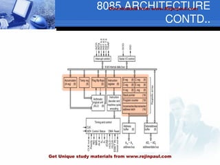
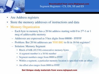
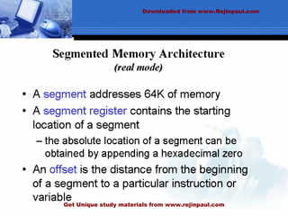
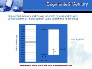
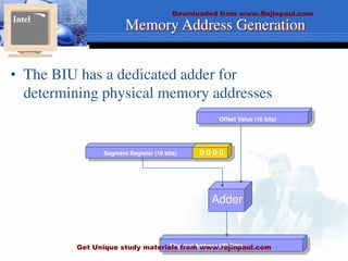
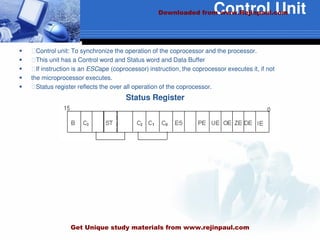
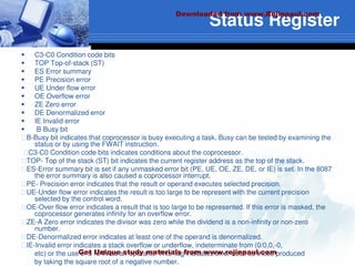
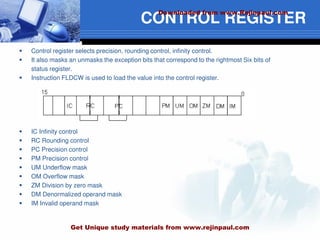
The document discusses the architecture and programming of 8-bit and 16-bit microprocessors. It covers the objectives of studying the architecture, instruction set, and peripheral interfacing of the 8085 and 8086 microprocessors. It provides details on the architecture, registers, instruction set, addressing modes of the 8085 microprocessor. It also discusses the architecture, registers, features, memory segmentation and addressing of the 8086 microprocessor.


![DEC byte ;byte=byte-1
INC byte ;byte=byte+1
INC R7
DEC A
DEC 40H ; [40]=[40]-1
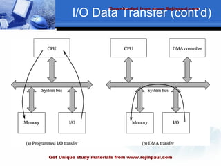
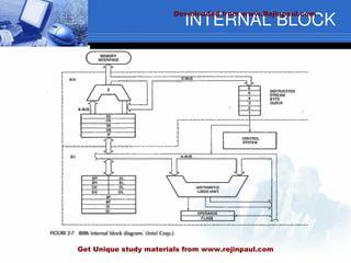
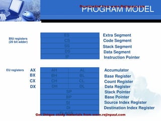
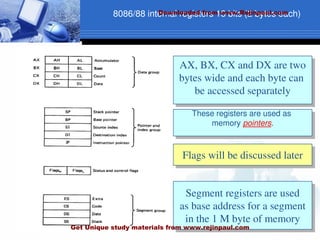
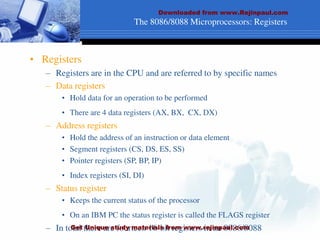
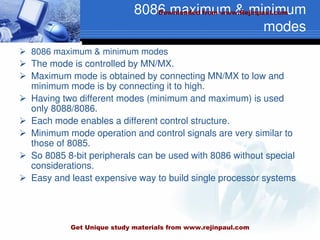
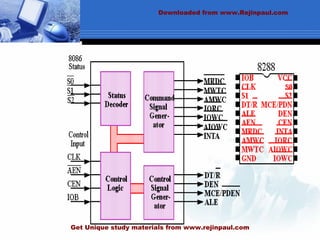
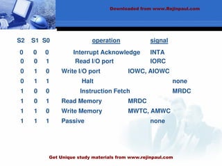
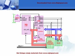
Downloaded from www.Rejinpaul.com
Get Unique study materials from www.rejinpaul.com](https://image.slidesharecdn.com/mpmccseppt-230425052706-3b1897bc/85/mpmc-cse-ppt-pdf-82-320.jpg)