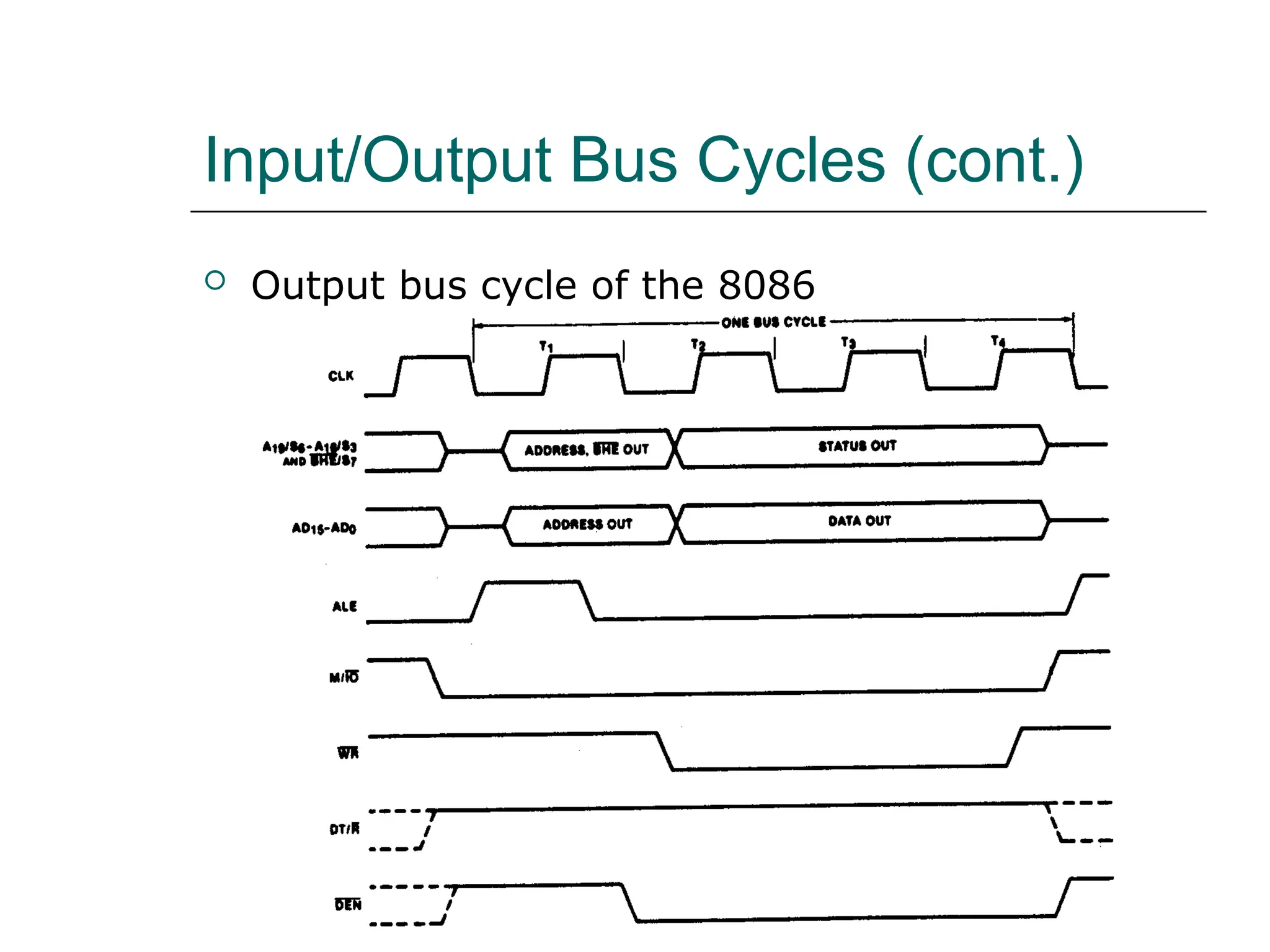
The 8088 and 8086
Microprocessors
 The 8086, announced in 1978, was the first 16-
bit microprocessor introduced by Intel
Corporation
 8086 and 8088 are internally 16-bit MPU.
 Externally the 8086 has a 16-bit data bus and
the 8088 has an 8-bit data bus
The 8088 and 8086
Microprocessors (cont.)
 8086 and 8088 both have the ability to address
up to 1 Mbyte of memory and 64K of
input/output port
 The 8088 and 8086 are both manufactured
using high-performance metal-oxide
semiconductor (HMOS) technology
 The 8088 and 8086 are housed in a 40-pin dual
inline package and many pins have multiple
functions
The 8088 and 8086
Microprocessors (cont.)
 CMOS, Complementary Metal-Oxide-
Semiconductor, is a major class of integrated
circuits used in chips such as microprocessors,
microcontrollers, static RAM, digital logic
circuits, and analog circuits such as image
sensors
 Two important characteristics of CMOS devices
are high noise immunity and low static power
supply drain.
 Significant power is only drawn when its
transistors are switching between on and off
states
The 8088 and 8086
Microprocessors (cont.)
 CMOS devices do not produce as much heat as
other forms of logic such as TTL.
 CMOS also allows a high density of logic
functions on a chip
The 8088 and 8086
Microprocessors (cont.)
Pin layout of the 8086 and 8088 microprocessor
• 16-bit Arithmetic Logic Unit
• 16-bit data bus (8088 has 8-bit data bus)
• 20-bit address bus - 220
= 1,048,576 = 1 meg
The address refers to a byte in memory. In the 8088, these bytes come in on
the 8-bit data bus. In the 8086, bytes at even addresses come in on the low
half of the data bus (bits 0-7) and bytes at odd addresses come in on the upper
half of the data bus (bits 8-15).
The 8086 can read a 16-bit word at an even address in one operation and at an
odd address in two operations. The 8088 needs two operations in either case.
The least significant byte of a word on an 8086 family microprocessor is at the
lower address.
8086 Features
Simplified CPU Design
Data Registers
Address Registers
Control
Unit
Arithmetic
Logic Unit
Status
Flags
Address Bus
Data Bus
Memory
CS
SS
DS
ES
Segment
BP
Index
SP
SI
DI
AH
BH
CH
DH DL
CL
BL
AL
General Purpose
Status and Control
Flags
IP
AX
BX
CX
DX
Intel 16-bit Registers
• The 8086 has two parts, the Bus Interface Unit (BIU) and the
Execution Unit (EU).
• The BIU fetches instructions, reads and writes data, and computes the
20-bit address.
• The EU decodes and executes the instructions using the 16-bit ALU.
• The BIU contains the following registers:
IP - the Instruction Pointer
CS - the Code Segment Register
DS - the Data Segment Register
SS - the Stack Segment Register
ES - the Extra Segment Register
The BIU fetches instructions using the CS and IP, written CS:IP, to contract
the 20-bit address. Data is fetched using a segment register (usually the DS)
and an effective address (EA) computed by the EU depending on the
addressing mode.
8086 Architecture
The EU contains the following 16-bit registers:
AX - the Accumulator
BX - the Base Register
CX - the Count Register
DX - the Data Register
SP - the Stack Pointer  defaults to stack segment
BP - the Base Pointer /
SI - the Source Index Register
DI - the Destination Register
These are referred to as general-purpose registers, although, as seen by
their names, they often have a special-purpose use for some instructions.
The AX, BX, CX, and DX registers can be considers as two 8-bit registers, a
High byte and a Low byte. This allows byte operations and compatibility with
the previous generation of 8-bit processors, the 8080 and 8085. 8085 source
code could be translated in 8086 code and assembled. The 8-bit registers are:
AX --> AH,AL
BX --> BH,BL
CX --> CH,CL
DX --> DH,DL
8086 Programmer’s Model
ES
CS
SS
DS
IP
AH
BH
CH
DH
AL
BL
CL
DL
SP
BP
SI
DI
FLAGS
AX
BX
CX
DX
Extra Segment
Code Segment
Stack Segment
Data Segment
Instruction Pointer
Accumulator
Base Register
Count Register
Data Register
Stack Pointer
Base Pointer
Source Index Register
Destination Index Register
BIU registers
(20 bit adder)
EU registers
8086/88 internal registers 16 bits (2 bytes each)
AX, BX, CX and DX are two
bytes wide and each byte can
be accessed separately
These registers are used as
memory pointers.
Flags will be discussed later
Segment registers are used
as base address for a segment
in the 1 M byte of memory
The 8086/8088 Microprocessors: Registers
• Registers
– Registers are in the CPU and are referred to by
specific names
– Data registers
• Hold data for an operation to be performed
• There are 4 data registers (AX, BX, CX, DX)
– Address registers
• Hold the address of an instruction or data element
• Segment registers (CS, DS, ES, SS)
• Pointer registers (SP, BP, IP)
• Index registers (SI, DI)
– Status register
• Keeps the current status of the processor
• On an IBM PC the status register is called the FLAGS
register
– In total there are fourteen 16-bit registers in an
Data Registers: AX, BX, CX, DX
• Instructions execute faster if the data is in a register
• AX, BX, CX, DX are the data registers
• Low and High bytes of the data registers can be accessed
separately
– AH, BH, CH, DH are the high bytes
– AL, BL, CL, and DL are the low bytes
• Data Registers are general purpose registers but they also perform
special functions
• AX
– Accumulator Register
– Preferred register to use in arithmetic, logic and data
transfer instructions because it generates the shortest
Machine Language Code
– Must be used in multiplication and division operations
– Must also be used in I/O operations
• BX
– Base Register
– Also serves as an address register
– Used in array operations
– Used in Table Lookup operations (XLAT)
• CX
– Count register
– Used as a loop counter
– Used in shift and rotate operations
• DX
– Data register
– Used in multiplication and division
– Also used in I/O operations
Pointer and Index Registers
• Contain the offset addresses of memory locations
• Can also be used in arithmetic and other operations
• SP: Stack pointer
– Used with SS to access the stack segment
• BP: Base Pointer
– Primarily used to access data on the stack
– Can be used to access data in other segments
• SI: Source Index register
– is required for some string operations
– When string operations are performed, the SI
register points to memory locations in the data
segment which is addressed by the DS register.
Thus, SI is associated with the DS in string
operations.
• DI: Destination Index register
– is also required for some string operations.
– When string operations are performed, the DI
register points to memory locations in the data
segment which is addressed by the ES register.
Thus, DI is associated with the ES in string
operations.
• The SI and the DI registers may also be used to access data
stored in arrays
Segment Registers - CS, DS, SS and ES
• Are Address registers
• Store the memory addresses of instructions and data
• Memory Organization
– Each byte in memory has a 20 bit address starting with
0 to 220
-1 or 1 meg of addressable memory
– Addresses are expressed as 5 hex digits from 00000 -
FFFFF
– Problem: But 20 bit addresses are TOO BIG to fit in 16
bit registers!
– Solution: Memory Segment
• Block of 64K (65,536) consecutive memory bytes
• A segment number is a 16 bit number
• Segment numbers range from 0000 to FFFF
• Within a segment, a particular memory location is specified
with an offset
• An offset also ranges from 0000 to FFFF
Segmented Memory
Segmented memory addressing: absolute (linear) address is a
combination of a 16-bit segment value added to a 16-bit offset
linear
addresses
one segment
Memory Address
Generation
• The BIU has a dedicated adder for
determining physical memory
addresses
Intel
Physical Address (20 Bits)
Adder
Segment Register (16 bits) 0 0 0 0
Offset Value (16 bits)
Example Address
Calculation
• If the data segment starts at
location 1000h and a data
reference contains the address 29h
where is the actual data?
Intel
Offset: 0 0 0 0 0 0 0 0 0 0 1 0 1 0 0 1
2 9
0 0 0 1 0 0 0 0 0 0 0 0 0 0 0 0 0 0 0 0
Segment:
0 0 0 1 0 0 0 0 0 0 0 0 0 0 1 0 1 0 0 1
Address:
Segment:Offset Address
• Logical Address is specified as segment:offset
• Physical address is obtained by shifting the segment address 4
bits to the left and adding the offset address
• Thus the physical address of the logical address A4FB:4872 is
A4FB0
+ 4872
A9822
Your turn . . .
What linear address corresponds to the segment/offset
address 028F:0030?
028F0 + 0030 = 02920
Always use hexadecimal notation for addresses.
Your turn . . .
What segment addresses correspond to the linear address
28F30h?
Many different segment-offset addresses can produce the
linear address 28F30h. For example:
28F0:0030, 28F3:0000, 28B0:0430, . . .
The Code Segment
Memory
Segment Register
Offset
Physical or
Absolute Address
0
+
CS:
IP
0400H
0056H
4000H
4056H
0400
0056
04056H
The offset is the distance in bytes from the start of the segment.
The offset is given by the IP for the Code Segment.
Instructions are always fetched with using the CS register.
CS:IP = 400:56
Logical Address
0H
0FFFFFH
The physical address is also called the absolute address.
The Data Segment
Memory
Segment Register
Offset
Physical Address
+
DS:
EA
05C0
0050
05C00H
05C50H
05C0 0
0050
05C50H
Data is usually fetched with respect to the DS register.
The effective address (EA) is the offset.
The EA depends on the addressing mode.
DS:EA
0H
0FFFFFH
The Stack Segment
Memory
Segment Register
Offset
Physical Address
+
SS:
SP
0A00
0100
0A000H
0A100H
0A00 0
0100
0A100H
The stack is always referenced with respect to the stack segment register.
The stack grows toward decreasing memory locations.
The SP points to the last or top item on the stack.
PUSH - pre-decrement the SP
POP - post-increment the SP
The offset is given by the SP register.
SS:SP
0H
0FFFFFH
Flags
Carry flag
Parity flag
Auxiliary flag
Zero
Overflow
Direction
Interrupt enable
Trap
Sign
6 are status flags
3 are control flag
• CF (carry) Contains carry from leftmost bit following
arithmetic, also contains last bit from a shift or rotate
operation.
Flag Register
Flag O D I T S Z A P C
Bit no. 15 14 13 12 11
1
0
9 8 7 6 5 4 3 2 1 0
• Conditional flags:
– They are set according to some results of arithmetic
operation. You do not need to alter the value yourself.
• Control flags:
– Used to control some operations of the MPU. These flags
are to be set by you in order to achieve some specific
purposes.
Flag Register
• OF (overflow) Indicates overflow of
the leftmost bit during arithmetic.
• DF (direction) Indicates left or
right for moving or comparing
string data.
• IF (interrupt) Indicates whether
external interrupts are being
processed or ignored.
• TF (trap) Permits operation of the
processor in single step mode.
• SF (sign) Contains the resulting
sign of an arithmetic operation
(1=negative)
• ZF (zero) Indicates when the result
of arithmetic or a comparison is
zero. (1=yes)
• AF (auxiliary carry) Contains carry
out of bit 3 into bit 4 for
specialized arithmetic.
• PF (parity) Indicates the number of
1 bits that result from an
operation.
Minimum-Mode and Maximum-
Mode System
Minimum-Mode and Maximum-
Mode System (cont.)
Signals common to both minimum and maximum mode
Minimum-Mode and Maximum-
Mode System (cont.)
Unique minimum-mode signals
Minimum-Mode and Maximum-
Mode System (cont.)
Unique maximum-mode signals
Minimum-Mode and Maximum-
Mode System (cont.)
Minimum-Mode Interface
Block diagram of the minimum-mode 8088 MPU
Minimum-Mode Interface (cont.)
Block diagram of the minimum-mode 8086 MPU
Minimum-Mode Interface (cont.)
 The minimum-mode signals can be divided into
the following basic groups:
 Address/Data bus
 Status signals
 Control signals
 Interrupt signals
 DMA interface signals
Minimum-Mode Interface (cont.)
 Address/Data bus
 The address bus is used to carry address information to
the memory and I/O ports
 The address bus is 20-bit long and consists of signal lines
A0 through A19
 A 20-bit address gives the 8088 a 1 Mbyte memory
address space
 Only address line A0 through A15 are used when
addressing I/O.
 This give an I/O address space of 64 Kbytes
 The 8088 has 8 multiplexed address/data bus lines
(A0~A7)
 8086 has 16 multiplexed address/data bus lines (A0~A15)
Minimum-Mode Interface (cont.)
 Status signals
 The four most significant address, A19 through A16
are multiplexed with status signal S6 through S3
 Bits S4 and S3 together form a 2-bit binary code
that identifies which of the internal segment
registers was used to generate the physical
address.
 S5 is the logic level of the internal interrupt flag.
 S6 is always at the 0 logic level
Minimum-Mode Interface (cont.)
Maximum-Mode Interface
 The maximum-mode configuration is mainly used
for implementing a multiprocessor/coprocessor
system environment
 Multiple processors exist in the system
 Each executes its own program
 Global resources and local resources
 The former are common to all processors
 The latter are assigned to specific processors
 In the maximum-mode, facilities are provided for
implementing allocation of global resources and
passing bus control to other microprocessors
sharing the system bus
Maximum-Mode Interface (cont.)
8088 maximum-mode block diagram
Maximum-Mode Interface (cont.)
8086 maximum-mode block diagram
Maximum-Mode Interface (cont.)
 8288 bus controller
Block diagram and pin layout of 8288
Maximum-Mode Interface (cont.)
 8288 bus controller
 In the maximum-mode, 8088/8086 outputs a
status code on three signal line, S0, S1, S2, prior
to the initialization of each bus cycle
 The 3-bit bus status code identifies which type of
bus cycle is to follow and are input to the
external bus controller device, 8288
 The 8288 produces one or two command signals
for each bus cycle
Maximum-Mode Interface (cont.)
 8288 bus controller
Bus status code
Maximum-Mode Interface (cont.)
 Queue status signals
 The 2-bit queue status code QS0 and QS1 tells
the external circuitry what type of information
was removed form the queue during the previous
clock cycle
Queue status code
Electrical Characteristics
 Power is applied between pin 40 (Vcc) and pins
1 (GND) and 20 (GND)
 The nominal value of Vcc is specified as +5V dc
with a tolerance of ±10%.
 Both 8088 and 8086 draw a maximum of
340mA from the supply
I/O voltage levels
System Clock
 The time base for synchronization of the
internal and external operations of the
microprocessor in a microcomputer system is
provided by the clock (CLK) input signal
 The standard 8088 operates at 5 MHz and the
8088-2 operates at 8 MHz
 The 8086 is manufactured in three speeds: 5-
MHz 8086, 8-MHz 8086-2, and the 10-MHz
8086-1
 The CLK is externally generated by the 8284
clock generator and driver IC
System Clock (cont.)
 Block diagram of the 8284 clock generator
System Clock (cont.)
 Block diagram of the 8284 clock generator
System Clock (cont.)
 Connecting the 8284 to the 8088
15- or 24MHz
crystal
Typical value of CL when used with
15MHz crystal is 12pF
The fundamental crystal frequency is divided
by 3 within the 8284 to give either a 5- or 8-
MHz clock signal
System Clock (cont.)
 CLK waveform
 The signal is specified at Metal Oxide
Semiconductor (MOS)-compatible voltage level
 The period of the 5-MHz 8088 can range from
200 ns to 500 ns, and the maximum rise and fall
times of its edges equal 10 ns
System Clock (cont.)
 PCLK and OSC signals
 The peripheral clock (PCLK) and oscillator clock
(OSC) signals are provided to drive peripheral
ICs
 The clock output at PCLK is half the frequency of
CLK. The OSC output is at the crystal frequency
which is three times of CLK
System Clock (cont.)
 The 8284 can also be driven from an external
clock source
 Applied to the EFI (External Frequency Input)
 Input F/C is used for selection
 0: crystal between X1 and X2 is used
 1: selects EFI
 The CSYNC input is used for external
synchronization in systems with multiple
clocks
System Clock (cont.)
 EXAMPLE
 If the CLK input of an 8086 MPU is to be driven
by a 9-MHz signal, what speed version of the
8086 must be used and what frequency crystal
must be attached to the 8284
 Solution:
 The 8086-1 is the version of the 8086 that can
be run at 9-MHz. To create the 9-MHz clock, a
27-MHz crystal must be used on the 8284.
Bus Cycle and Time States
 A bus cycle defines the basic operation that a
microprocessor performs to communicate with
external devices.
 Examples of bus cycles are the memory read,
memory write, input/output read, and
input/output write.
 The bus cycle of the 8088 and 8086
microprocessors consists of at least four clock
periods.
 If no bus cycles are required, the microprocessor
performs what are known as idle states.
 When READY is held at the 0 level, wait states
are inserted between states T3 and T4 of the bus
cycle.
Bus Cycle and Time States (cont.)
Bus cycle clock periods, idle state, and wait state
Bus Cycle and Time States (cont.)
 EXAMPLE
 What is the duration of the bus cycle in the 8088-
based microcomputer if the clock is 8 MHz and the
two wait states are inserted.
 Solution:
 The duration of the bus cycle in an 8 MHz system
is given by
 tcyc = 500 ns + N x 125 ns
 In this expression the N stands for the number of
waits states. For a bus cycle with two wait states,
we get
 tcyc = 500 ns + 2 x 125 ns = 500 ns + 250 ns =
750 ns
Hardware Organization of the
Memory Address Space
1Mx8 memory bank of the 8088
Hardware Organization of the
Memory Address Space (cont.)
High and low memory banks of the 8086
Hardware Organization of the
Memory Address Space (cont.)
Byte transfer by the 8088
Hardware Organization of the
Memory Address Space (cont.)
Word transfer by the 8088
Hardware Organization of the
Memory Address Space (cont.)
Even address byte transfer by the 8086
Hardware Organization of the
Memory Address Space (cont.)
Odd address byte transfer by the 8086
Hardware Organization of the
Memory Address Space (cont.)
Even address word transfer by the 8086
Hardware Organization of the
Memory Address Space (cont.)
Odd-address word transfer by the 8086
Hardware Organization of the
Memory Address Space (cont.)
 EXAMPLE
 Is the word at memory address 0123116 of an
8086-based microcomputer aligned or
misaligned? How many cycle are required to read
it from memory?
 Solution:
 The first byte of the word is the second byte at
the aligned-word address 0123016. Therefore, the
word is misaligned and required two bus cycles
to be read from memory.
Address Bus Status Codes
 Whenever a memory bus cycle is in progress,
an address bus status code S4S3 is output by
the processor.
 S4S3 identifies which one of the four segment
register is used to generate the physical
address in the current bus cycle: 􀂙
 S4S3=00 identifies the extra segment register
(ES)
 S4S3=01 identifies the stack segment
register (SS)
 S4S3=10 identifies the code segment register
(CS)
 S4S3=11 identifies the data segment register
(DS)
 The memory address reach of the
microprocessor can thus be expanded to 4
Mbytes.
Memory Control Signals
 Minimum-mode memory control signals
Memory Control Signals (cont.)
 Minimum-mode memory control signals (8088)
 ALE – Address Latch Enable – used to latch
the address in external memory.
 IO/M – Input-Output/Memory – signal
external circuitry whether a memory of I/O bus
cycle is in progress.
 DT/R – Data Transmit/Receive – signal
external circuitry whether the 8088 is
transmitting or receiving data over the bus. 􀂙
 RD – Read – identifies that a read bus cycle is in
progress.
 WR – Write – identifies that a write bus cycle is
in progress.
 DEN – Data Enable – used to enable the data
bus. 􀂙
 SSO – Status Line – identifies whether a code or
data access is in progress.
Memory Control Signals (cont.)
 The control signals for the 8086’s minimum-
mode memory interface differs in three ways:
 IO/M signal is replaced by M/IO signal.
 The signal SSO is removed from the interface.
 BHE (bank high enable) is added to the interface
and is used to select input for the high bank of
memory in the 8086’s memory subsystem.
Memory Control Signals (cont.)
 Maximum-mode memory control signals
Memory Control Signals (cont.)
 Maximum-mode memory control signals
 MRDC – Memory Read Command 􀂙
 MWTC – Memory Write Command 􀂙
 AMWC – Advanced Memory Write Command
Read and Write Bus Cycle
 Read cycle
Minimum-mode memory read bus cycle of the 8088
Read and Write Bus Cycle (cont.)
 Read cycle
Minimum-mode memory read bus cycle of the 8086
Read and Write Bus Cycle (cont.)
 Read cycle
Maximum-mode memory read bus cycle of the 8086
Read and Write Bus Cycle (cont.)
 Write cycle
Minimum-mode memory write bus cycle of the 8088
Read and Write Bus Cycle (cont.)
 Write cycle
Maximum-mode memory write bus cycle of the 8086
Memory Interface Circuit
 Address bus latches and buffers
 Bank write and bank read control logic
 Data bus transceivers/buffers
 Address decoders
Memory Interface Circuit (cont.)
Memory interface block diagram
Memory Interface Circuit (cont.)
 Address bus latches and buffers
Block diagram of a D-type latch
Memory Interface Circuit (cont.)
 Address bus latches and buffers
Circuit diagram of the 74F373
Memory Interface Circuit (cont.)
 A review of flip-flop/latch logic
Positive edge-triggered D flip-flop
Memory Interface Circuit (cont.)
 A review of flip-flop/latch logic
Positive edge-triggered JK flip-flop
Memory Interface Circuit (cont.)
 A review of flip-flop/latch logic
D-type latch
Memory Interface Circuit (cont.)
 Address bus latches and buffers
Address latch circuit
Memory Interface Circuit (cont.)
 Bank write and bank read control logic
Bank write control logic Bank read control logic
Memory Interface Circuit (cont.)
 Data bus transceivers
Block diagram and circuit
diagram of the 74F245 octal bus
transceiver
Memory Interface Circuit (cont.)
 Data bus transceivers
Data bus transceiver circuit
Memory Interface Circuit (cont.)
 Address decoder
Address bus configuration with address decoding
Memory Interface Circuit (cont.)
 Address decoder
Block diagram and operation of the 74F139 decoder
Memory Interface Circuit (cont.)
 Address decoder
Circuit diagram of the 74F139 decoder
Memory Interface Circuit (cont.)
 Address decoder
Address decoder circuit using 74F139
Memory Interface Circuit (cont.)
 Address decoder
Block diagram and operation of the 74F138 decoder
Memory Interface Circuit (cont.)
 Address decoder
Circuit diagram of the 74F138 decoder
Memory Interface Circuit (cont.)
 Address decoder
Address decoder circuit using 74F138
Types of Input/Output
 The I/O system allows peripherals to provide
data or receive results of processing the data
 Using I/O ports
 The 8088/8086 MPU can employ two types
of I/O
 Isolated I/O
 Memory-mapped I/O
 They differ in how I/O ports are mapped into the
address space
Types of Input/Output (cont.)
 Isolated input/output
 When using isolated I/O in a microcomputer
system, the I/O device are treated separate from
memory
 The memory address space contains 1 M consecutive
byte address in the range 0000016 through FFFFF16
 The I/O address space contains 64K consecutive byte
addresses in the range 000016 through FFFF16
 The bytes in two consecutive I/O addresses can
be accessed as word-wide data
 Page 0: 000016  00FF16
 Certain I/O instructions can only perform in this range
Types of Input/Output (cont.)
 Isolated input/output
8088/8086 memory and I/O address spaces
Types of Input/Output (cont.)
 Isolated input/output
Isolated I/O ports
Types of Input/Output (cont.)
 Isolated input/output
 Advantages:
 The complete 1Mbyte memory address space is
available for use with memory
 Special instructions have been provided to perform
I/O operations with maximized performance
 The bytes in two consecutive I/O addresses can
be accessed as word-wide data
 Disadvantages:
 All input and output data transfers must take place
between the AL or AX register and I/O port
Types of Input/Output (cont.)
 Memory-mapped input/output
 MPU looks at the I/O port as though it is a storage
location in memory
 Some of the memory address space is dedicated to I/O ports
 Instructions that affect data in memory are used
instead of the special I/O instructions
 More instructions and addressing modes are available to
perform I/O operations
 I/O transfers can take place between I/O port and other
internal registers
 The memory instructions tend to execute slower than
those specifically designed for isolated I/O
 Part of the memory address space is lost
Types of Input/Output(cont.)
 Memory-mapped input/output
Memory mapped I/O ports
Isolated Input/Output Interface
 I/O devices:
 Keyboard
 Printer
 Mouse
 82C55A, etc
 Functions of interface circuit:
 Select the I/O port
 Latch output data
 Sample input data
 Synchronize data transfer
 Translate between TTL voltage levels and those
required to operate the I/O devices
Isolated Input/Output Interface
(cont.)
 Minimum-mode interface
Minimum-mode 8088 system I/O interface
Isolated Input/Output Interface
(cont.)
 Minimum-mode interface
Minimum-mode 8086 system I/O interface
Isolated Input/Output Interface
(cont.)
 Maximum-mode interface
Maximum-mode 8088 system I/O interface
Isolated Input/Output Interface
(cont.)
 Maximum-mode interface
Maximum-mode 8086 system I/O interface
Isolated Input/Output Interface
(cont.)
 Maximum-mode interface
I/O bus cycle status codes
Input/Output Data Transfer
 Input/output data transfers in the 8088 and 8086
microcomputers can be either byte-wide or word-wide
 I/O addresses are 16 bits in length and are output by
the 8088 to the I/O interface over bus lines AD0
through AD7 and A8 through A15
 In 8088, the word transfers is performed as two
consecutive byte-wide data transfer and takes two
bus cycle
 In 8086, the word transfers can takes either one or
two bus cycle
 Word-wide I/O ports should be aligned at even-
address boundaries
Input/Output Data Instructions
(cont.)
EXAMPLE:
 Write a sequence of instructions that will output
the data FF16 to a byte-wide output port at
address AB16 of the I/O address space.
Solution:
 First, the AL register is loaded with FF16 as an
immediate operand in the instruction
MOV AL, 0FFH
 Now the data in AL can be output to the byte-
wide output port with the instruction
OUT 0ABH, AL
Input/Output Data Instructions
(cont.)
EXAMPLE:
 Write a series of instructions that will output FF16 to an
output port located at address B00016 of the I/O address
space
Solution:
 The DX register must first be loaded with the address of
the output port. This is done with the instruction
MOV DX, 0B000H
 Next, the data that are to be output must be loaded into
AL with the instruction
MOV AL, 0FFH
 Finally, the data are output with the instruction
OUT DX, AL
Input/Output Data Instructions
(cont.)
EXAMPLE:
 Data are to be read in from two byte-wide input
ports at addresses AA16 and A916 and then output
as a word-wide output port at address B00016.
Write a sequence of instructions to perform this
input/output operation.
Input/Output Data Instructions
(cont.)
Solution:
 First read in the byte at address AA16 into AL and
move it into AH.
IN AL, 0AAH
MOV AH, AL
 Now the other byte can be read into AL by the
instruction
IN AL, 09AH
 And to write out the word of data
MOV DX, 0B000H
OUT DX, AX
Input/Output Bus Cycles
 Input bus cycle of the 8088
Input/Output Bus Cycles (cont.)
 Output bus cycle of the 8088
Input/Output Bus Cycles (cont.)
 Input bus cycle of the 8086
Input/Output Bus Cycles (cont.)
 Output bus cycle of the 8086

8086 microprocessor and 8088 microprocessor

  • 1.
    The 8088 and8086 Microprocessors  The 8086, announced in 1978, was the first 16- bit microprocessor introduced by Intel Corporation  8086 and 8088 are internally 16-bit MPU.  Externally the 8086 has a 16-bit data bus and the 8088 has an 8-bit data bus
  • 2.
    The 8088 and8086 Microprocessors (cont.)  8086 and 8088 both have the ability to address up to 1 Mbyte of memory and 64K of input/output port  The 8088 and 8086 are both manufactured using high-performance metal-oxide semiconductor (HMOS) technology  The 8088 and 8086 are housed in a 40-pin dual inline package and many pins have multiple functions
  • 3.
    The 8088 and8086 Microprocessors (cont.)  CMOS, Complementary Metal-Oxide- Semiconductor, is a major class of integrated circuits used in chips such as microprocessors, microcontrollers, static RAM, digital logic circuits, and analog circuits such as image sensors  Two important characteristics of CMOS devices are high noise immunity and low static power supply drain.  Significant power is only drawn when its transistors are switching between on and off states
  • 4.
    The 8088 and8086 Microprocessors (cont.)  CMOS devices do not produce as much heat as other forms of logic such as TTL.  CMOS also allows a high density of logic functions on a chip
  • 5.
    The 8088 and8086 Microprocessors (cont.) Pin layout of the 8086 and 8088 microprocessor
  • 6.
    • 16-bit ArithmeticLogic Unit • 16-bit data bus (8088 has 8-bit data bus) • 20-bit address bus - 220 = 1,048,576 = 1 meg The address refers to a byte in memory. In the 8088, these bytes come in on the 8-bit data bus. In the 8086, bytes at even addresses come in on the low half of the data bus (bits 0-7) and bytes at odd addresses come in on the upper half of the data bus (bits 8-15). The 8086 can read a 16-bit word at an even address in one operation and at an odd address in two operations. The 8088 needs two operations in either case. The least significant byte of a word on an 8086 family microprocessor is at the lower address. 8086 Features
  • 7.
    Simplified CPU Design DataRegisters Address Registers Control Unit Arithmetic Logic Unit Status Flags Address Bus Data Bus Memory
  • 8.
    CS SS DS ES Segment BP Index SP SI DI AH BH CH DH DL CL BL AL General Purpose Statusand Control Flags IP AX BX CX DX Intel 16-bit Registers
  • 9.
    • The 8086has two parts, the Bus Interface Unit (BIU) and the Execution Unit (EU). • The BIU fetches instructions, reads and writes data, and computes the 20-bit address. • The EU decodes and executes the instructions using the 16-bit ALU. • The BIU contains the following registers: IP - the Instruction Pointer CS - the Code Segment Register DS - the Data Segment Register SS - the Stack Segment Register ES - the Extra Segment Register The BIU fetches instructions using the CS and IP, written CS:IP, to contract the 20-bit address. Data is fetched using a segment register (usually the DS) and an effective address (EA) computed by the EU depending on the addressing mode. 8086 Architecture
  • 10.
    The EU containsthe following 16-bit registers: AX - the Accumulator BX - the Base Register CX - the Count Register DX - the Data Register SP - the Stack Pointer defaults to stack segment BP - the Base Pointer / SI - the Source Index Register DI - the Destination Register These are referred to as general-purpose registers, although, as seen by their names, they often have a special-purpose use for some instructions. The AX, BX, CX, and DX registers can be considers as two 8-bit registers, a High byte and a Low byte. This allows byte operations and compatibility with the previous generation of 8-bit processors, the 8080 and 8085. 8085 source code could be translated in 8086 code and assembled. The 8-bit registers are: AX --> AH,AL BX --> BH,BL CX --> CH,CL DX --> DH,DL
  • 12.
    8086 Programmer’s Model ES CS SS DS IP AH BH CH DH AL BL CL DL SP BP SI DI FLAGS AX BX CX DX ExtraSegment Code Segment Stack Segment Data Segment Instruction Pointer Accumulator Base Register Count Register Data Register Stack Pointer Base Pointer Source Index Register Destination Index Register BIU registers (20 bit adder) EU registers
  • 13.
    8086/88 internal registers16 bits (2 bytes each) AX, BX, CX and DX are two bytes wide and each byte can be accessed separately These registers are used as memory pointers. Flags will be discussed later Segment registers are used as base address for a segment in the 1 M byte of memory
  • 14.
    The 8086/8088 Microprocessors:Registers • Registers – Registers are in the CPU and are referred to by specific names – Data registers • Hold data for an operation to be performed • There are 4 data registers (AX, BX, CX, DX) – Address registers • Hold the address of an instruction or data element • Segment registers (CS, DS, ES, SS) • Pointer registers (SP, BP, IP) • Index registers (SI, DI) – Status register • Keeps the current status of the processor • On an IBM PC the status register is called the FLAGS register – In total there are fourteen 16-bit registers in an
  • 15.
    Data Registers: AX,BX, CX, DX • Instructions execute faster if the data is in a register • AX, BX, CX, DX are the data registers • Low and High bytes of the data registers can be accessed separately – AH, BH, CH, DH are the high bytes – AL, BL, CL, and DL are the low bytes • Data Registers are general purpose registers but they also perform special functions • AX – Accumulator Register – Preferred register to use in arithmetic, logic and data transfer instructions because it generates the shortest Machine Language Code – Must be used in multiplication and division operations – Must also be used in I/O operations
  • 16.
    • BX – BaseRegister – Also serves as an address register – Used in array operations – Used in Table Lookup operations (XLAT) • CX – Count register – Used as a loop counter – Used in shift and rotate operations • DX – Data register – Used in multiplication and division – Also used in I/O operations
  • 17.
    Pointer and IndexRegisters • Contain the offset addresses of memory locations • Can also be used in arithmetic and other operations • SP: Stack pointer – Used with SS to access the stack segment • BP: Base Pointer – Primarily used to access data on the stack – Can be used to access data in other segments • SI: Source Index register – is required for some string operations – When string operations are performed, the SI register points to memory locations in the data segment which is addressed by the DS register. Thus, SI is associated with the DS in string operations.
  • 18.
    • DI: DestinationIndex register – is also required for some string operations. – When string operations are performed, the DI register points to memory locations in the data segment which is addressed by the ES register. Thus, DI is associated with the ES in string operations. • The SI and the DI registers may also be used to access data stored in arrays
  • 19.
    Segment Registers -CS, DS, SS and ES • Are Address registers • Store the memory addresses of instructions and data • Memory Organization – Each byte in memory has a 20 bit address starting with 0 to 220 -1 or 1 meg of addressable memory – Addresses are expressed as 5 hex digits from 00000 - FFFFF – Problem: But 20 bit addresses are TOO BIG to fit in 16 bit registers! – Solution: Memory Segment • Block of 64K (65,536) consecutive memory bytes • A segment number is a 16 bit number • Segment numbers range from 0000 to FFFF • Within a segment, a particular memory location is specified with an offset • An offset also ranges from 0000 to FFFF
  • 21.
    Segmented Memory Segmented memoryaddressing: absolute (linear) address is a combination of a 16-bit segment value added to a 16-bit offset linear addresses one segment
  • 22.
    Memory Address Generation • TheBIU has a dedicated adder for determining physical memory addresses Intel Physical Address (20 Bits) Adder Segment Register (16 bits) 0 0 0 0 Offset Value (16 bits)
  • 23.
    Example Address Calculation • Ifthe data segment starts at location 1000h and a data reference contains the address 29h where is the actual data? Intel Offset: 0 0 0 0 0 0 0 0 0 0 1 0 1 0 0 1 2 9 0 0 0 1 0 0 0 0 0 0 0 0 0 0 0 0 0 0 0 0 Segment: 0 0 0 1 0 0 0 0 0 0 0 0 0 0 1 0 1 0 0 1 Address:
  • 24.
    Segment:Offset Address • LogicalAddress is specified as segment:offset • Physical address is obtained by shifting the segment address 4 bits to the left and adding the offset address • Thus the physical address of the logical address A4FB:4872 is A4FB0 + 4872 A9822
  • 26.
    Your turn .. . What linear address corresponds to the segment/offset address 028F:0030? 028F0 + 0030 = 02920 Always use hexadecimal notation for addresses.
  • 27.
    Your turn .. . What segment addresses correspond to the linear address 28F30h? Many different segment-offset addresses can produce the linear address 28F30h. For example: 28F0:0030, 28F3:0000, 28B0:0430, . . .
  • 28.
    The Code Segment Memory SegmentRegister Offset Physical or Absolute Address 0 + CS: IP 0400H 0056H 4000H 4056H 0400 0056 04056H The offset is the distance in bytes from the start of the segment. The offset is given by the IP for the Code Segment. Instructions are always fetched with using the CS register. CS:IP = 400:56 Logical Address 0H 0FFFFFH The physical address is also called the absolute address.
  • 29.
    The Data Segment Memory SegmentRegister Offset Physical Address + DS: EA 05C0 0050 05C00H 05C50H 05C0 0 0050 05C50H Data is usually fetched with respect to the DS register. The effective address (EA) is the offset. The EA depends on the addressing mode. DS:EA 0H 0FFFFFH
  • 30.
    The Stack Segment Memory SegmentRegister Offset Physical Address + SS: SP 0A00 0100 0A000H 0A100H 0A00 0 0100 0A100H The stack is always referenced with respect to the stack segment register. The stack grows toward decreasing memory locations. The SP points to the last or top item on the stack. PUSH - pre-decrement the SP POP - post-increment the SP The offset is given by the SP register. SS:SP 0H 0FFFFFH
  • 31.
    Flags Carry flag Parity flag Auxiliaryflag Zero Overflow Direction Interrupt enable Trap Sign 6 are status flags 3 are control flag
  • 32.
    • CF (carry)Contains carry from leftmost bit following arithmetic, also contains last bit from a shift or rotate operation. Flag Register Flag O D I T S Z A P C Bit no. 15 14 13 12 11 1 0 9 8 7 6 5 4 3 2 1 0 • Conditional flags: – They are set according to some results of arithmetic operation. You do not need to alter the value yourself. • Control flags: – Used to control some operations of the MPU. These flags are to be set by you in order to achieve some specific purposes.
  • 33.
    Flag Register • OF(overflow) Indicates overflow of the leftmost bit during arithmetic. • DF (direction) Indicates left or right for moving or comparing string data. • IF (interrupt) Indicates whether external interrupts are being processed or ignored. • TF (trap) Permits operation of the processor in single step mode.
  • 34.
    • SF (sign)Contains the resulting sign of an arithmetic operation (1=negative) • ZF (zero) Indicates when the result of arithmetic or a comparison is zero. (1=yes) • AF (auxiliary carry) Contains carry out of bit 3 into bit 4 for specialized arithmetic. • PF (parity) Indicates the number of 1 bits that result from an operation.
  • 37.
  • 38.
    Minimum-Mode and Maximum- ModeSystem (cont.) Signals common to both minimum and maximum mode
  • 39.
    Minimum-Mode and Maximum- ModeSystem (cont.) Unique minimum-mode signals
  • 40.
    Minimum-Mode and Maximum- ModeSystem (cont.) Unique maximum-mode signals
  • 41.
  • 42.
    Minimum-Mode Interface Block diagramof the minimum-mode 8088 MPU
  • 43.
    Minimum-Mode Interface (cont.) Blockdiagram of the minimum-mode 8086 MPU
  • 44.
    Minimum-Mode Interface (cont.) The minimum-mode signals can be divided into the following basic groups:  Address/Data bus  Status signals  Control signals  Interrupt signals  DMA interface signals
  • 45.
    Minimum-Mode Interface (cont.) Address/Data bus  The address bus is used to carry address information to the memory and I/O ports  The address bus is 20-bit long and consists of signal lines A0 through A19  A 20-bit address gives the 8088 a 1 Mbyte memory address space  Only address line A0 through A15 are used when addressing I/O.  This give an I/O address space of 64 Kbytes  The 8088 has 8 multiplexed address/data bus lines (A0~A7)  8086 has 16 multiplexed address/data bus lines (A0~A15)
  • 46.
    Minimum-Mode Interface (cont.) Status signals  The four most significant address, A19 through A16 are multiplexed with status signal S6 through S3  Bits S4 and S3 together form a 2-bit binary code that identifies which of the internal segment registers was used to generate the physical address.  S5 is the logic level of the internal interrupt flag.  S6 is always at the 0 logic level
  • 47.
  • 48.
  • 49.
  • 50.
    Maximum-Mode Interface  Themaximum-mode configuration is mainly used for implementing a multiprocessor/coprocessor system environment  Multiple processors exist in the system  Each executes its own program  Global resources and local resources  The former are common to all processors  The latter are assigned to specific processors  In the maximum-mode, facilities are provided for implementing allocation of global resources and passing bus control to other microprocessors sharing the system bus
  • 51.
    Maximum-Mode Interface (cont.) 8088maximum-mode block diagram
  • 52.
    Maximum-Mode Interface (cont.) 8086maximum-mode block diagram
  • 53.
    Maximum-Mode Interface (cont.) 8288 bus controller Block diagram and pin layout of 8288
  • 54.
    Maximum-Mode Interface (cont.) 8288 bus controller  In the maximum-mode, 8088/8086 outputs a status code on three signal line, S0, S1, S2, prior to the initialization of each bus cycle  The 3-bit bus status code identifies which type of bus cycle is to follow and are input to the external bus controller device, 8288  The 8288 produces one or two command signals for each bus cycle
  • 55.
    Maximum-Mode Interface (cont.) 8288 bus controller Bus status code
  • 56.
  • 57.
  • 58.
    Maximum-Mode Interface (cont.) Queue status signals  The 2-bit queue status code QS0 and QS1 tells the external circuitry what type of information was removed form the queue during the previous clock cycle Queue status code
  • 59.
    Electrical Characteristics  Poweris applied between pin 40 (Vcc) and pins 1 (GND) and 20 (GND)  The nominal value of Vcc is specified as +5V dc with a tolerance of ±10%.  Both 8088 and 8086 draw a maximum of 340mA from the supply I/O voltage levels
  • 60.
    System Clock  Thetime base for synchronization of the internal and external operations of the microprocessor in a microcomputer system is provided by the clock (CLK) input signal  The standard 8088 operates at 5 MHz and the 8088-2 operates at 8 MHz  The 8086 is manufactured in three speeds: 5- MHz 8086, 8-MHz 8086-2, and the 10-MHz 8086-1  The CLK is externally generated by the 8284 clock generator and driver IC
  • 61.
    System Clock (cont.) Block diagram of the 8284 clock generator
  • 62.
    System Clock (cont.) Block diagram of the 8284 clock generator
  • 63.
    System Clock (cont.) Connecting the 8284 to the 8088 15- or 24MHz crystal Typical value of CL when used with 15MHz crystal is 12pF The fundamental crystal frequency is divided by 3 within the 8284 to give either a 5- or 8- MHz clock signal
  • 64.
    System Clock (cont.) CLK waveform  The signal is specified at Metal Oxide Semiconductor (MOS)-compatible voltage level  The period of the 5-MHz 8088 can range from 200 ns to 500 ns, and the maximum rise and fall times of its edges equal 10 ns
  • 65.
    System Clock (cont.) PCLK and OSC signals  The peripheral clock (PCLK) and oscillator clock (OSC) signals are provided to drive peripheral ICs  The clock output at PCLK is half the frequency of CLK. The OSC output is at the crystal frequency which is three times of CLK
  • 66.
    System Clock (cont.) The 8284 can also be driven from an external clock source  Applied to the EFI (External Frequency Input)  Input F/C is used for selection  0: crystal between X1 and X2 is used  1: selects EFI  The CSYNC input is used for external synchronization in systems with multiple clocks
  • 67.
    System Clock (cont.) EXAMPLE  If the CLK input of an 8086 MPU is to be driven by a 9-MHz signal, what speed version of the 8086 must be used and what frequency crystal must be attached to the 8284  Solution:  The 8086-1 is the version of the 8086 that can be run at 9-MHz. To create the 9-MHz clock, a 27-MHz crystal must be used on the 8284.
  • 68.
    Bus Cycle andTime States  A bus cycle defines the basic operation that a microprocessor performs to communicate with external devices.  Examples of bus cycles are the memory read, memory write, input/output read, and input/output write.  The bus cycle of the 8088 and 8086 microprocessors consists of at least four clock periods.  If no bus cycles are required, the microprocessor performs what are known as idle states.  When READY is held at the 0 level, wait states are inserted between states T3 and T4 of the bus cycle.
  • 69.
    Bus Cycle andTime States (cont.) Bus cycle clock periods, idle state, and wait state
  • 70.
    Bus Cycle andTime States (cont.)  EXAMPLE  What is the duration of the bus cycle in the 8088- based microcomputer if the clock is 8 MHz and the two wait states are inserted.  Solution:  The duration of the bus cycle in an 8 MHz system is given by  tcyc = 500 ns + N x 125 ns  In this expression the N stands for the number of waits states. For a bus cycle with two wait states, we get  tcyc = 500 ns + 2 x 125 ns = 500 ns + 250 ns = 750 ns
  • 71.
    Hardware Organization ofthe Memory Address Space 1Mx8 memory bank of the 8088
  • 72.
    Hardware Organization ofthe Memory Address Space (cont.) High and low memory banks of the 8086
  • 73.
    Hardware Organization ofthe Memory Address Space (cont.) Byte transfer by the 8088
  • 74.
    Hardware Organization ofthe Memory Address Space (cont.) Word transfer by the 8088
  • 75.
    Hardware Organization ofthe Memory Address Space (cont.) Even address byte transfer by the 8086
  • 76.
    Hardware Organization ofthe Memory Address Space (cont.) Odd address byte transfer by the 8086
  • 77.
    Hardware Organization ofthe Memory Address Space (cont.) Even address word transfer by the 8086
  • 78.
    Hardware Organization ofthe Memory Address Space (cont.) Odd-address word transfer by the 8086
  • 79.
    Hardware Organization ofthe Memory Address Space (cont.)  EXAMPLE  Is the word at memory address 0123116 of an 8086-based microcomputer aligned or misaligned? How many cycle are required to read it from memory?  Solution:  The first byte of the word is the second byte at the aligned-word address 0123016. Therefore, the word is misaligned and required two bus cycles to be read from memory.
  • 80.
    Address Bus StatusCodes  Whenever a memory bus cycle is in progress, an address bus status code S4S3 is output by the processor.  S4S3 identifies which one of the four segment register is used to generate the physical address in the current bus cycle: 􀂙  S4S3=00 identifies the extra segment register (ES)  S4S3=01 identifies the stack segment register (SS)  S4S3=10 identifies the code segment register (CS)  S4S3=11 identifies the data segment register (DS)  The memory address reach of the microprocessor can thus be expanded to 4 Mbytes.
  • 81.
    Memory Control Signals Minimum-mode memory control signals
  • 82.
    Memory Control Signals(cont.)  Minimum-mode memory control signals (8088)  ALE – Address Latch Enable – used to latch the address in external memory.  IO/M – Input-Output/Memory – signal external circuitry whether a memory of I/O bus cycle is in progress.  DT/R – Data Transmit/Receive – signal external circuitry whether the 8088 is transmitting or receiving data over the bus. 􀂙  RD – Read – identifies that a read bus cycle is in progress.  WR – Write – identifies that a write bus cycle is in progress.  DEN – Data Enable – used to enable the data bus. 􀂙  SSO – Status Line – identifies whether a code or data access is in progress.
  • 83.
    Memory Control Signals(cont.)  The control signals for the 8086’s minimum- mode memory interface differs in three ways:  IO/M signal is replaced by M/IO signal.  The signal SSO is removed from the interface.  BHE (bank high enable) is added to the interface and is used to select input for the high bank of memory in the 8086’s memory subsystem.
  • 84.
    Memory Control Signals(cont.)  Maximum-mode memory control signals
  • 85.
    Memory Control Signals(cont.)  Maximum-mode memory control signals  MRDC – Memory Read Command 􀂙  MWTC – Memory Write Command 􀂙  AMWC – Advanced Memory Write Command
  • 86.
    Read and WriteBus Cycle  Read cycle Minimum-mode memory read bus cycle of the 8088
  • 87.
    Read and WriteBus Cycle (cont.)  Read cycle Minimum-mode memory read bus cycle of the 8086
  • 88.
    Read and WriteBus Cycle (cont.)  Read cycle Maximum-mode memory read bus cycle of the 8086
  • 89.
    Read and WriteBus Cycle (cont.)  Write cycle Minimum-mode memory write bus cycle of the 8088
  • 90.
    Read and WriteBus Cycle (cont.)  Write cycle Maximum-mode memory write bus cycle of the 8086
  • 91.
    Memory Interface Circuit Address bus latches and buffers  Bank write and bank read control logic  Data bus transceivers/buffers  Address decoders
  • 92.
    Memory Interface Circuit(cont.) Memory interface block diagram
  • 93.
    Memory Interface Circuit(cont.)  Address bus latches and buffers Block diagram of a D-type latch
  • 94.
    Memory Interface Circuit(cont.)  Address bus latches and buffers Circuit diagram of the 74F373
  • 95.
    Memory Interface Circuit(cont.)  A review of flip-flop/latch logic Positive edge-triggered D flip-flop
  • 96.
    Memory Interface Circuit(cont.)  A review of flip-flop/latch logic Positive edge-triggered JK flip-flop
  • 97.
    Memory Interface Circuit(cont.)  A review of flip-flop/latch logic D-type latch
  • 98.
    Memory Interface Circuit(cont.)  Address bus latches and buffers Address latch circuit
  • 99.
    Memory Interface Circuit(cont.)  Bank write and bank read control logic Bank write control logic Bank read control logic
  • 100.
    Memory Interface Circuit(cont.)  Data bus transceivers Block diagram and circuit diagram of the 74F245 octal bus transceiver
  • 101.
    Memory Interface Circuit(cont.)  Data bus transceivers Data bus transceiver circuit
  • 102.
    Memory Interface Circuit(cont.)  Address decoder Address bus configuration with address decoding
  • 103.
    Memory Interface Circuit(cont.)  Address decoder Block diagram and operation of the 74F139 decoder
  • 104.
    Memory Interface Circuit(cont.)  Address decoder Circuit diagram of the 74F139 decoder
  • 105.
    Memory Interface Circuit(cont.)  Address decoder Address decoder circuit using 74F139
  • 106.
    Memory Interface Circuit(cont.)  Address decoder Block diagram and operation of the 74F138 decoder
  • 107.
    Memory Interface Circuit(cont.)  Address decoder Circuit diagram of the 74F138 decoder
  • 108.
    Memory Interface Circuit(cont.)  Address decoder Address decoder circuit using 74F138
  • 109.
    Types of Input/Output The I/O system allows peripherals to provide data or receive results of processing the data  Using I/O ports  The 8088/8086 MPU can employ two types of I/O  Isolated I/O  Memory-mapped I/O  They differ in how I/O ports are mapped into the address space
  • 110.
    Types of Input/Output(cont.)  Isolated input/output  When using isolated I/O in a microcomputer system, the I/O device are treated separate from memory  The memory address space contains 1 M consecutive byte address in the range 0000016 through FFFFF16  The I/O address space contains 64K consecutive byte addresses in the range 000016 through FFFF16  The bytes in two consecutive I/O addresses can be accessed as word-wide data  Page 0: 000016  00FF16  Certain I/O instructions can only perform in this range
  • 111.
    Types of Input/Output(cont.)  Isolated input/output 8088/8086 memory and I/O address spaces
  • 112.
    Types of Input/Output(cont.)  Isolated input/output Isolated I/O ports
  • 113.
    Types of Input/Output(cont.)  Isolated input/output  Advantages:  The complete 1Mbyte memory address space is available for use with memory  Special instructions have been provided to perform I/O operations with maximized performance  The bytes in two consecutive I/O addresses can be accessed as word-wide data  Disadvantages:  All input and output data transfers must take place between the AL or AX register and I/O port
  • 114.
    Types of Input/Output(cont.)  Memory-mapped input/output  MPU looks at the I/O port as though it is a storage location in memory  Some of the memory address space is dedicated to I/O ports  Instructions that affect data in memory are used instead of the special I/O instructions  More instructions and addressing modes are available to perform I/O operations  I/O transfers can take place between I/O port and other internal registers  The memory instructions tend to execute slower than those specifically designed for isolated I/O  Part of the memory address space is lost
  • 115.
    Types of Input/Output(cont.) Memory-mapped input/output Memory mapped I/O ports
  • 116.
    Isolated Input/Output Interface I/O devices:  Keyboard  Printer  Mouse  82C55A, etc  Functions of interface circuit:  Select the I/O port  Latch output data  Sample input data  Synchronize data transfer  Translate between TTL voltage levels and those required to operate the I/O devices
  • 117.
    Isolated Input/Output Interface (cont.) Minimum-mode interface Minimum-mode 8088 system I/O interface
  • 118.
    Isolated Input/Output Interface (cont.) Minimum-mode interface Minimum-mode 8086 system I/O interface
  • 119.
    Isolated Input/Output Interface (cont.) Maximum-mode interface Maximum-mode 8088 system I/O interface
  • 120.
    Isolated Input/Output Interface (cont.) Maximum-mode interface Maximum-mode 8086 system I/O interface
  • 121.
    Isolated Input/Output Interface (cont.) Maximum-mode interface I/O bus cycle status codes
  • 122.
    Input/Output Data Transfer Input/output data transfers in the 8088 and 8086 microcomputers can be either byte-wide or word-wide  I/O addresses are 16 bits in length and are output by the 8088 to the I/O interface over bus lines AD0 through AD7 and A8 through A15  In 8088, the word transfers is performed as two consecutive byte-wide data transfer and takes two bus cycle  In 8086, the word transfers can takes either one or two bus cycle  Word-wide I/O ports should be aligned at even- address boundaries
  • 123.
  • 124.
    Input/Output Data Instructions (cont.) EXAMPLE: Write a sequence of instructions that will output the data FF16 to a byte-wide output port at address AB16 of the I/O address space. Solution:  First, the AL register is loaded with FF16 as an immediate operand in the instruction MOV AL, 0FFH  Now the data in AL can be output to the byte- wide output port with the instruction OUT 0ABH, AL
  • 125.
    Input/Output Data Instructions (cont.) EXAMPLE: Write a series of instructions that will output FF16 to an output port located at address B00016 of the I/O address space Solution:  The DX register must first be loaded with the address of the output port. This is done with the instruction MOV DX, 0B000H  Next, the data that are to be output must be loaded into AL with the instruction MOV AL, 0FFH  Finally, the data are output with the instruction OUT DX, AL
  • 126.
    Input/Output Data Instructions (cont.) EXAMPLE: Data are to be read in from two byte-wide input ports at addresses AA16 and A916 and then output as a word-wide output port at address B00016. Write a sequence of instructions to perform this input/output operation.
  • 127.
    Input/Output Data Instructions (cont.) Solution: First read in the byte at address AA16 into AL and move it into AH. IN AL, 0AAH MOV AH, AL  Now the other byte can be read into AL by the instruction IN AL, 09AH  And to write out the word of data MOV DX, 0B000H OUT DX, AX
  • 128.
    Input/Output Bus Cycles Input bus cycle of the 8088
  • 129.
    Input/Output Bus Cycles(cont.)  Output bus cycle of the 8088
  • 130.
    Input/Output Bus Cycles(cont.)  Input bus cycle of the 8086
  • 131.
    Input/Output Bus Cycles(cont.)  Output bus cycle of the 8086