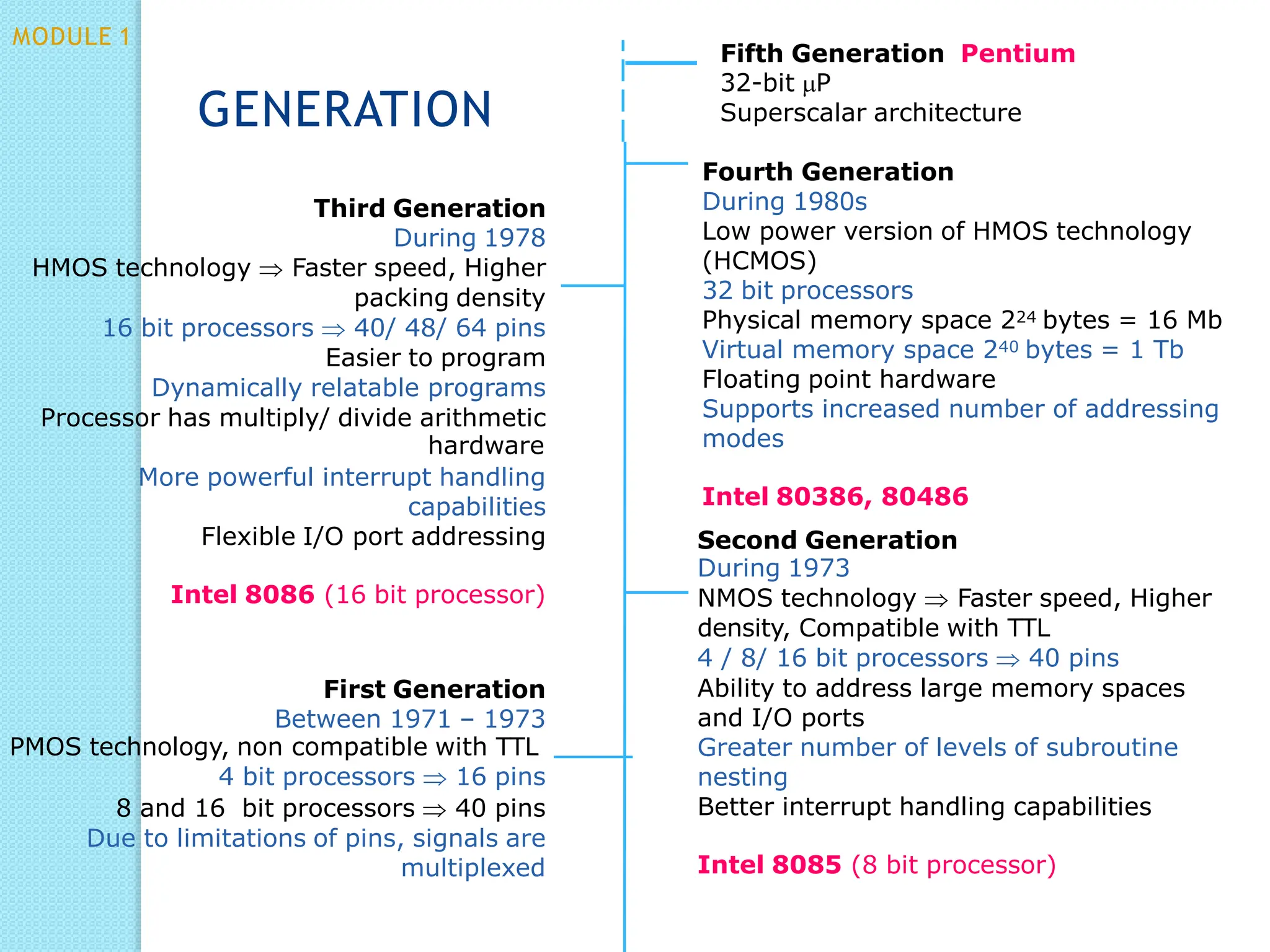
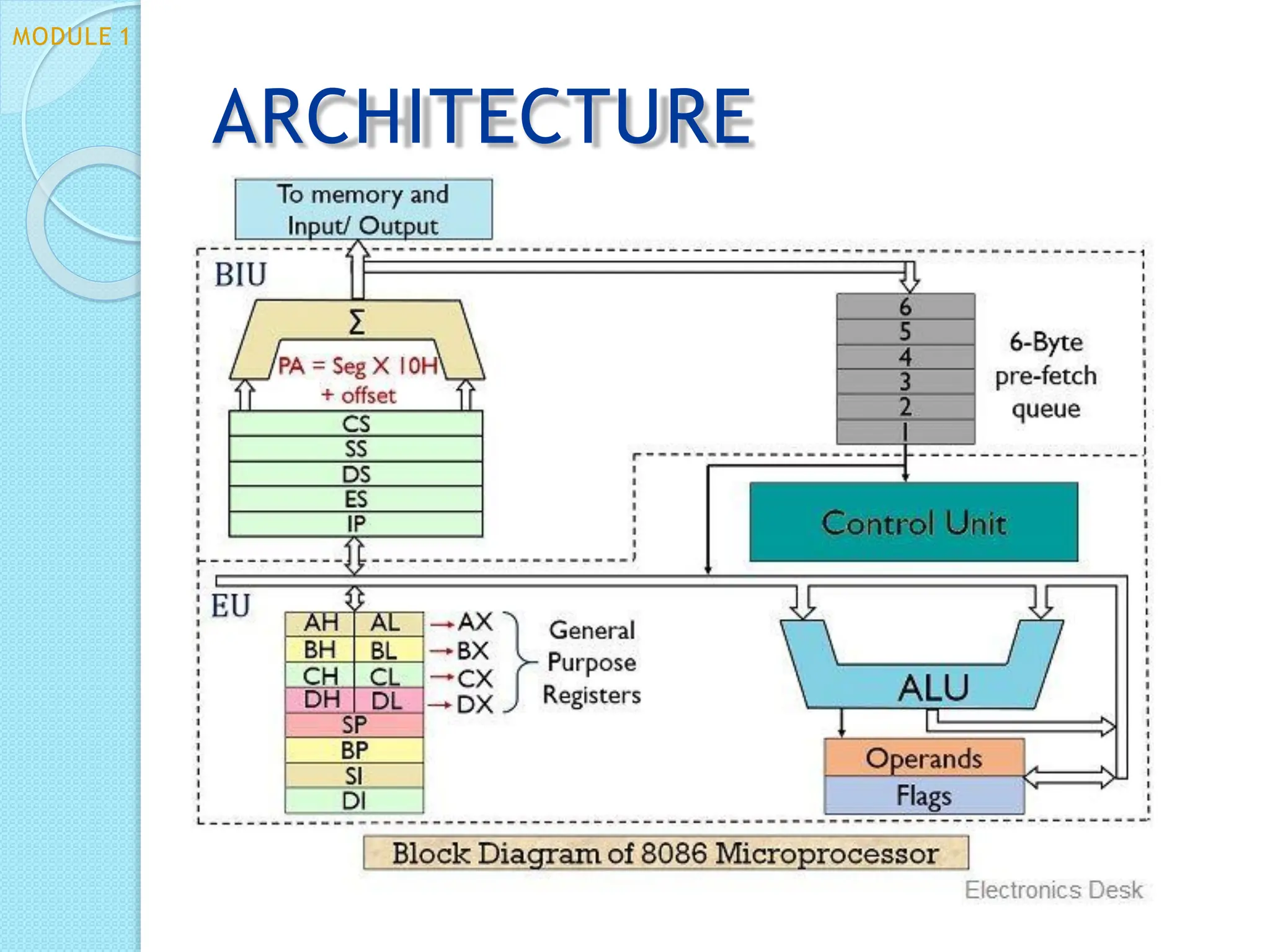
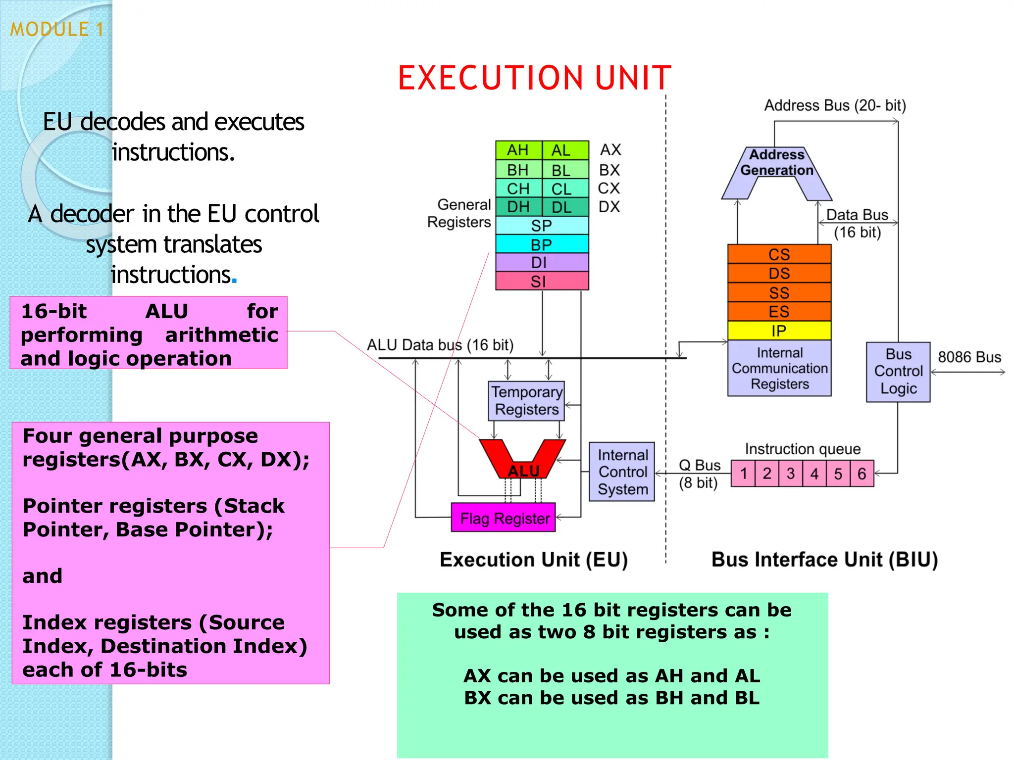
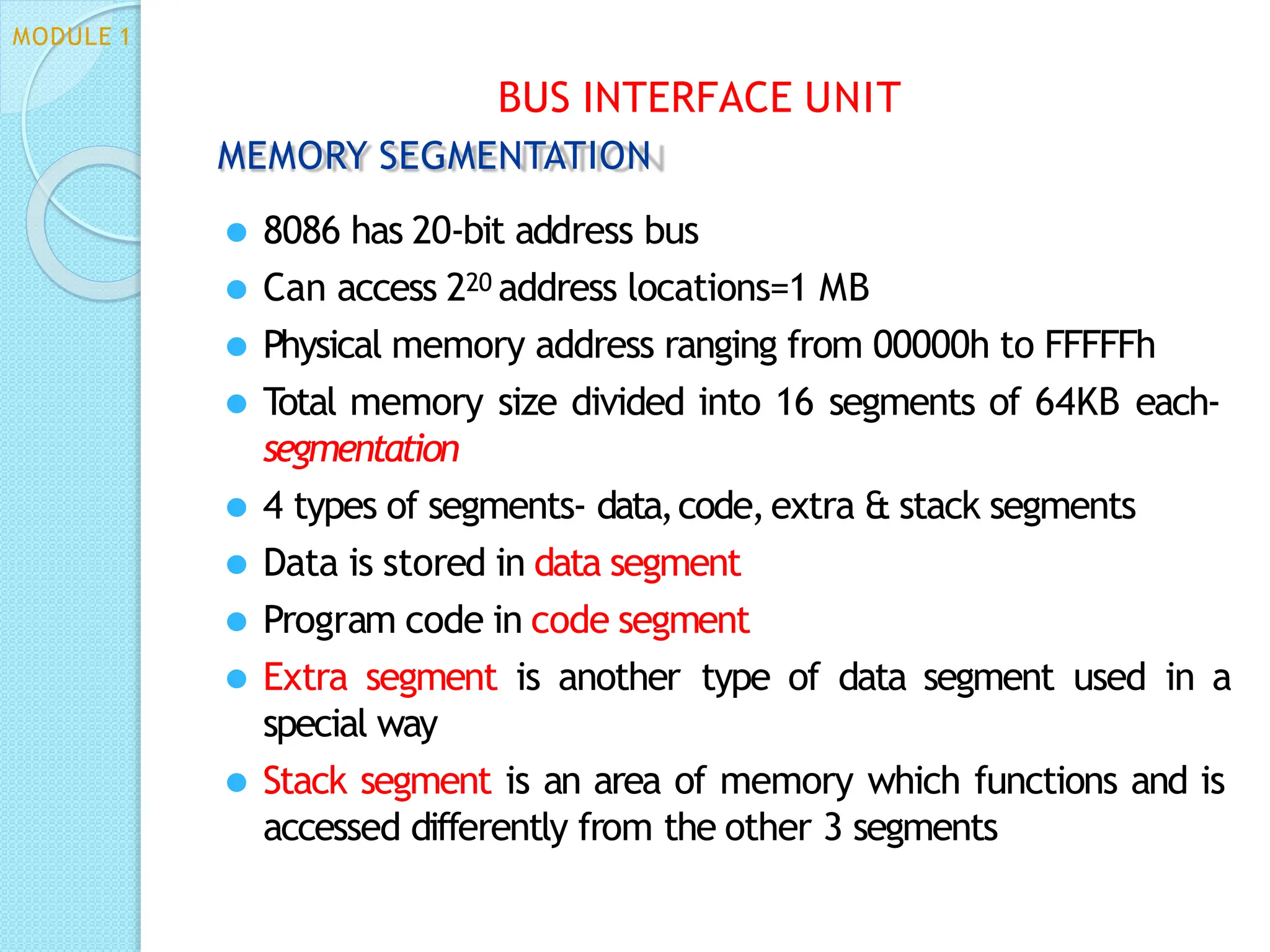
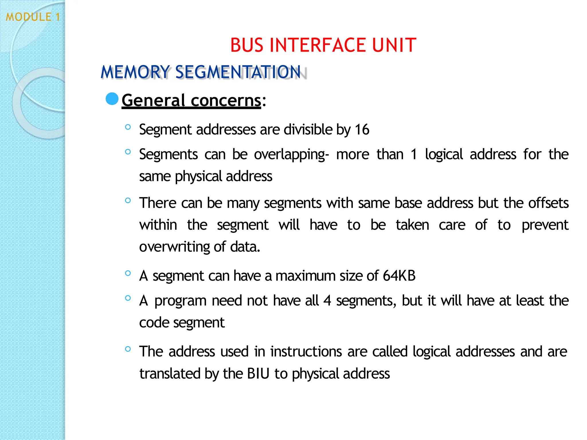
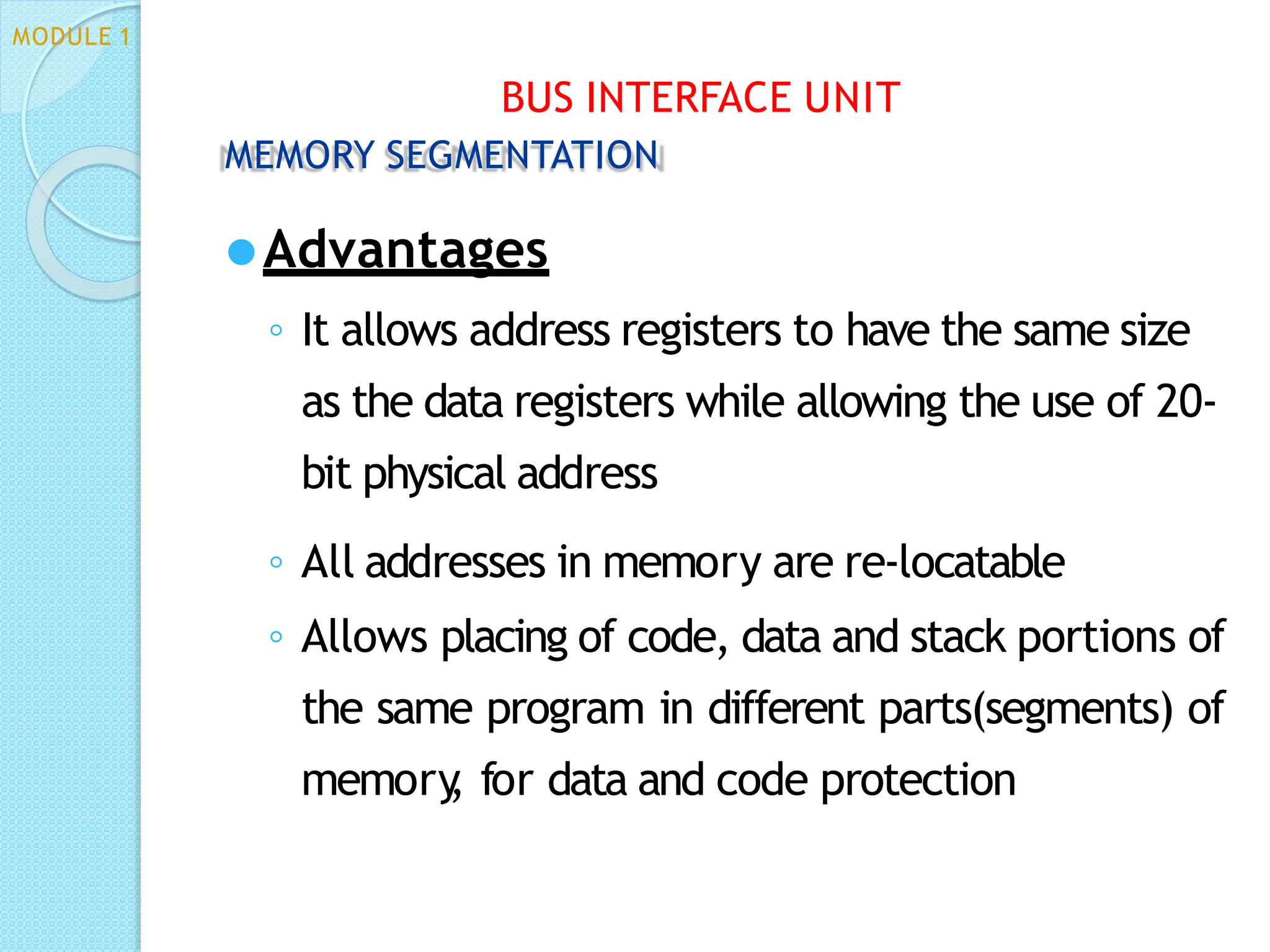
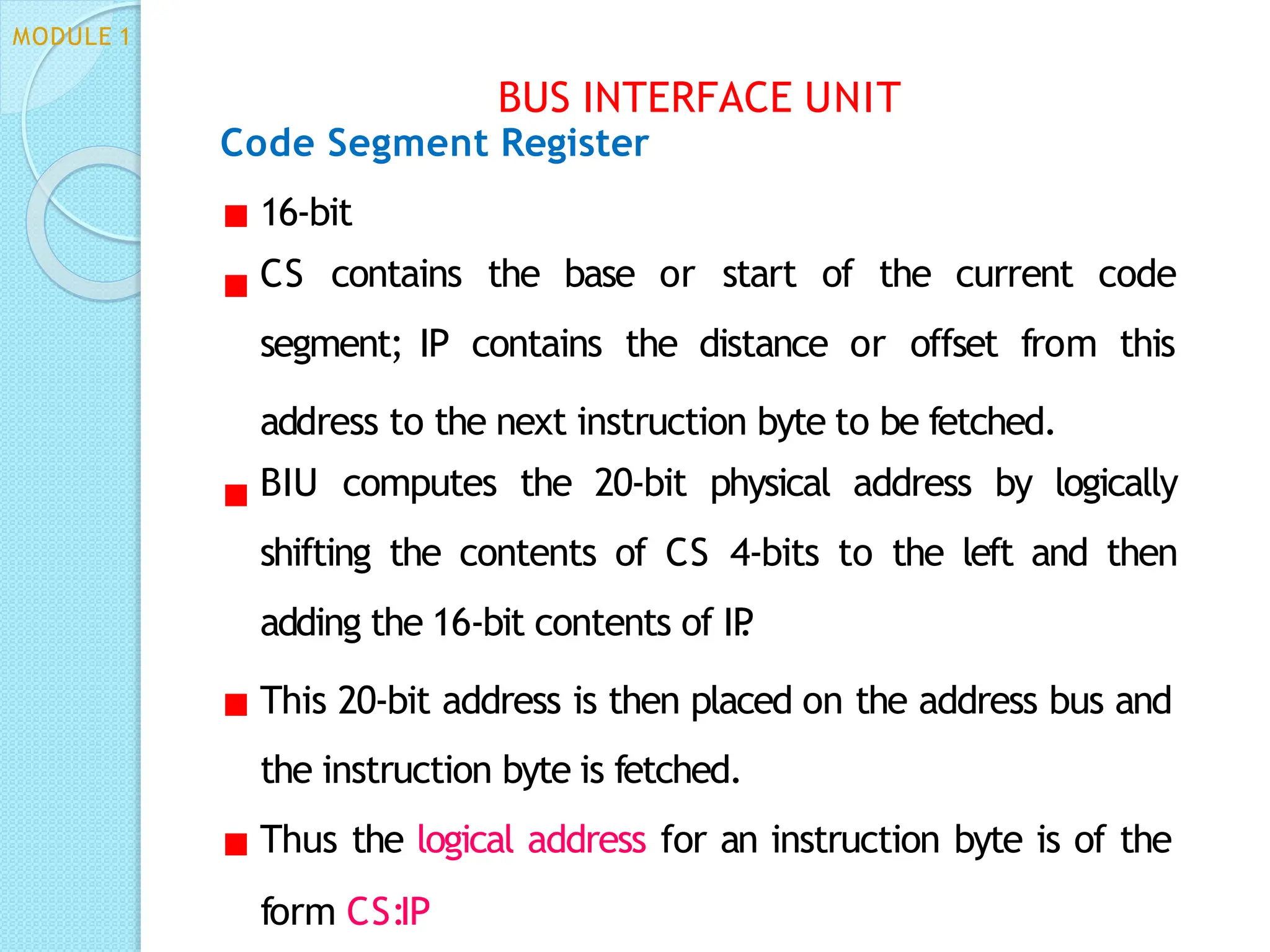
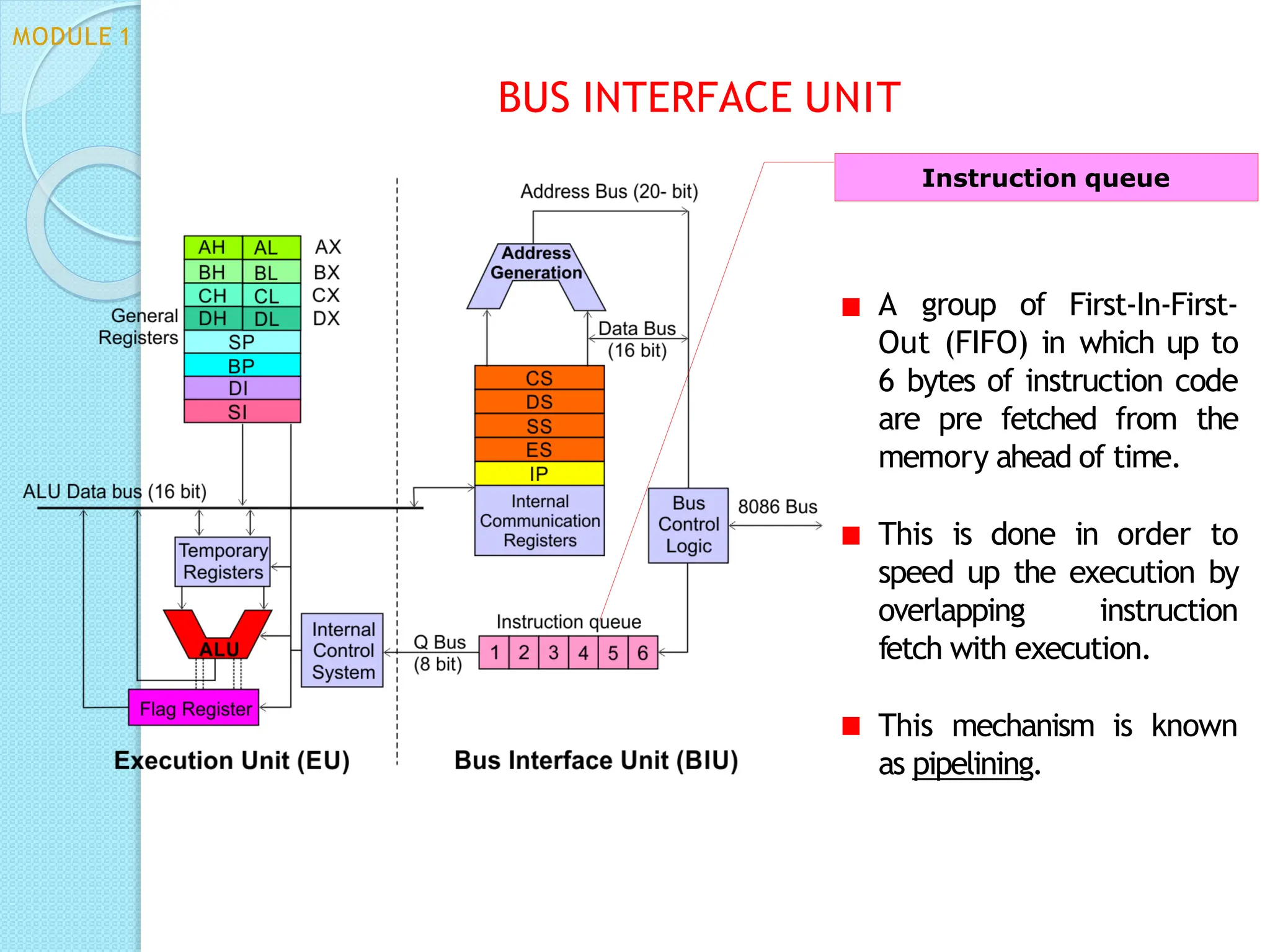
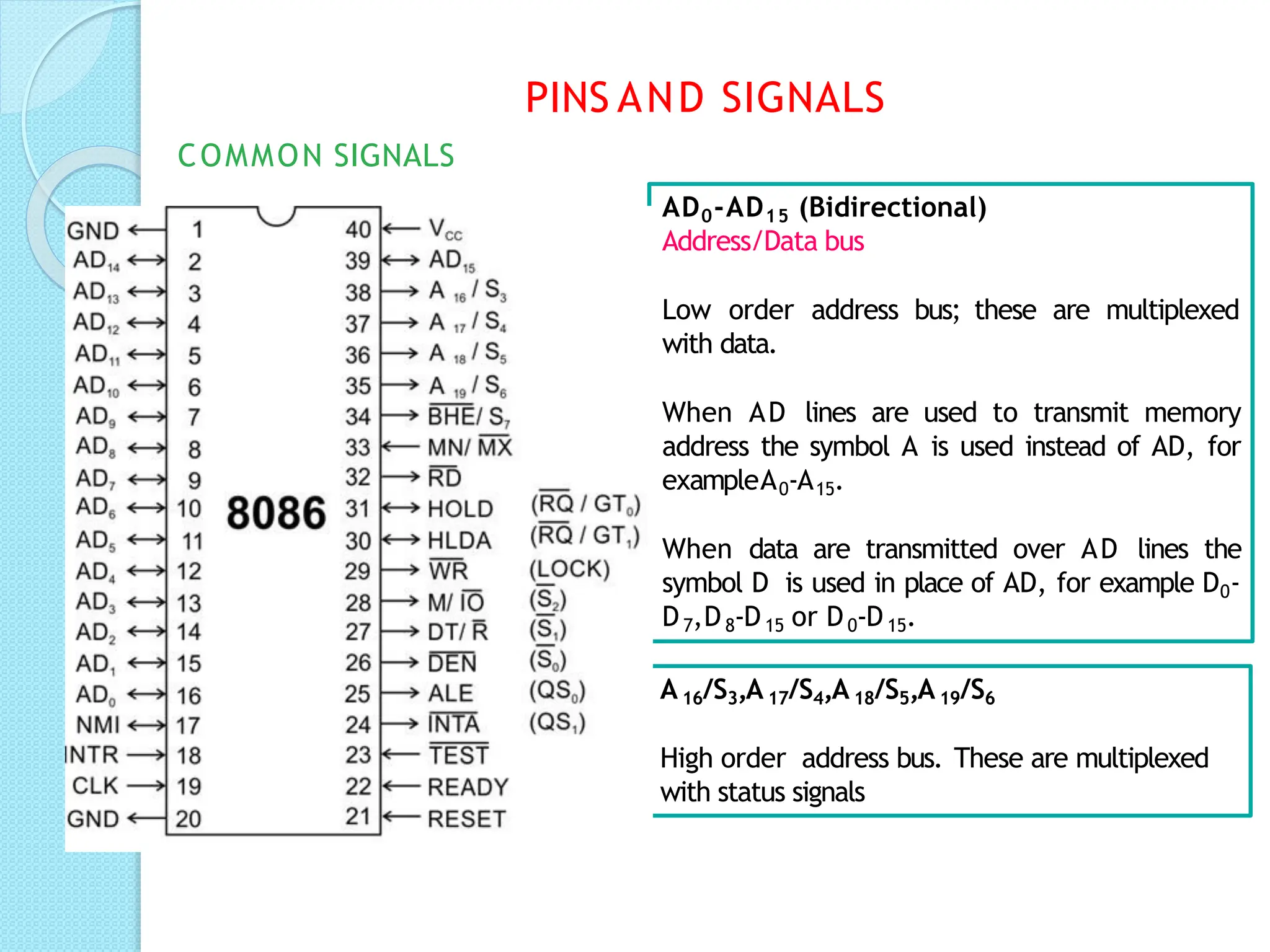
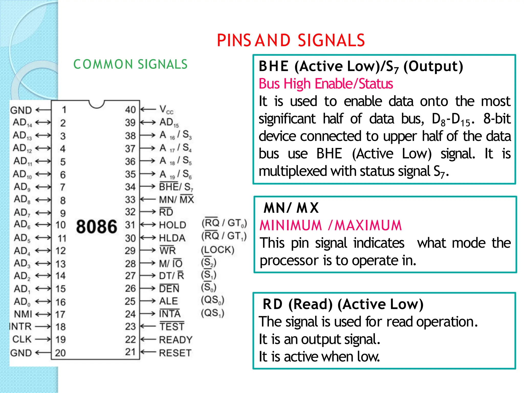
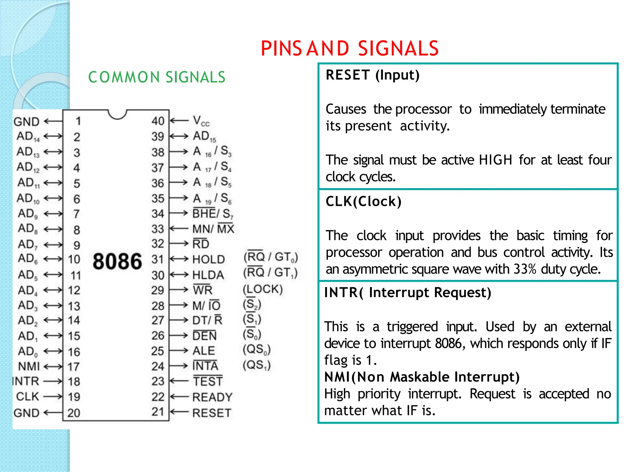
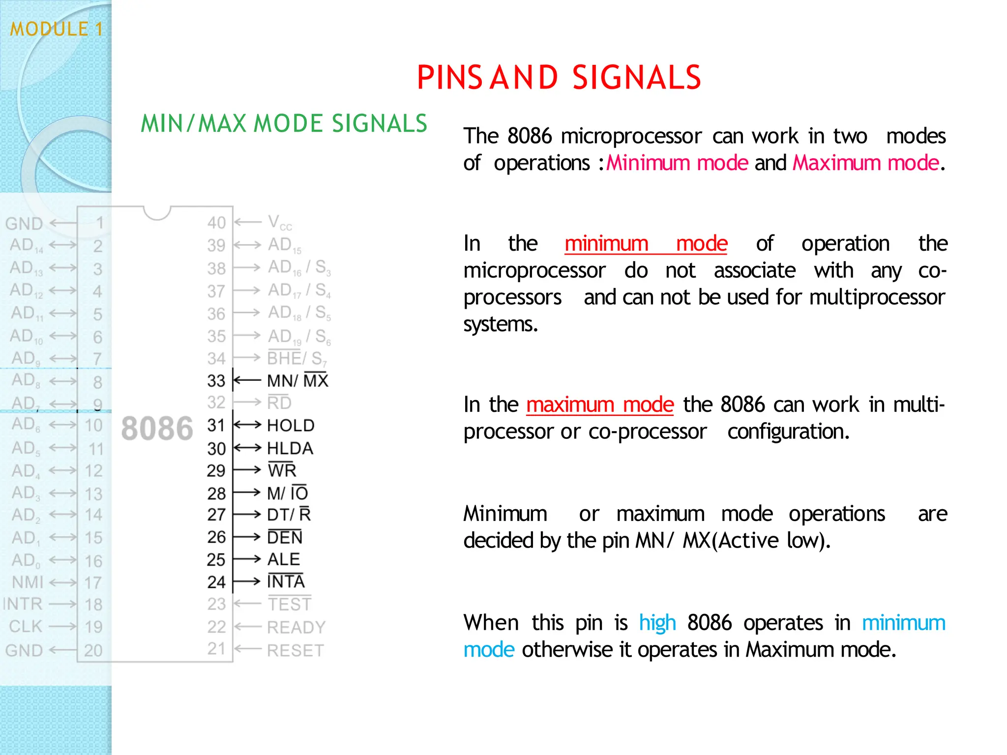
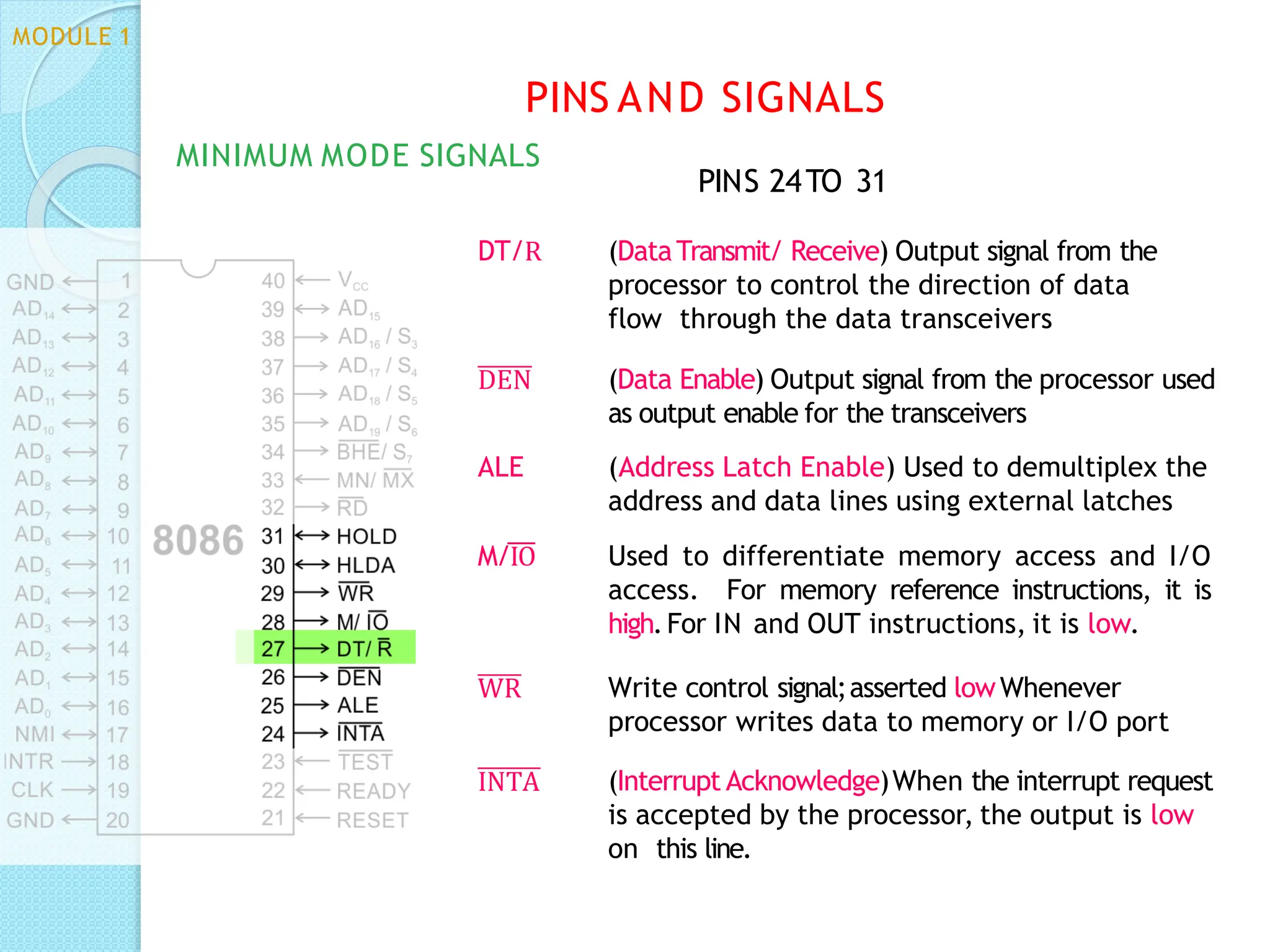
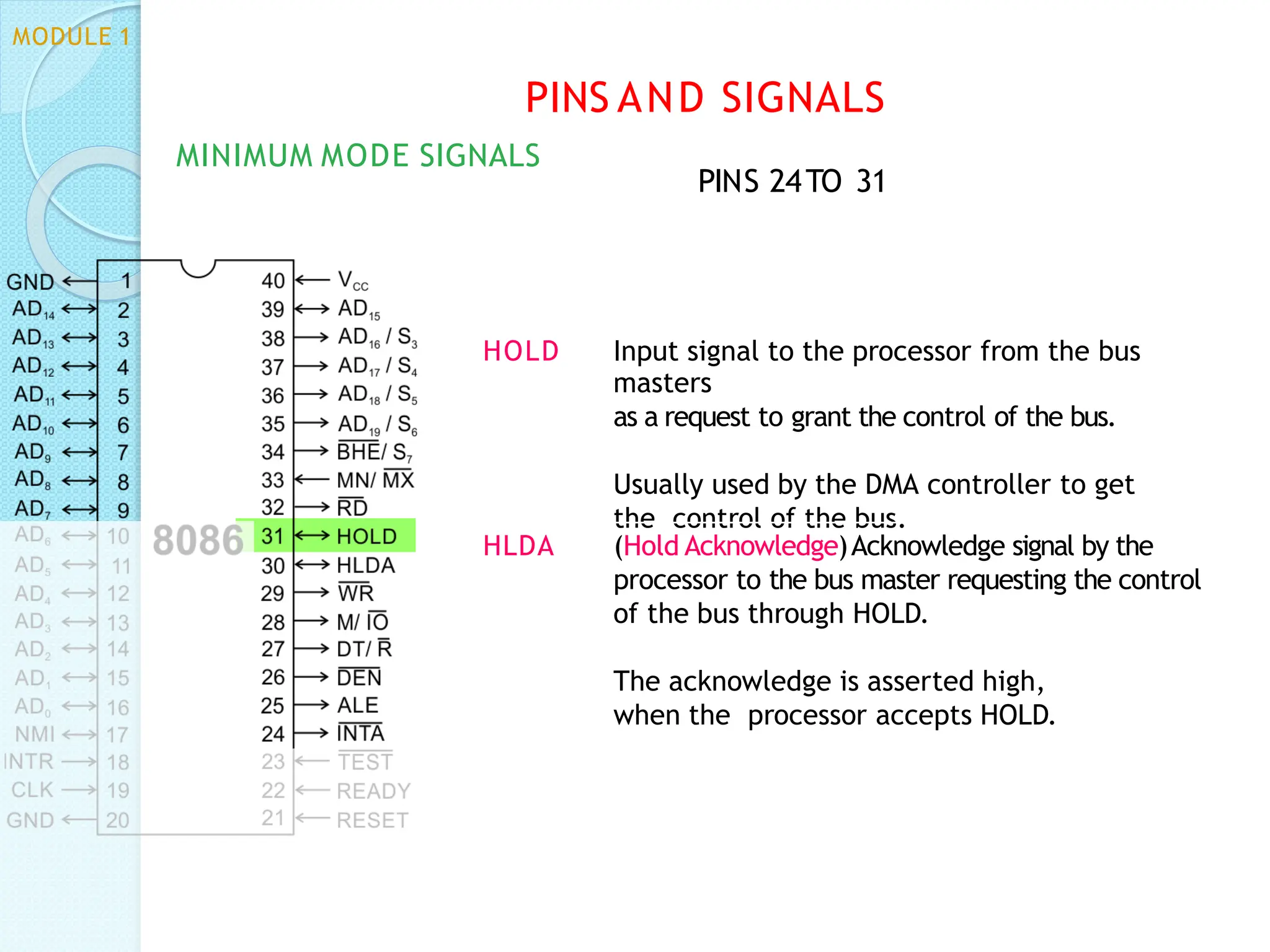
The document provides an extensive overview of the 8086 microprocessor architecture, detailing its memory segmentation, signal descriptions, and addressing modes. It discusses the evolution of microprocessors, the internal architecture of the 8086, including the use of registers, and how the bus interface unit operates. Additionally, it outlines the processor's modes of operation, instruction sets, and specific functionalities of various registers and flags.


![Here, the effective address of the memory
location at which the data operand is stored is
given in the instruction.
The effective address is just a 16-bit number
written directly in the instruction.
Example:
MOV BX, [1354H]
MOV BL, [0400H]
square brackets around the 1354H denotes
The
the contents of the memory location. When
executed, this instruction will copy the contents of
the memory location into BX register.
This addressing mode is called direct because the
displacement of the operand from the segment
base is specified directly in the instruction.
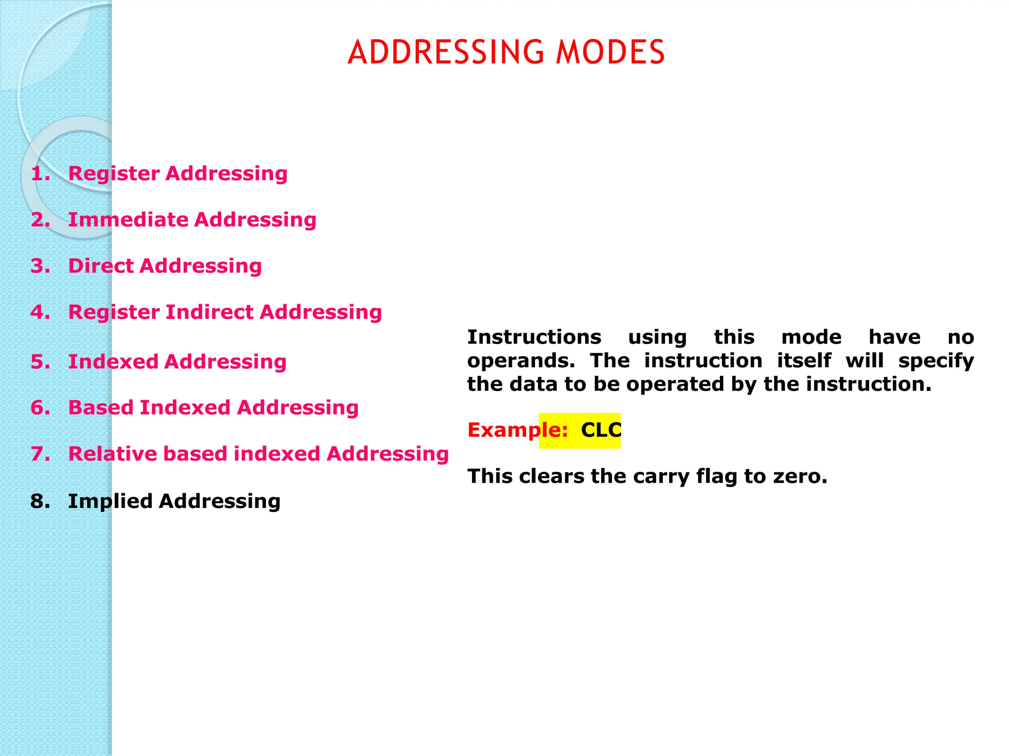
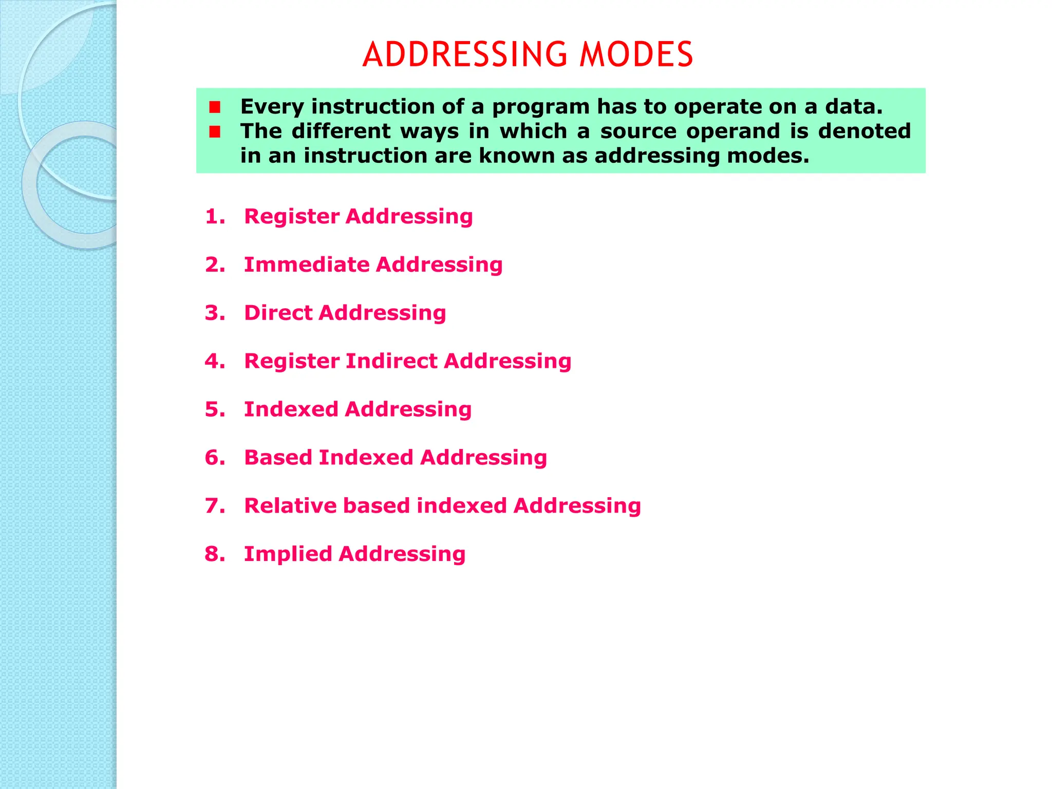
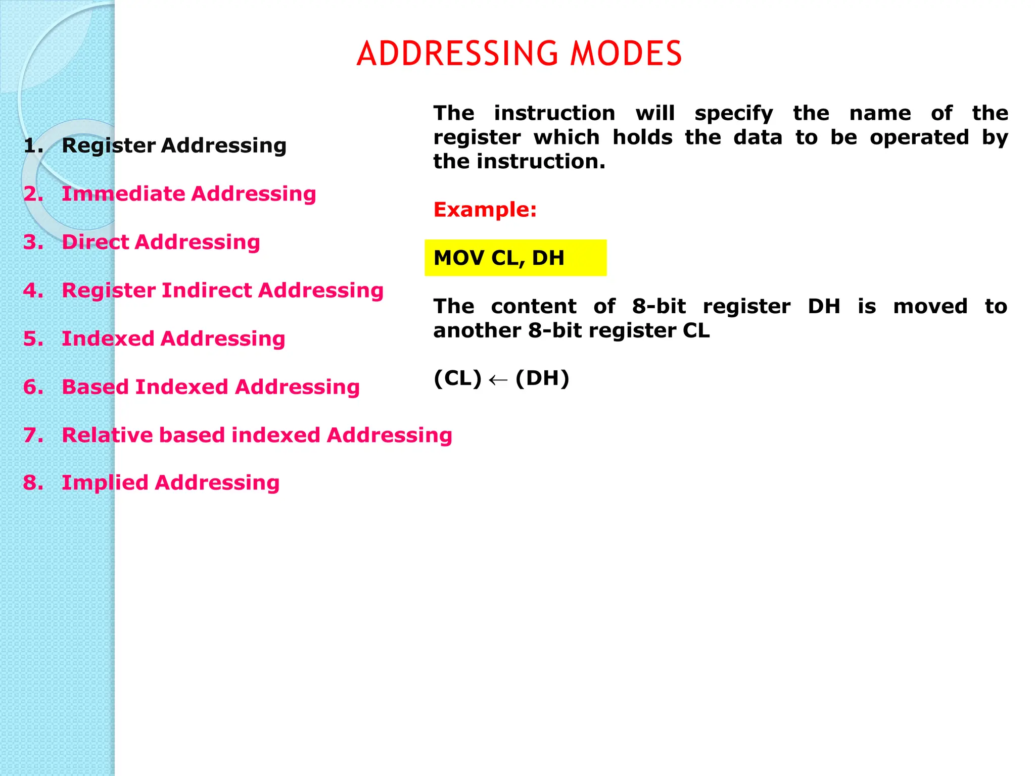
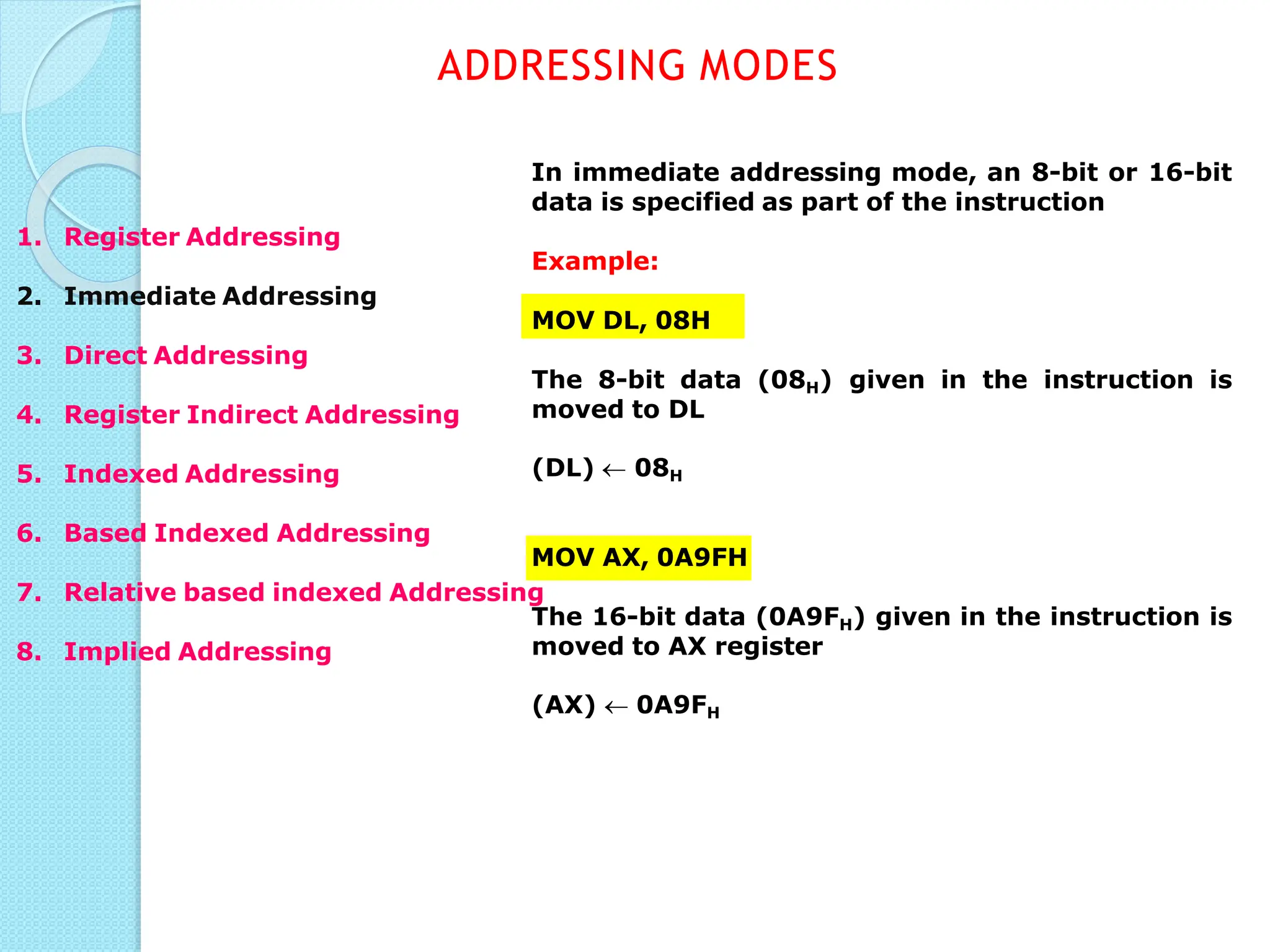
ADDRESSING MODES
1. Register Addressing
2. Immediate Addressing
3. Direct Addressing
4. Register Indirect Addressing
5. Indexed Addressing
6. Based Indexed Addressing
7. Relative based indexed
Addressing
8. Implied Addressing](https://image.slidesharecdn.com/8086architecturepindiagramaddressingmodes3-240729120252-3dc32dc4/75/8086-Architecture-Pin-diagram-Addressing-modes-3-pdf-47-2048.jpg)
![In Register indirect addressing, name of the
register which holds the effective address (EA)
will be specified in the instruction.
Registers used to hold EA are any of the following
registers:
BX, BP, DI and SI.
Content of the DS register is used for base
address calculation.
Example:
MOV CX, [BX]
Operations:
EA = (BX)
BA = (DS) x 1610
MA = BA + EA
(CX) (MA) or,
(CL) (MA)
(CH) (MA +1)
Note : Register/ memory
enclosed in brackets refer to
content of register/ memory
ADDRESSING MODES
1. Register Addressing
2. Immediate Addressing
3. Direct Addressing
4. Register Indirect Addressing
5. Indexed Addressing
6. Based Indexed Addressing
7. Relative based indexed
Addressing
8. Implied Addressing](https://image.slidesharecdn.com/8086architecturepindiagramaddressingmodes3-240729120252-3dc32dc4/75/8086-Architecture-Pin-diagram-Addressing-modes-3-pdf-48-2048.jpg)
![SI or DI register is used to hold an index value for
memory.
In case of 8-bit displacement, it is sign extended
to 16-bit before adding to the base value.
Example:
MOV CX, [SI]
Operations:
offset = (SI)
BA = (DS) x 1610
MA = BA + offset
(CX) (MA) or,
(CL) (MA)
(CH) (MA + 1)
ADDRESSING MODES
1. Register Addressing
2. Immediate Addressing
3. Direct Addressing
4. Register Indirect Addressing
5. Indexed Addressing
6. Based Indexed Addressing
7. Relative based indexed Addressing
8. Implied Addressing](https://image.slidesharecdn.com/8086architecturepindiagramaddressingmodes3-240729120252-3dc32dc4/75/8086-Architecture-Pin-diagram-Addressing-modes-3-pdf-49-2048.jpg)
![In Based Index Addressing, the effective address
is computed from the sum of a base register (BX
or BP) and an index register (SI or DI).
Example:
MOV DX, [BX + SI]
Operations:
000AH 0AH (Sign extended)
EA = (BX) + (SI)
BA = (DS) x 1610
MA = BA + EA
(DL) (MA)
(DH) (MA + 1)
ADDRESSING MODES
1. Register Addressing
2. Immediate Addressing
3. Direct Addressing
4. Register Indirect Addressing
5. Indexed Addressing
6. Based Indexed Addressing
7. Relative based indexed Addressing
(DX) (MA) or,
8. Implied Addressing](https://image.slidesharecdn.com/8086architecturepindiagramaddressingmodes3-240729120252-3dc32dc4/75/8086-Architecture-Pin-diagram-Addressing-modes-3-pdf-50-2048.jpg)
![ADDRESSING MODES
1. Register Addressing
2. Immediate Addressing
3. Direct Addressing
4. Register Indirect Addressing
5. Indexed Addressing
6. Based Indexed Addressing
7. Relative based indexed Addressing
8. Implied Addressing
In relative based Indexed Addressing, the
effective address is computed from the sum of a
base register (BX or BP), an index register (SI or
DI) and a displacement.
Example:
MOV DX, [BX + SI + 0AH]
Operations:
000AH 0AH (Sign extended)
EA = (BX) + (SI) + 000AH
BA = (DS) x 1610
MA = BA + EA
(DX) (MA) or,
(DL) (MA)
(DH) (MA + 1)](https://image.slidesharecdn.com/8086architecturepindiagramaddressingmodes3-240729120252-3dc32dc4/75/8086-Architecture-Pin-diagram-Addressing-modes-3-pdf-51-2048.jpg)