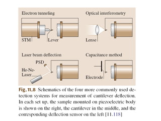
1. The document discusses atomic force microscopy (AFM) and scanning tunneling microscopy (STM), which allow visualization of surfaces at the atomic scale. AFM works by measuring the deflection of a cantilever with a sharp tip as it is moved over a sample surface, detecting atomic-scale surface features.
2. The history of AFM and STM is summarized, including their invention in the 1980s. AFM can image both conducting and insulating surfaces, while STM requires a conductive surface. Contact and non-contact AFM modes are described.
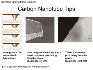
3. Fabrication of AFM tips is discussed, including the use of carbon nanotubes which can achieve higher resolution. Specific applications of A