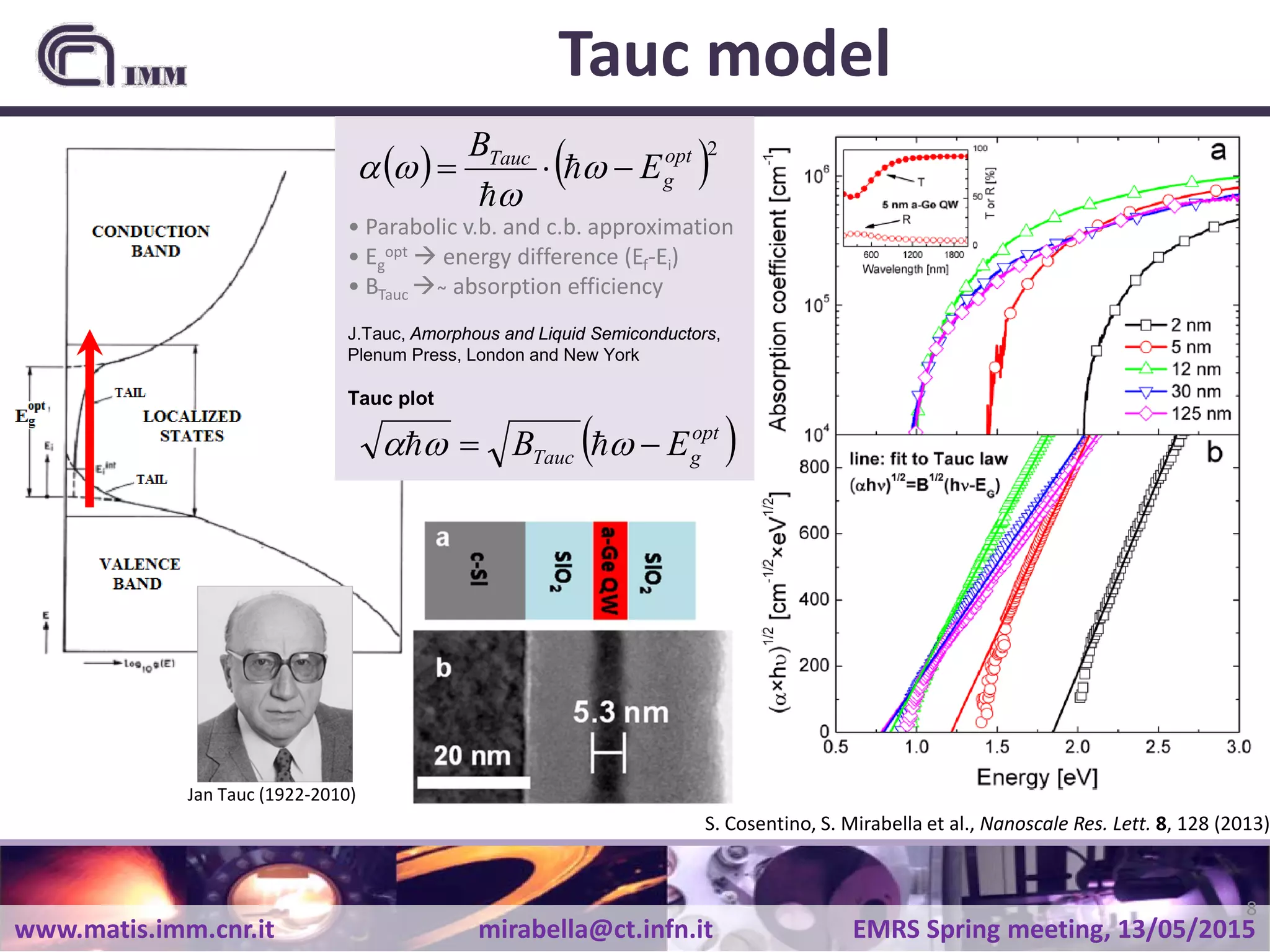
Download as PDF, PPTX
![www.matis.imm.cnr.it mirabella@ct.infn.it EMRS Spring meeting, 13/05/2015
Cullis et al. - J. Appl. Phys., 82, 909 (1997)
Park et al., Phys. Rev. Lett. 86, 1355 (2001)
E. Barbagiovanni et al. - J. Appl. Phys., 111, 034307 (2012)
5 10 15
0.5
1.0
1.5
2.0
2.5
3.0
Energygap[eV]
Size [nm]
Si QD in SiO2
Si QWin SiO2
Ge QD in SiO2
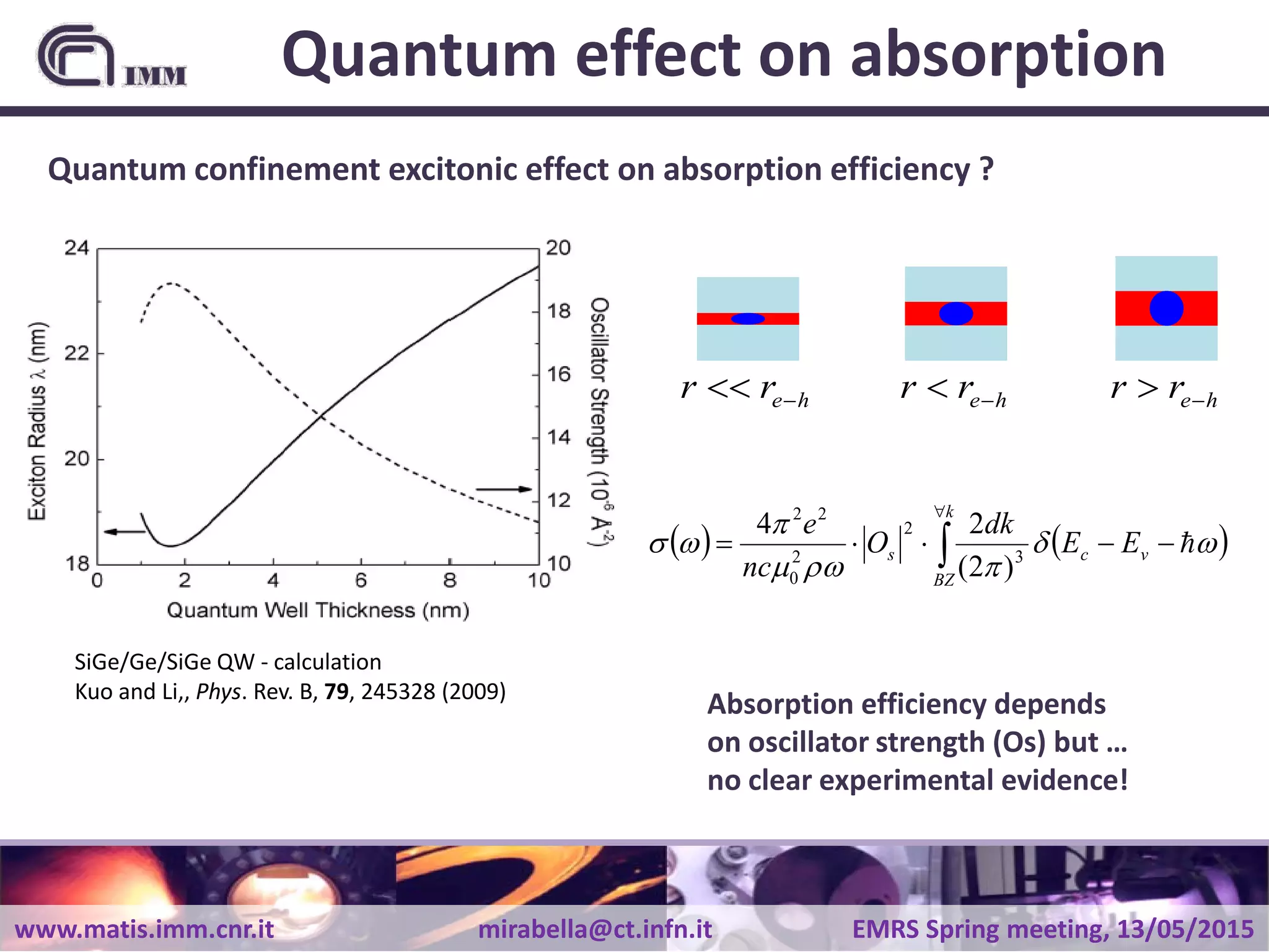
The quantum chance
F. Priolo et al., Nature Nanotechnology 9, 19 (2014)
( ) 2*
22
2
)(
Lm
bulkENSE gg
π
+=
Si
SiO2](https://image.slidesharecdn.com/mirabellaemrs15-sympc2-150512221705-lva1-app6892/75/Light-absorption-enhancement-in-extremely-confined-Ge-nanostructures-2-2048.jpg)
![www.matis.imm.cnr.it mirabella@ct.infn.it EMRS Spring meeting, 13/05/2015
Ge versus Si QDs
1 2 3 4 5
103
104
105
106
Absorptioncoefficient[cm-1
]
Energy [eV]
Silicon
Germanium
Si QDs
Ge QDs
• Higher absorption coefficient
• Larger size range for QCE
• Bandgap tuning within solar spectrum](https://image.slidesharecdn.com/mirabellaemrs15-sympc2-150512221705-lva1-app6892/75/Light-absorption-enhancement-in-extremely-confined-Ge-nanostructures-3-2048.jpg)
![www.matis.imm.cnr.it mirabella@ct.infn.it EMRS Spring meeting, 13/05/2015
Quantum effect on Eg
E. Barbagiovanni et al. J. Appl.
Phys., 111, 034307 (2012)
( ) 2*
22
2
)(
Lm
bulkENSE gg
π
+=Quantum confinement effect: does only size matter ?
Optical bandgap depends on several factors:
how to model the QCE on Eg ?
other effects on absorption ?
0 200 400 600 800 1000 1200
2,1
2,4
2,7
3,0
MSsamples:
43-S
46-S
PECVDsamples:
43-C
46-C
46-SL
EOPT
g
[eV]
Temperature [°C]
Si QDs
S. Mirabella et al. J. Appl.
Phys., 106, 103505 (2009)
Si QDs - calculation
P. Hapala et al., Phys. Rev. B,
87, 195420 (2013)](https://image.slidesharecdn.com/mirabellaemrs15-sympc2-150512221705-lva1-app6892/75/Light-absorption-enhancement-in-extremely-confined-Ge-nanostructures-4-2048.jpg)
![www.matis.imm.cnr.it mirabella@ct.infn.it EMRS Spring meeting, 13/05/2015
Single Ge quantum well
0.8
1.0
1.2
1.4
1.6
1.8
2.0
0 5 10 15 20 25 30 125
4
8
12
16
20
B[×10-1
(eV×nm)-1
]
(b)
(a)
Energygap[eV]
EG
Fit, Eg
=Eg-Bulk
+A/L2
A= 4.35 [eV×nm2
]
OS
[×10-4
nm-2
]
Quantum well thickness [nm]
OS
in Ge QW (theory, Kuo PRB2009)
0.3
0.6
0.9
1.2
1.5
B (measured)
Tauc approach to extract in Ge NS:
- optical bandgap (Eg)
- absorption efficiency (BTauc)
BTauc is proportional to
the oscillator strength
S. Cosentino, S. Mirabella et al., Nanoscale Res. Lett. 8, 128 (2013)](https://image.slidesharecdn.com/mirabellaemrs15-sympc2-150512221705-lva1-app6892/75/Light-absorption-enhancement-in-extremely-confined-Ge-nanostructures-9-2048.jpg)
![www.matis.imm.cnr.it mirabella@ct.infn.it EMRS Spring meeting, 13/05/2015
Ge QDs synthesis
SiGeO film
PECVD or sputter
(deposition 250°C: 8 - 20% Ge)
(600-800°C annealing in N2)
Ge QDs (2-8 nm) embedded in SiO2
5.0x10²¹
1.0x10²²
1.5x10²²
0
2
4
6
8
10
PECVD
sputter
QDsize[nm]
Ge concentration [cm-3
]](https://image.slidesharecdn.com/mirabellaemrs15-sympc2-150512221705-lva1-app6892/75/Light-absorption-enhancement-in-extremely-confined-Ge-nanostructures-11-2048.jpg)
![www.matis.imm.cnr.it mirabella@ct.infn.it EMRS Spring meeting, 13/05/2015
RBS
sigeo90_asdep_ran(x2y7).RBS
Simulated
Channel
600550500450400350300250200
Counts
2.000
1.900
1.800
1.700
1.600
1.500
1.400
1.300
1.200
1.100
1.000
900
800
700
600
500
400
300
200
100
0
600 700 800 900 1000 1100 1200 1300 1400 1500 1600
Energy [keV]
Si
SiGeO
2 MeV
He+
O
Si
Ge
• Ge QDs density (~ 1018 cm-3) and spacing (1-3 nm)
• Light absorption analysis
5.0x10²¹
1.0x10²²
1.5x10²²
0
1
2
3
4
PECVD
sputter
QD-QDdistance[nm]
Ge concentration [cm-3
]](https://image.slidesharecdn.com/mirabellaemrs15-sympc2-150512221705-lva1-app6892/75/Light-absorption-enhancement-in-extremely-confined-Ge-nanostructures-12-2048.jpg)
![www.matis.imm.cnr.it mirabella@ct.infn.it EMRS Spring meeting, 13/05/2015
Light absorption cross section
absorption (α) absorption cross section (σ): photon absorption probability per Ge dose
D
t
ασ =
• Red shift with decreasing QD size
• Greater shift in PECVD w.r.t. sputter
1 2 3 4 5
10-19
10-18
10-17
PECVD QDs (3.5 nm)
PECVD QDs (4.4 nm)
Sputter QDs (3 nm)
Sputter QDs (4 nm)
Absorptioncrosssection[cm2
]
Energy [eV]](https://image.slidesharecdn.com/mirabellaemrs15-sympc2-150512221705-lva1-app6892/75/Light-absorption-enhancement-in-extremely-confined-Ge-nanostructures-13-2048.jpg)
![www.matis.imm.cnr.it mirabella@ct.infn.it EMRS Spring meeting, 13/05/2015
Optical bandgap variation
2 4 6 8 10
1.0
1.5
2.0
2.5
3.0
QD size [nm]
PECVD
Sputter
a-Ge bulk
OpticalBandgap[eV]
2 4 6 8 10
1.0
1.5
2.0
2.5
3.0
QD size [nm]
PECVD
Sputter
a-Ge bulk
EMA
OpticalBandgap[eV]
• Eg modulation is dependent on synthesis technique
( ) 2*
22
2
)(
Lm
bulkENSE gg
π
+=
QD
Is the interface
playing a role ?
• Why different Eg
modulation ?
• How to model the QCE ?
• Eg modulation is dependent on synthesis technique
• EMA cannot account for none of the two](https://image.slidesharecdn.com/mirabellaemrs15-sympc2-150512221705-lva1-app6892/75/Light-absorption-enhancement-in-extremely-confined-Ge-nanostructures-14-2048.jpg)
![www.matis.imm.cnr.it mirabella@ct.infn.it EMRS Spring meeting, 13/05/2015
EELS-STEM analysis
2 nm
• Chemical analysis of QD surrounding
• Different oxide contribution
0.2
0.4
0.6
0.8
1.0
5 10 15 20 25 30 35 40 45 50 55 60
0.2
0.4
0.6
0.8
1.0
GeO
SiO2
PECVD
Intensity[a.u.]
Core
Interface
Matrix
Sputter
Ge
Intensity[a.u.]
Energy [eV]
5 nm QD
5 nm QD
JEOL ARM200CF
www.beyondnano.it
Probe size:
0.2x0.2 nm](https://image.slidesharecdn.com/mirabellaemrs15-sympc2-150512221705-lva1-app6892/75/Light-absorption-enhancement-in-extremely-confined-Ge-nanostructures-16-2048.jpg)
![www.matis.imm.cnr.it mirabella@ct.infn.it EMRS Spring meeting, 13/05/2015
EELS-STEM analysis
0.0
0.2
0.4
0.6
0.8
1.0
5 10 15 20 25 30 35 40 45 50 55 60
0.0
0.2
0.4
0.6
0.8
1.0
Sputter
Intensity[a.u.]
PECVD
Intensity[a.u.]
Energy [eV]
EELScore QD
Fit
interband transition Ge
Ge QDvol. plasmon
SiO2
vol. plasmon
Ge-Ge M4,5
band
Ge-OM4,5
band
AGe-O
AGe-Ge
AGe-pl )( plGeGeGe
OGe
OGe
AA
A
F
−−
−
−
+
=
FGe-O ~ 16 % for sputter
FGe-O ~ 8 % for PECVD
S. Cosentino, S. Mirabella et al., Nanoscale (2015) submitted
STEM: e-beam probe a
cylinder of ~ 40 Ge atoms,
3 of which at surfaces
• Significant Ge-O surface contribution
• Greater Ge-O contribution in sputter samples
e-beam](https://image.slidesharecdn.com/mirabellaemrs15-sympc2-150512221705-lva1-app6892/75/Light-absorption-enhancement-in-extremely-confined-Ge-nanostructures-17-2048.jpg)
![www.matis.imm.cnr.it mirabella@ct.infn.it EMRS Spring meeting, 13/05/2015
Interface effect on bandgap
2 4 6 8 10
1.0
1.5
2.0
2.5
3.0
QD size [nm]
PECVD
Sputter
a-Ge bulk
OpticalBandgap[eV]
2 4 6 8 10
1.0
1.5
2.0
2.5
3.0
QD size [nm]
PECVD
Sputter
a-Ge bulk
EMA
OpticalBandgap[eV]
2 4 6 8 10
1.0
1.5
2.0
2.5
3.0
QD size [nm]
PECVD
Sputter
a-Ge bulk
EMA
SPDEMPECVD
SPDEMSputter
OpticalBandgap[eV]
E. G. Barbagiovanni, et al., J. Appl. Phys. (2012), 111, 034307
E. G. Barbagiovanni, et al. Physica E, (2014), 63, 14–20
E. G. Barbagiovanni, S. Mirabella et al., J. Appl. Phys. (2015) accepted
S. Cosentino, S. Mirabella et al., Nanoscale (2015) submitted
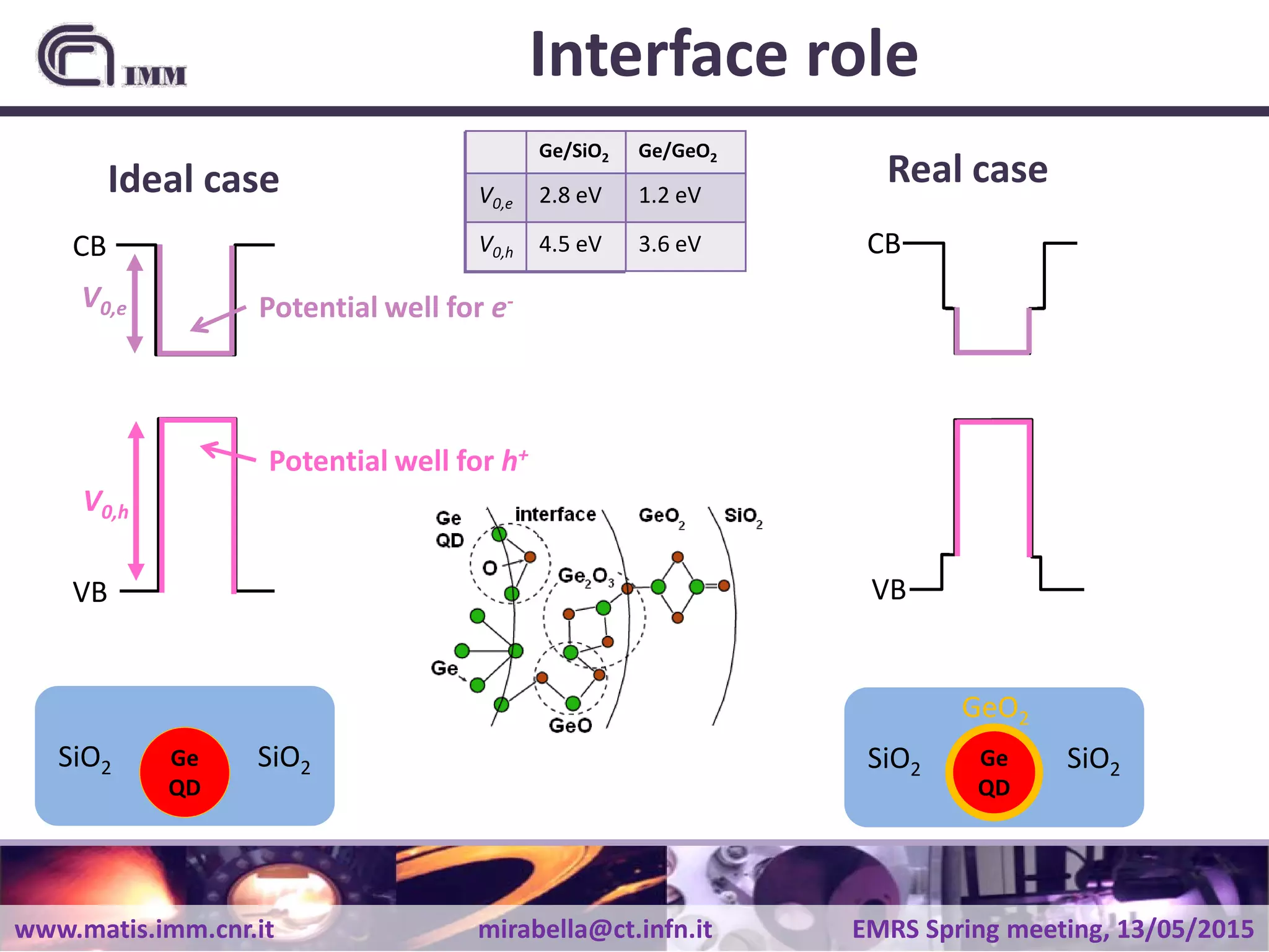
Ge/SiO2 Ge/GeO2 PECVD Sputter
V0,e 2.8 eV 1.2 eV 1.1 eV 0.9 eV
V0,h 4.5 eV 3.6 eV 3.3 eV 2.8 eV
( )
( )
+
⋅
+= *
,
,
*
,
,
2
3
hc
hc
ec
ecbulk
gg
m
V
m
V
DD
EDE
µ
SPDEM model well accounts
for the Eg variation](https://image.slidesharecdn.com/mirabellaemrs15-sympc2-150512221705-lva1-app6892/75/Light-absorption-enhancement-in-extremely-confined-Ge-nanostructures-19-2048.jpg)
![www.matis.imm.cnr.it mirabella@ct.infn.it EMRS Spring meeting, 13/05/2015Paper of Eric on arxiv?
Interface effects
S. Cosentino, S. Mirabella et al., Nanoscale (2015) submitted
• GeO2 act as the confining potential
• A thinner and GeO poor interface
gives larger QCE
• … what about absorption efficiency ?
2 4 6 8 10
5.0x10⁻¹⁸
1.0x10⁻¹⁷
1.5x10⁻¹⁷
Absorption Efficiency
Ge QDs PECVD
Ge QDs Sputter
B*
Tauc
[eV-1
×cm2
]
QD size [nm]
2X increase
Light absorption in Ge quantum dots in SiO2](https://image.slidesharecdn.com/mirabellaemrs15-sympc2-150512221705-lva1-app6892/75/Light-absorption-enhancement-in-extremely-confined-Ge-nanostructures-20-2048.jpg)
![www.matis.imm.cnr.it mirabella@ct.infn.it EMRS Spring meeting, 13/05/2015
Multilayer approach
Sample
t
[nm]
d
[nm]
N
ML-2 2 20 15
ML-4 4.5 20 4
SL-330 330 - 1
Multilayer approach for:
• narrowing size distribution (Zacharias APL2002)
• increasing average distance among QDs
Fixed SiO2 barrier thickness: 20 nm
N SiGeO layers, from 4 to 15
Comparison with a single layer (330 nm)
d: SiO2 barrier
t: SiGeO layer](https://image.slidesharecdn.com/mirabellaemrs15-sympc2-150512221705-lva1-app6892/75/Light-absorption-enhancement-in-extremely-confined-Ge-nanostructures-22-2048.jpg)
![www.matis.imm.cnr.it mirabella@ct.infn.it EMRS Spring meeting, 13/05/2015
Absorption coefficient
1 2 3 4 5 6
103
104
105
106
Absorptioncoefficient[cm-1
]
Energy[eV]
c-Ge bulk
SL-330
1 2 3 4 5 6
103
104
105
106
Absorptioncoefficient[cm-1
]
Energy[eV]
c-Ge bulk
SL-330
ML-2
ML-4
• Multilayered samples show similar
absorption onset to single layer
• … but much higher absorption efficiency!](https://image.slidesharecdn.com/mirabellaemrs15-sympc2-150512221705-lva1-app6892/75/Light-absorption-enhancement-in-extremely-confined-Ge-nanostructures-23-2048.jpg)
![www.matis.imm.cnr.it mirabella@ct.infn.it EMRS Spring meeting, 13/05/2015
RBS and TEM analysis
Sample
t
[nm]
d
[nm]
N
Ge % in
SiGeO
QD
size
ML-2 2 20 15 10.6 2
ML-4 4.5 20 4 8.9 1.7
SL-330 330 - 1 10.0 2.9
450 500 550
0
50
100
150
200
250
300
He+
backscattered
from Ge atoms
RBSyield[counts]
Channel
ML-2
ML-4
2 MeV He+
beam
165° backscattering angle](https://image.slidesharecdn.com/mirabellaemrs15-sympc2-150512221705-lva1-app6892/75/Light-absorption-enhancement-in-extremely-confined-Ge-nanostructures-24-2048.jpg)
![www.matis.imm.cnr.it mirabella@ct.infn.it EMRS Spring meeting, 13/05/2015
Light absorption Ge QD in MLs
10-17
10-16
σ[cm2
]
2 3 4 5 6
0
1
2
ML-2
ML-4
SL-330
(σhν)1/2
[10-9
cmxeV1/2
]
Energy[eV]
• Similar optical bandgap
• Strong increase of absorption efficiency
• Independent modulation of Eg and B*
• ML configuration allows for absorption
increase
10 X increase!
Same Eg
R. Raciti et al.
Poster CP2 #44
Today 14-16](https://image.slidesharecdn.com/mirabellaemrs15-sympc2-150512221705-lva1-app6892/75/Light-absorption-enhancement-in-extremely-confined-Ge-nanostructures-25-2048.jpg)
![www.matis.imm.cnr.it mirabella@ct.infn.it EMRS Spring meeting, 13/05/2015
Multiple screening effect
Si QDs - ε2 calculation in one Si QD
R. Guerra et al., Phys. Rev. B, 84, 075342 (2011)
Local Field Effects
Lower screening of e.m. radiation by
induced polarization (local field effects)
2 4 6 8 10
0.0
5.0x10⁻¹⁷
1.0x10⁻¹⁶
1.5x10⁻¹⁶
PECVD
Sputter
ML-PECVD
Ge bulk
BTauc
[eV-1
×cm2
]
QD size [nm]
15X increase](https://image.slidesharecdn.com/mirabellaemrs15-sympc2-150512221705-lva1-app6892/75/Light-absorption-enhancement-in-extremely-confined-Ge-nanostructures-26-2048.jpg)
![www.matis.imm.cnr.it mirabella@ct.infn.it EMRS Spring meeting, 13/05/2015
CONCLUSIONS
Based on:
S. Mirabella et al. JAP 106, 103505 (2009)
E. Barbagiovanni et al. JAP 111, 034307 (2012)
S. Cosentino et al. NRL 8, 128 (2013)
S. Mirabella et al. APL 102, 193105 (2013)
E. Barbagiovanni et al. PE 63, 14 (2014)
S. Cosentino et al. JAP 115, 043103 (2014)
S. Cosentino et al. SOLMAT 135, 22 (2015)
E. Barbagiovanni et al. JAP (2015) accepted
S. Cosentino et al. Nanoscale (2015) submitted
SiO2 SiO2Ge
QD
GeO2
2 4 6 8 10
1.0
1.5
2.0
2.5
3.0
QD size [nm]
PECVD
Sputter
a-Ge bulk
EMA
SPDEMPECVD
SPDEMSputter
OpticalBandgap[eV]
2 3 4 5 6
0
1
2
(σhν)1/2
[10-9
cmxeV1/2
]
Energy[eV]
10 X increase!
Optical bandgap in Ge QDs in SiO2
• variation with size
• interface drives confinement
• SPDEM model
Absorption efficiency in Ge QDs in SiO2
• large increase in multilayer (reduced screening)](https://image.slidesharecdn.com/mirabellaemrs15-sympc2-150512221705-lva1-app6892/75/Light-absorption-enhancement-in-extremely-confined-Ge-nanostructures-28-2048.jpg)

The document discusses light absorption enhancement in confined germanium (Ge) nanostructures, particularly focusing on quantum dots. It analyzes the optical properties, interface effects, and absorption efficiency of Ge quantum dots synthesized using different techniques, highlighting the impact of size and synthesis methods on absorption characteristics. The findings indicate that the absorption efficiency can be significantly improved, particularly in multilayer systems compared to single layers.


