The document discusses various power semiconductor devices used as switches in power electronics applications. It describes power diodes, thyristors, power transistors, and other devices. Key points covered include:
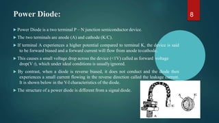
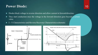
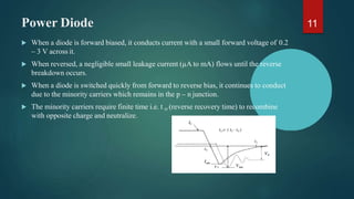
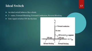
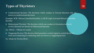
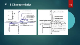
1. Power diodes conduct current in the forward direction and block voltage in the reverse direction. Thyristors can conduct in both directions but require a gate signal to turn on.
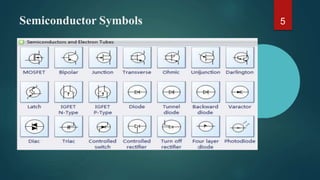
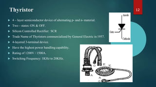
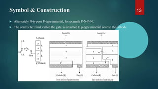
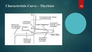
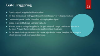
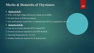
2. Thyristors like SCRs have four alternating layers of p-type and n-type semiconductor material. They can latch on in the conducting state once triggered by a gate signal.
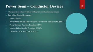
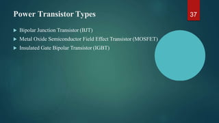
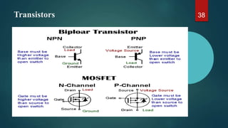
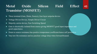
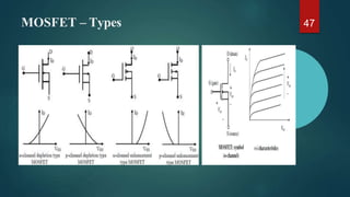
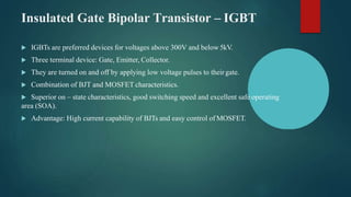
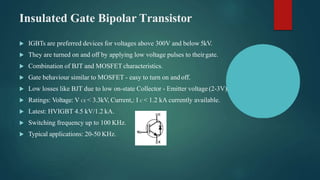
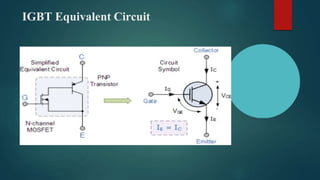
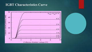
3. Other power semiconductor devices discussed include power MOSFETs, IGBTs, and GTO thyristors. Each