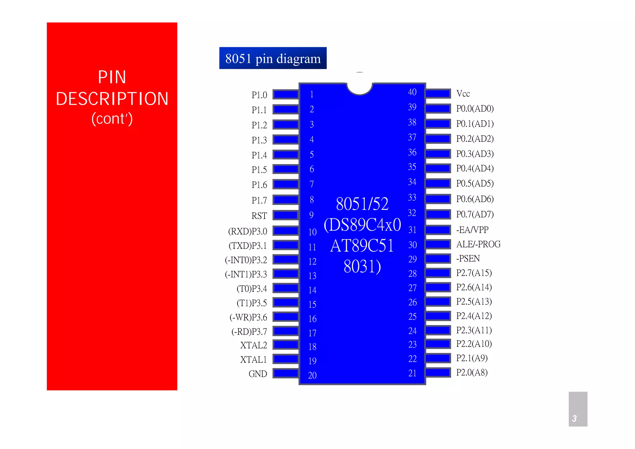
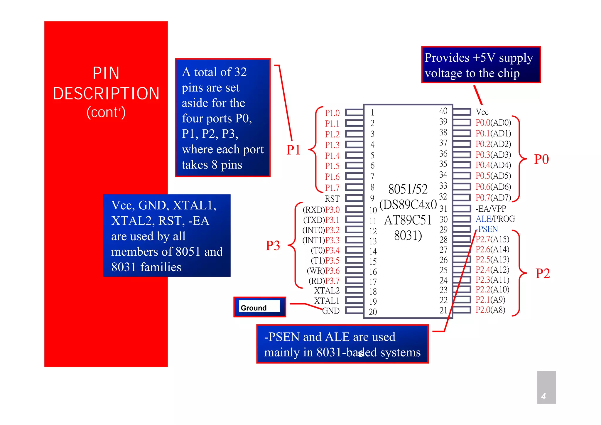
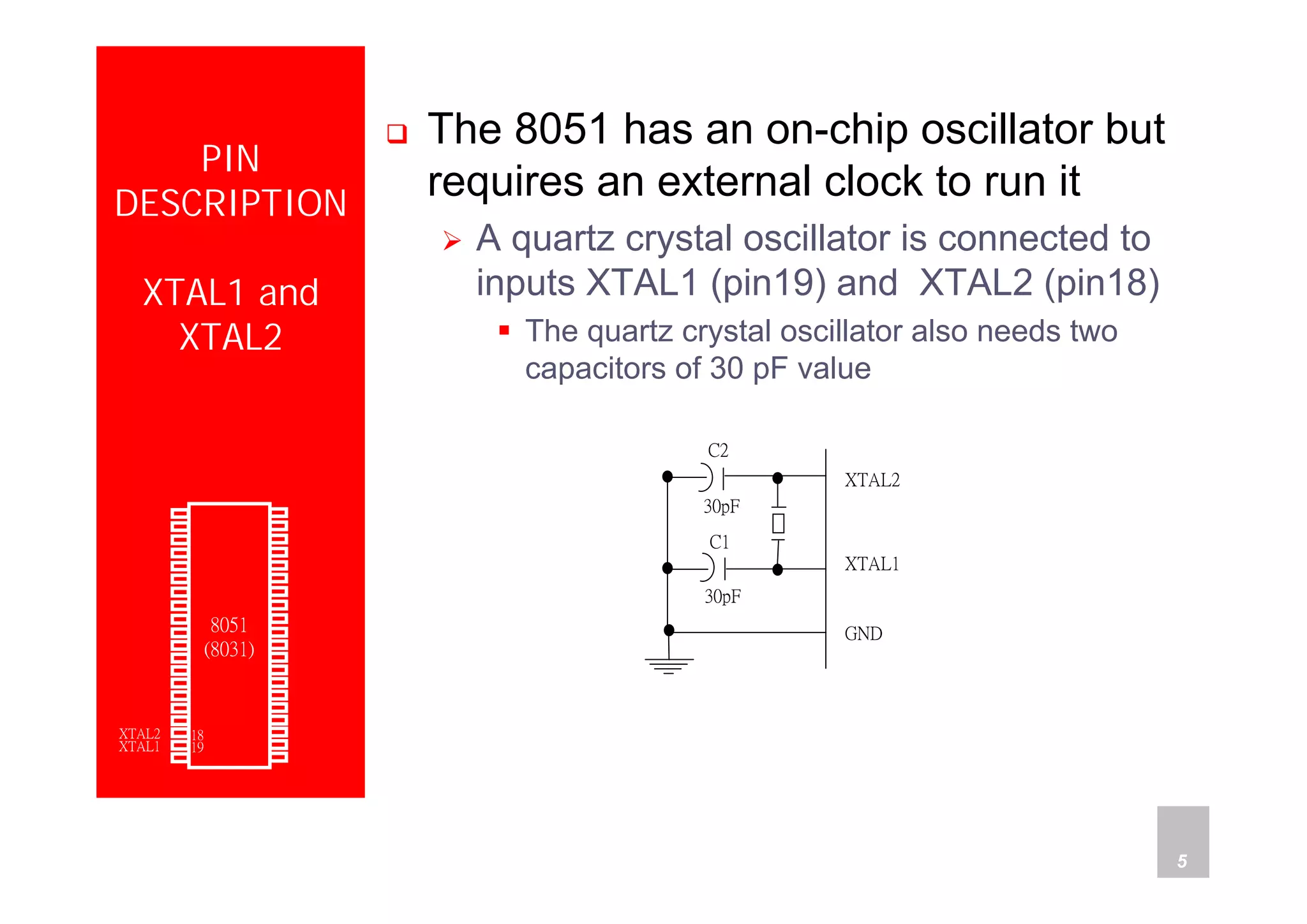
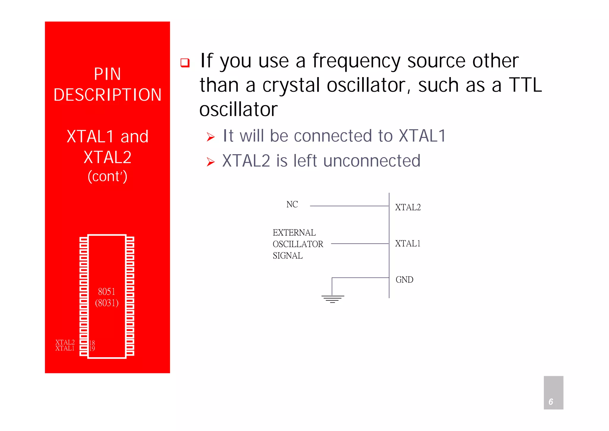
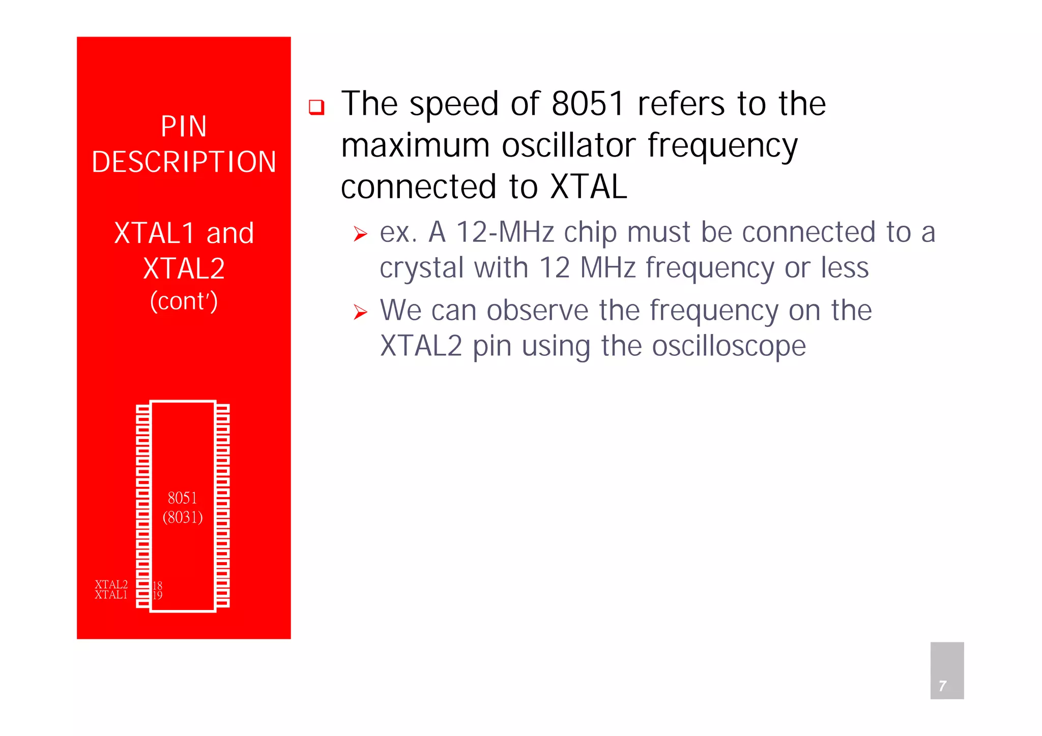
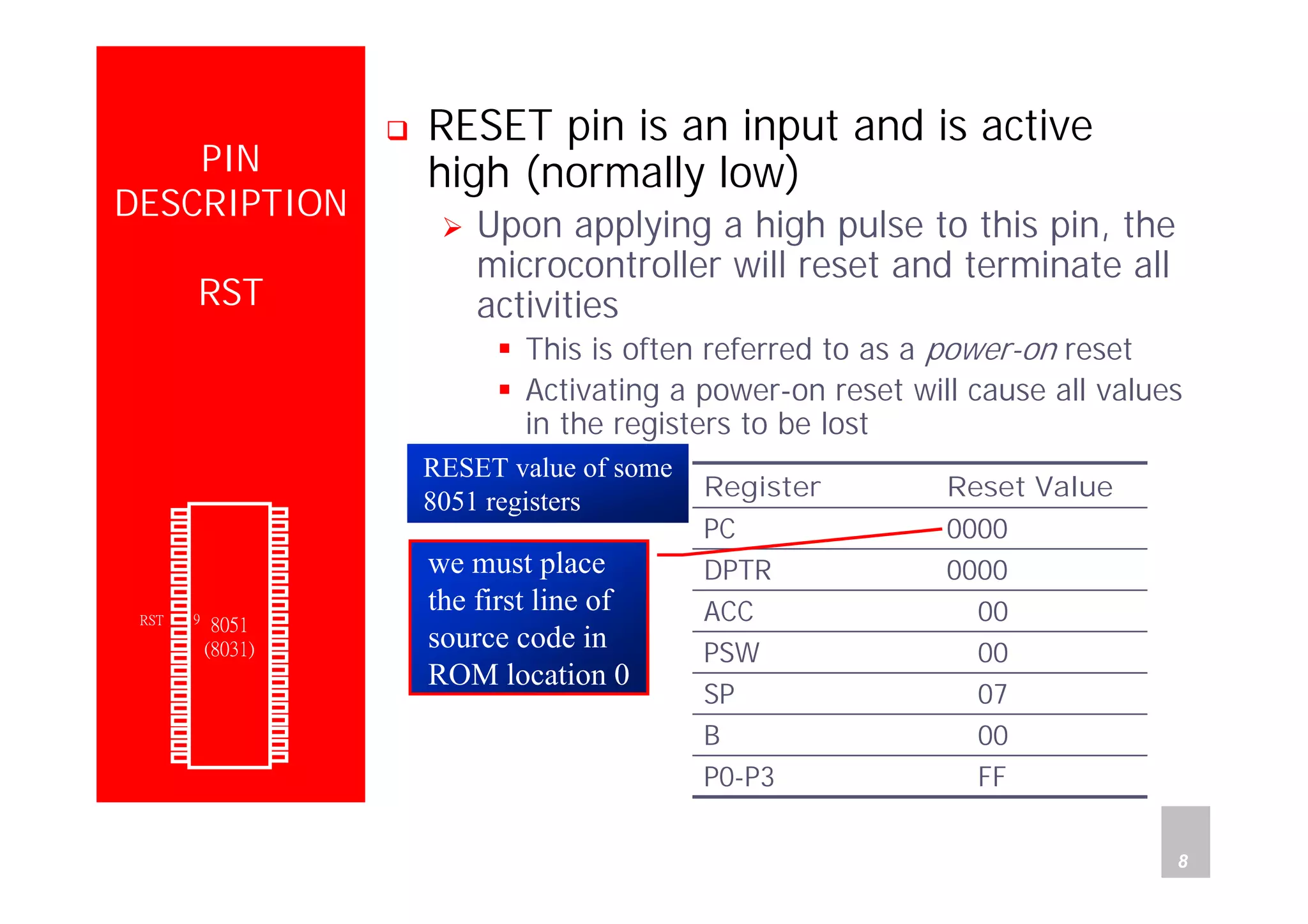
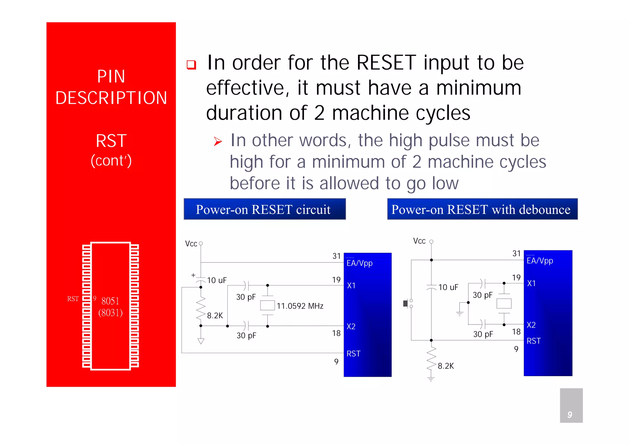
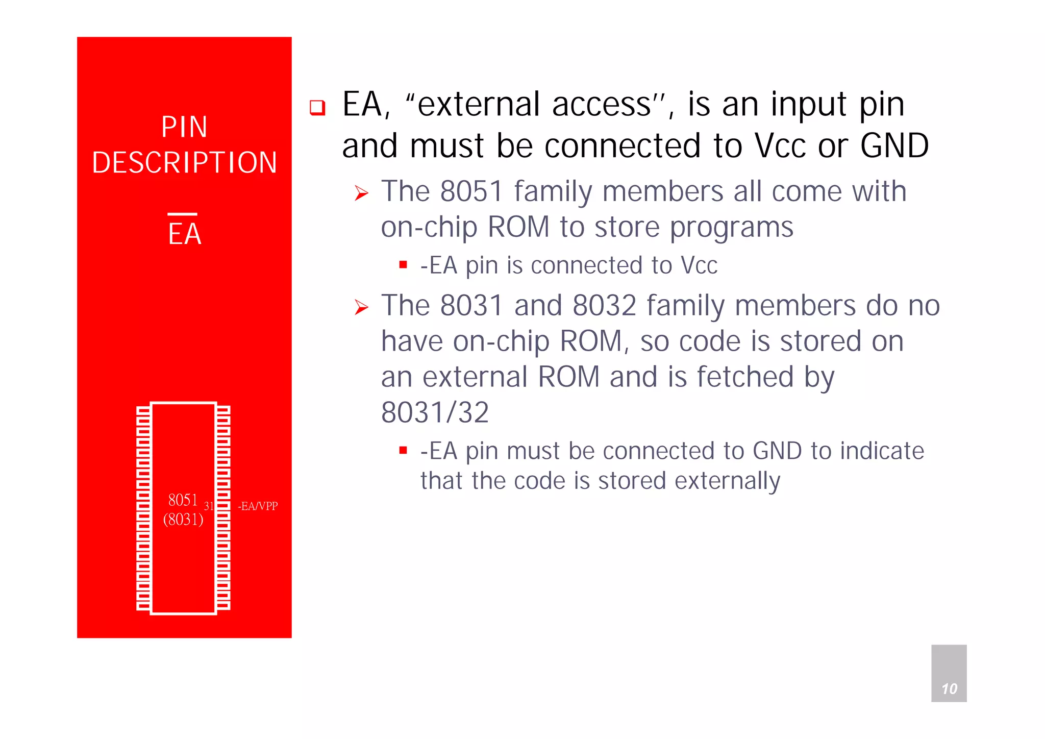
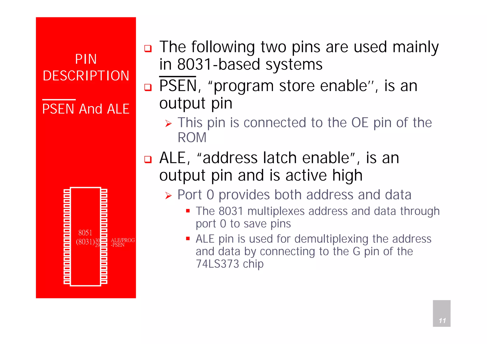
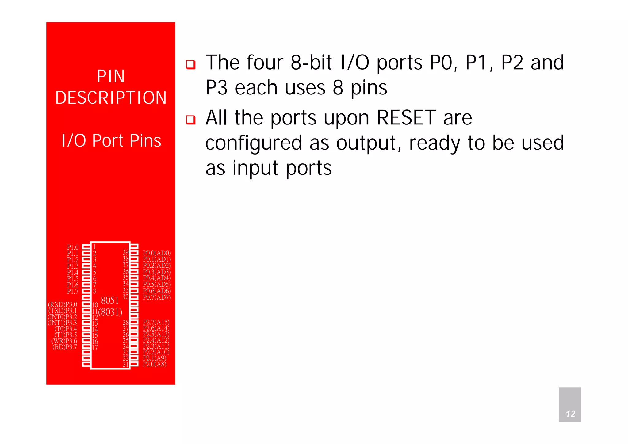
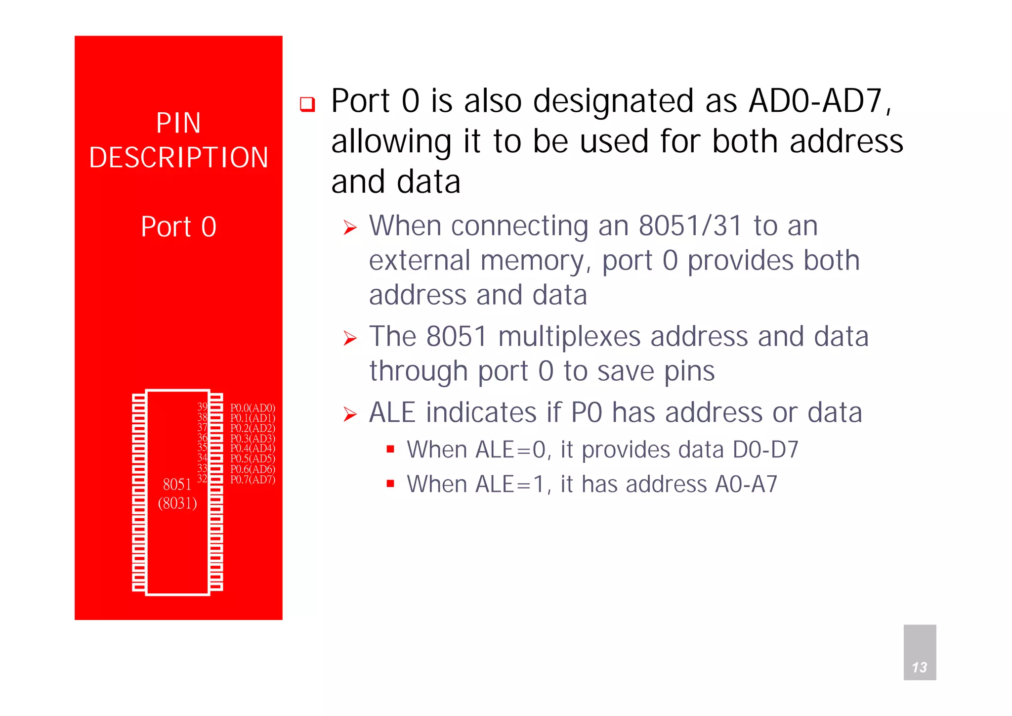
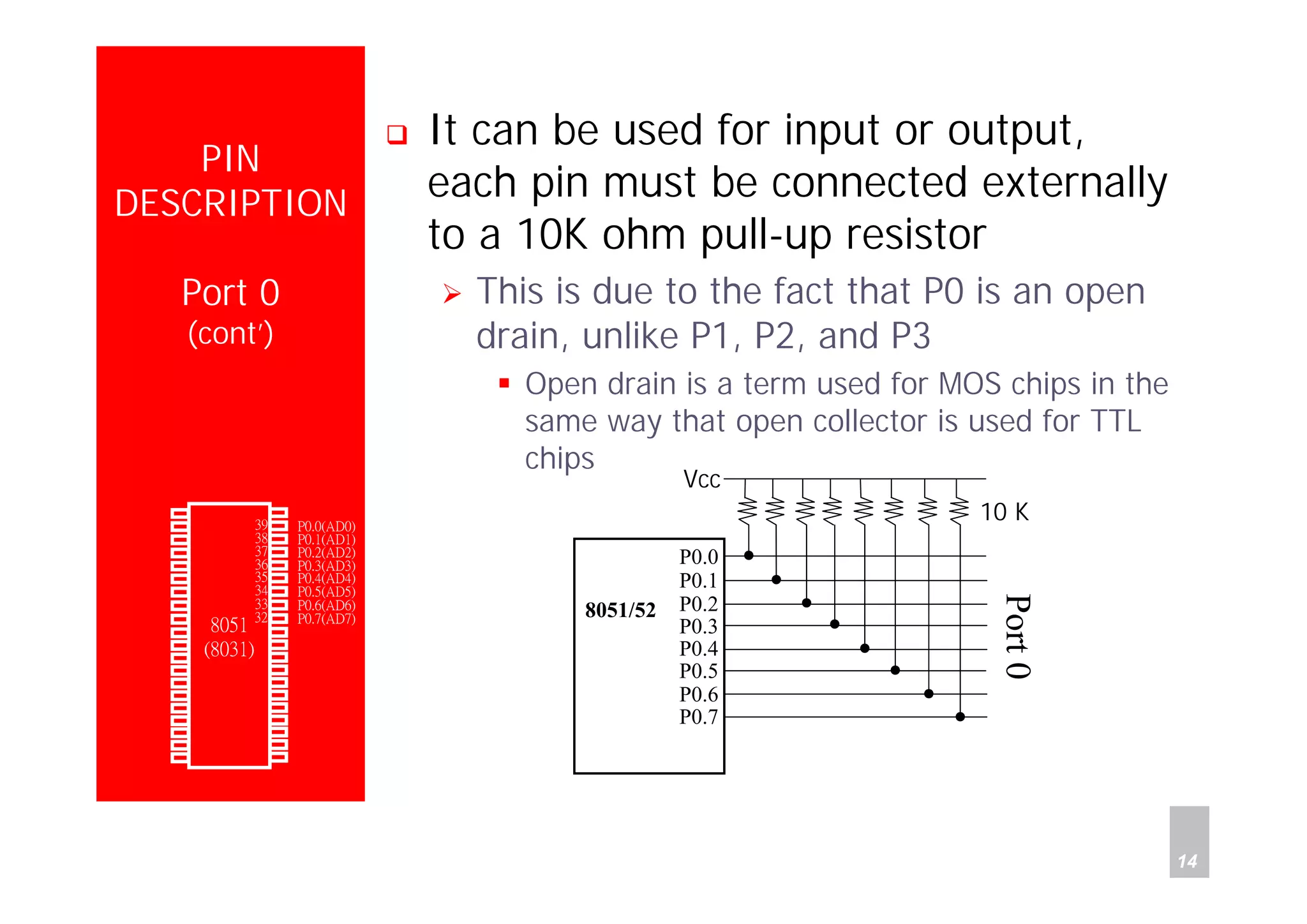
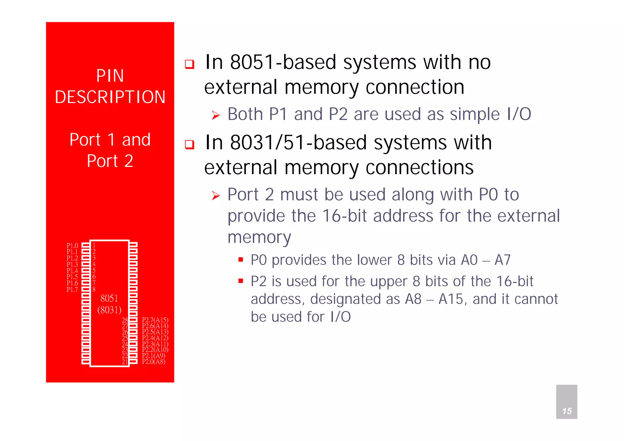
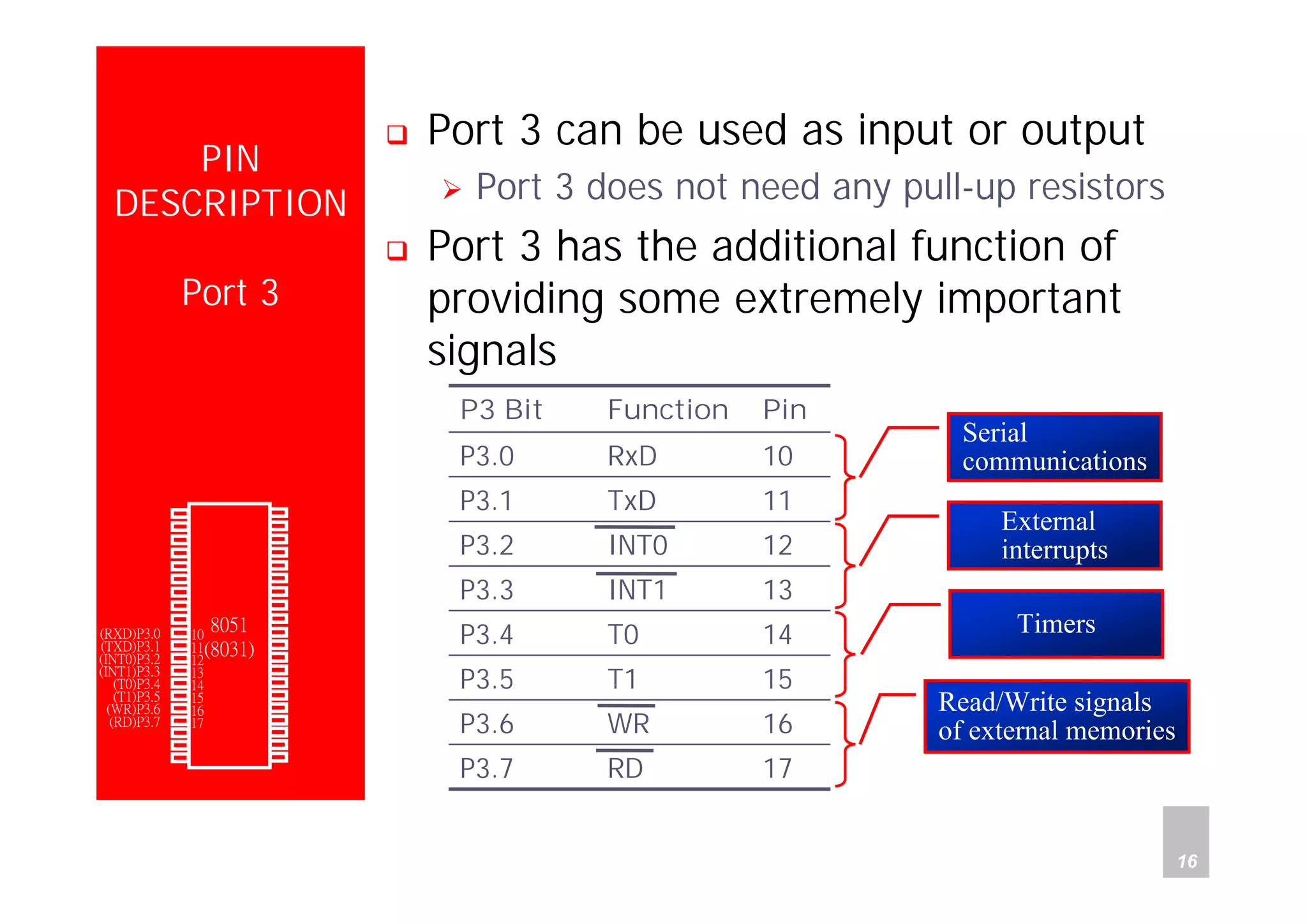
The document describes the pins of the 8051 microcontroller. It discusses the functions of pins such as XTAL1, XTAL2, RST, EA, ports P0-P3, and how they are used to connect the microcontroller to external components like oscillators, memory, and I/O devices. Diagrams are provided to illustrate the pin connections for clock sources, reset circuits, and whether code is stored internally or externally. Key specifications like reset values and required pulse lengths are also mentioned.
This document discusses I/O port programming for the 8051 microcontroller. It describes the four 8-bit I/O ports (P0, P1, P2, P3), how each port has 8 pins and can be configured as an input or output. It provides code examples to continuously output alternating values on Port 0 and make Port 0 and Port 1 function as inputs by writing 1's to their pins. The document also notes that Port 0 has a dual role as address/data pins when connecting an 8051 to external memory.
The document describes the features and specifications of the AT89S51 microcontroller, including its 4K bytes of in-system programmable flash memory, I/O ports, serial communication channel, timers, and interrupt sources. It provides details on the microcontroller's pin configurations for different packages and describes each pin's functions, such as power supply pins, ports for input/output, reset pin, and pins for programming and memory access.
B tech Final Year Projects & Embedded Systems Training Technogroovy India
like our page for more updates:
https://www.facebook.com/Technogroovyindia
With Best Regard's
Technogroovy Systems India Pvt. Ltd.
www.technogroovy.com
Call- +91-9582888121
Whatsapp- +91-8800718323
The P89V51RD2 is an 80C51 microcontroller with 64kB of Flash memory and 1kB of RAM. It has features like In-System Programming, In-Application Programming, and a choice of running at the standard 80C51 clock rate or twice the throughput at the same clock frequency in X2 mode. It includes ports, timers, serial interfaces, and low power modes.
- The document describes infrared remote control receivers from Princeton Technology Corp that utilize CMOS technology.
- The PT2249A series can control 10 functions and is in a 16 pin DIP package. The PT2250A series can control 18 functions and is in a 24 pin DIP package.
- The receivers work with Princeton Technology's PT2248 remote control encoder to receive and decode infrared signals for applications like audio/TV/VCR remote controls.
The AT89C4051 is a low-voltage, high-performance CMOS 8-bit microcontroller with
4K bytes of Flash programmable and erasable read-only memory. The device is manufactured
using Atmel’s high-density nonvolatile memory technology and is
compatible with the industry-standard MCS-51 instruction set. By combining a versatile
8-bit CPU with Flash on a monolithic chip, the Atmel AT89C4051 is a powerful
microcontroller which provides a highly-flexible and cost-effective solution to many
embedded control applications.
The AT89C4051 provides the following standard features: 4K bytes of Flash,
128 bytes of RAM, 15 I/O lines, two 16-bit timer/counters, a five-vector, two-level interrupt
architecture, a full duplex serial port, a precision analog comparator, on-chip
oscillator and clock circuitry. In addition, the AT89C4051 is designed with static logic
for operation down to zero frequency and supports two software-selectable power
saving modes. The Idle Mode stops the CPU while allowing the RAM, timer/counters,
serial port and interrupt system to continue functioning. The power-down mode saves
the RAM contents but freezes the oscillator disabling all other chip functions until the
next hardware reset.
1. A hardware reset which initializes all on-chip registers
including the SFRs.
The AT89C51 is a low-power, high-performance 8-bit micro-
controller with 4K bytes of flash memory. It has 32 I/O lines, 2. Return from a CALL instruction. In this case, the pro-
two 16-bit timer/counters, serial communication capabilities, gram counter (PC) and registers will resume their values
and low-power idle and power-down modes. The document prior to entry into power-down.
provides details on the microcontroller's features, pinout, 3. An external interrupt condition that causes a wake
Logic - Gates and Inverters are available at componentship.com.we offer inventory, pricing, & datasheets for Logic - Gates and Inverters Integrated Circuits (ICs)
http://www.componentschip.com/Integrated-Circuits-(ICs)/Logic-Gates-and-Inverters.html
Logic - Gates and Inverters are available at componentship.com.we offer inventory, pricing, & datasheets for Logic - Gates and Inverters Integrated Circuits (ICs)
http://www.componentschip.com/Integrated-Circuits-(ICs)/Logic-Gates-and-Inverters.html
The document describes the features and specifications of the AT89C2051 microcontroller. It has 2K bytes of flash memory, 128 bytes of RAM, 15 I/O lines, two timers, serial communication capabilities, and low power modes. The microcontroller has various registers and can be programmed to store instructions in flash memory using an algorithm that involves setting control pins and pulsing other pins in a specific sequence.
Electrónica: Receptor DTMF integrado MT8870D/MT8870D-1 (Datasheet)SANTIAGO PABLO ALBERTO
The MT8870D/MT8870D-1 is a complete DTMF receiver integrated circuit that detects DTMF tones. It has a filter section that separates high and low group tones and a digital decoder that detects and decodes the 16 DTMF tone pairs into a 4-bit output code. It has low power consumption and integrates the bandsplit filter and digital decoder functions onto a single chip. The chip can be configured to meet various system requirements by adjusting the external steering time constants to select the guard times for tone detection and interdigital pauses.
This document describes the AT89C51 microcontroller. It has 4K bytes of flash memory, 128 bytes of RAM, 32 I/O lines, two 16-bit timers/counters, a five vector interrupt architecture, a serial port, and on-chip oscillator. It also describes the pin configurations for the microcontroller in PDIP, PLCC, and TQFP packages and provides details on the functions of individual pins.
The document provides a user manual for an 8051 development kit. It includes a 1-2 sentence description of each of the following: the components included in the kit, features of the kit such as its size and included microcontroller, I/O interfaces, and pin connections of the microcontroller. The kit is intended for advanced embedded applications and contains surface mount components on a double sided PCB.
This document summarizes the features of the Atmel ATmega8L and ATmega8 microcontrollers. It includes:
- Details on the 8-bit RISC architecture, registers, speed grades up to 16MHz, and low power consumption.
- On-chip memory features including 8K flash, 512B EEPROM, and 1KB SRAM with high endurance and long data retention.
- Peripheral features such as timers, PWM, ADC, serial interfaces, and analog comparator.
- Package options, pin configurations, and operating voltages from 2.7V to 5.5V.
The document describes the AT89S51 microcontroller. It has 4K bytes of in-system programmable flash memory, 128 bytes of RAM, 32 I/O lines, and features like timers, serial communication, and low power modes. The microcontroller is compatible with the 80C51 instruction set and provides a flexible and cost-effective solution for embedded applications.
The AT89S51 is a low-power, high-performance CMOS 8-bit microcontroller with 4K
bytes of In-System Programmable Flash memory. The device is manufactured using
Atmel’s high-density nonvolatile memory technology and is compatible with the industry-
standard 80C51 instruction set and pinout. The on-chip Flash allows the program
memory to be reprogrammed in-system or by a conventional nonvolatile memory programmer.
By combining a versatile 8-bit CPU with In-System Programmable Flash on
a monolithic chip, the Atmel AT89S51 is a powerful microcontroller which provides a
highly-flexible and cost-effective solution to many embedded control applications.
The AT89S51 provides the following standard features: 4K bytes of Flash, 128 bytes
of RAM, 32 I/O lines, Watchdog timer, two data pointers, two 16-bit timer/counters, a
five-vector two-level interrupt architecture, a full duplex serial port, on-chip oscillator,
and clock circuitry. In addition, the AT89S51 is designed with static logic for operation
down to zero frequency and supports two software selectable power saving modes.
The Idle Mode stops the CPU while allowing the RAM, timer/counters, serial port, and
interrupt system to continue functioning. The Power-down mode saves the RAM contents
but freezes the oscillator, disabling all other chip functions until the next external
interrupt or hardware reset.
8-bit
Microcontroller
with 4K Bytes
In-System
Programmable
Flash
AT89S51
2487D
The document describes the features and specifications of the AT89S52 microcontroller. It includes 8K bytes of in-system programmable flash memory, 256 bytes of RAM, 32 I/O lines, and various timer/counter and serial communication functions. It provides detailed information on the microcontroller's pin configurations, pin descriptions and alternate functions.
This document provides information about a lab manual for a Microcontrollers course. It includes:
1) An index listing 12 experiments covering assembly programming of 8051 microcontrollers and interfacing programs, along with MSP430 programming.
2) Syllabus details for the course outlining topics like data transfer, arithmetic, logic instructions, counters and interfacing modules.
3) Instructions for students on lab protocols and expectations.
4) Table of contents organizing the experiments and programs by topic and page numbers.
5) An introduction section describing 8051 architecture features and Keil μVision tools for programming.
This document provides instructions for programming and setting up an ArgoxScan barcode scanner. It includes information on selecting the interface, keyboard layout, RS-232 settings, enabling supported barcode types, and programming the scanner by scanning setup barcodes. Programming requires scanning barcodes in the provided table in the correct order to configure options like prefix, suffix, symbology settings and more. Pins assignments and connectors are also shown for RS-232, keyboard wedge, and USB connectivity options.
The AT89C52 is a low-power microcontroller with 8K bytes of flash memory. It has 8 I/O lines, 3 timers/counters, a serial port, and supports two power saving modes. The document describes the features of the microcontroller including memory, I/O ports, pins, and special function registers. It provides detailed information on the functions of various pins and registers for timers, interrupts, and other peripherals.
The document contains a flowchart that describes the steps in a sensor monitoring system. It starts with initializing settings and checking the status of the data received. It then reads data from a FIFO buffer, sends the data to a serial port, and checks the interrupt pin status. If data is received, it reads the data and exits. Otherwise it exits. It then initializes the SPI and ADC settings, reads the ADC results from an interface circuit, waits one second, and writes the ADC results to an RF chip before repeating the process.
This document summarizes the features and specifications of the ATmega16 microcontroller. It has a low-power 8-bit AVR processor with 16K bytes of flash memory, 512 bytes of EEPROM, and 1K byte of SRAM. It includes timers, PWM channels, ADC, serial interfaces, and I/O pins. The microcontroller supports in-system programming of its flash memory and operates between 0-16MHz with voltages from 2.7-5.5V.
The document describes an embedded controller evaluation board that contains an AT89C51ED2 microcontroller, LEDs, switches, an LCD display, serial interface, ADC, DAC, RTC, and other peripherals. It provides instructions on applying power, serial communication, and examples of programs to blink LEDs, use timers to delay and toggle an LED, interface with the LCD display, and read a 4x4 keypad. The goal is to help users understand the capabilities of the microcontroller and experiment with its various features.
The AT89S8253 is a low-power 8-bit microcontroller with 12K bytes of flash program memory and 2K bytes of EEPROM data memory. It has various I/O features including ports, timers, serial interface, and interrupts. The flash memory can be reprogrammed in-system through an SPI interface or external programmer, allowing for flexible and cost-effective solutions to embedded applications.
The TX-2B/RX-2B is a pair of CMOS LSIs designed for remote controlled car applications. It has five control keys for controlling motions like forward, backward, right, left, and turbo functions. It features a wide operating voltage range, low stand-by current, and auto-power-off function. Few external components are needed. The TX-2B transmits encoded signals corresponding to the key pressed and the RX-2B receives and decodes the signals to control the car motions.
This document describes the AT89C2051 microcontroller. Key details include:
- It has 2K bytes of reprogrammable flash memory, 128 bytes of RAM, 15 I/O lines, and various timer/counter and communication features.
- Programming the flash memory involves applying the correct signals to ports to write bytes, erase the entire array, or read back data for verification.
- It has low power idle and power down modes for reduced power consumption and various interrupt sources and register addresses.
- The microcontroller is part of Atmel's MCS-51 family and is programmed using the MCS-51 instruction set with some restrictions due to its memory limits.
This document describes the pinout of the 8051 microcontroller. It lists the 40 pins of the 8051 and provides a brief description of the functions of some of the most important pins including ports P0-P3, the reset pin, oscillator pins, VCC, interrupt and counter pins, and pins for interfacing with external memory. The pins allow the 8051 to interface with external devices and memory and function as either inputs or outputs to expand its capabilities.
This document describes the AT89C52 microcontroller. It includes a pinout diagram, brief descriptions of each pin and their alternate functions, a block diagram of the chip architecture, and a table of the Special Function Registers (SFRs) with their reset values. The AT89C52 is an 8-bit microcontroller with 8K bytes of flash memory, 256 bytes of RAM, 32 I/O lines, and other standard features.
This document describes the AT89C51 microcontroller. It includes a pinout diagram and descriptions of the pins including power, ground, ports 0-3, reset, ALE/PROG, PSEN, EA/VPP, oscillator pins, and alternate functions of port 3 pins. It provides a block diagram of the architecture and describes features like 4K bytes of flash memory, 128 bytes of RAM, timers, interrupts, serial port, and power saving idle and power down modes.
The document provides an overview of the 8051 microcontroller, comparing it to microprocessors. It discusses the architecture and features of the 8051, including its on-chip RAM, ROM, I/O ports, and CPU. It also outlines the basic steps for application development using the 8051, such as connecting the power supply and crystal, adding a reset circuit, writing software, and burning the program into ROM.
The 8051 microcontroller is an 8-bit microcontroller commonly used in embedded systems. It has 8KB of ROM, 128 bytes of RAM, four I/O ports, two timers, and supports interrupts. It uses a 12MHz crystal oscillator as its system clock. The CPU fetches and executes instructions from code memory and accesses data memory through an internal address/data bus. It has various special function registers for control and status. Ports are bi-directional and can be configured for input or output through writing/reading values.
The document discusses the 8051 microcontroller. It lists advantages of microcontroller-based systems such as lower cost, smaller size, and higher reliability compared to microprocessor-based systems. It describes some 8051 family members and compares their features such as ROM type, RAM size, and number of timers. It also discusses important components of the 8051 like ROM, RAM, I/O ports, timers, and serial port. The document provides block diagrams of the 8051 internal architecture and pinout. It describes the functions of various pins and registers.
This document provides an overview of the 8051 microcontroller architecture. It describes the basic components of the 8051 including 4K bytes of internal ROM, 128 bytes of internal RAM, four 8-bit I/O ports, two timers/counters, one serial interface, and other features. It also discusses the different addressing modes for 8051 assembly language programming including immediate, register, direct, register indirect, and external direct addressing.
The document provides an overview of the 8051 microcontroller, including its block diagram, pin descriptions, registers, memory mapping, stack, I/O port programming, timers, and interrupts. It explains the basic components and architecture of the 8051, how it maps memory and handles interrupts and timers. It also compares microprocessors to microcontrollers and discusses embedded systems.
Presentation On: "Micro-controller 8051 & Embedded System"surabhii007
The presentation is dealing with majors about 'An Embedded System' along with 'Micro-controller' with it's base peripherals & parameters.
Hope It'll be helpfull!
An embedded system is closely integrated with the main system
It may not interact directly with the environment
For example – A microcomputer in a car ignition control
This document provides an overview of the 8051 microcontroller, including its basic components, registers, memory mapping, stack, I/O port programming, timers, and interrupts. It begins with an introduction and block diagram of the 8051 and descriptions of its pins and registers. It then discusses the 8051's memory mapping and stack, as well as how to program its I/O ports, timers, and interrupts. The document also compares microprocessors and microcontrollers, describing the 8051 as a single-chip microcontroller with on-chip RAM, ROM, I/O ports, and other components. It provides examples of the 8051's use in embedded systems for applications requiring low cost, power, and space.
8051 microcontroller training (sahil gupta 9068557926)Sahil Gupta
The document provides information on microprocessors and microcontrollers. It discusses that microprocessors are the core of computer systems and are now used to control many communication, entertainment and portable devices. Microprocessors have separate RAM, ROM, I/O components whereas microcontrollers have these components integrated on a single chip. The document then discusses the basic components of a microprocessor system including the CPU, memory types, buses, timers and ports. It provides examples of common microprocessors and microcontrollers and their applications. Key selection criteria for choosing a microcontroller include meeting computing needs efficiently, availability of development tools and source reliability.
The document describes the AT89C51 microcontroller, including its features, pin descriptions, block diagram, and programming details. Key points:
- It has 4K bytes of flash memory, 128 bytes of RAM, 32 I/O lines, two timers, serial port, and low power modes.
- Pins described include ports 0-3, reset, clock, and power pins. Ports have pullups and alternate functions like serial I/O.
- Block diagram shows CPU, memory, I/O, and peripheral blocks.
- Programming interface supports low or high voltage modes for in-system or external programming of flash memory.
This document discusses an embedded systems presentation submitted by Amandeep Singh. It provides definitions and examples of embedded systems, noting they are designed for specific applications like industrial machines, medical equipment, and toys. It also summarizes key aspects of embedded system components like microcontrollers, addressing modes, and applications. Recent examples highlighted are devices that aid communication for the deaf, integrate weighing and dimension measuring, and allow adjustable cushioning in smart shoes.
The document discusses the Microcontroller 8051. It provides a block diagram and pin description of the 8051. It describes the registers, memory mapping, stack, I/O ports, timers and interrupts of the 8051 microcontroller. It compares microprocessors and microcontrollers, discussing the differences in hardware structure and applications.
The AT89C51 is a low-power, high-performance 8-bit microcontroller with 4K bytes of flash memory. It has 32 I/O lines, two 16-bit timer counters, serial communication capabilities, and on-chip programming. The device operates between 0 and 24 MHz and has various power saving modes like idle and power down to reduce power consumption. It is compatible with the MCS-51 instruction set and provides a cost-effective solution for embedded applications.
Ei502microprocessorsmicrtocontrollerspart4 8051 MicrocontrollerDebasis Das
The document discusses the applications and features of microcontrollers. It provides examples of using microcontrollers for interfacing seven segment displays, temperature control, and other applications. It also discusses where microcontrollers can commonly be found, such as in cell phones, laptops, appliances, toys and more. The document outlines reasons for learning about microprocessors/controllers and provides an overview of the 8051 microcontroller, including its architecture, pins, registers and memory mapping.
The 8051 microcontroller is a Harvard architecture microcontroller developed by Intel in 1980 for use in embedded systems. It has separate program and data memories, 4 I/O ports, two 16-bit timers, a serial port, and can address up to 64KB of external memory. The 8051 has become widely used due to its low cost and availability of development tools from multiple manufacturers. It has a simple but powerful instruction set that can be easily learned, making it well suited for embedded applications.
A review on techniques and modelling methodologies used for checking electrom...nooriasukmaningtyas
The proper function of the integrated circuit (IC) in an inhibiting electromagnetic environment has always been a serious concern throughout the decades of revolution in the world of electronics, from disjunct devices to today’s integrated circuit technology, where billions of transistors are combined on a single chip. The automotive industry and smart vehicles in particular, are confronting design issues such as being prone to electromagnetic interference (EMI). Electronic control devices calculate incorrect outputs because of EMI and sensors give misleading values which can prove fatal in case of automotives. In this paper, the authors have non exhaustively tried to review research work concerned with the investigation of EMI in ICs and prediction of this EMI using various modelling methodologies and measurement setups.
Using recycled concrete aggregates (RCA) for pavements is crucial to achieving sustainability. Implementing RCA for new pavement can minimize carbon footprint, conserve natural resources, reduce harmful emissions, and lower life cycle costs. Compared to natural aggregate (NA), RCA pavement has fewer comprehensive studies and sustainability assessments.
A SYSTEMATIC RISK ASSESSMENT APPROACH FOR SECURING THE SMART IRRIGATION SYSTEMSIJNSA Journal
The smart irrigation system represents an innovative approach to optimize water usage in agricultural and landscaping practices. The integration of cutting-edge technologies, including sensors, actuators, and data analysis, empowers this system to provide accurate monitoring and control of irrigation processes by leveraging real-time environmental conditions. The main objective of a smart irrigation system is to optimize water efficiency, minimize expenses, and foster the adoption of sustainable water management methods. This paper conducts a systematic risk assessment by exploring the key components/assets and their functionalities in the smart irrigation system. The crucial role of sensors in gathering data on soil moisture, weather patterns, and plant well-being is emphasized in this system. These sensors enable intelligent decision-making in irrigation scheduling and water distribution, leading to enhanced water efficiency and sustainable water management practices. Actuators enable automated control of irrigation devices, ensuring precise and targeted water delivery to plants. Additionally, the paper addresses the potential threat and vulnerabilities associated with smart irrigation systems. It discusses limitations of the system, such as power constraints and computational capabilities, and calculates the potential security risks. The paper suggests possible risk treatment methods for effective secure system operation. In conclusion, the paper emphasizes the significant benefits of implementing smart irrigation systems, including improved water conservation, increased crop yield, and reduced environmental impact. Additionally, based on the security analysis conducted, the paper recommends the implementation of countermeasures and security approaches to address vulnerabilities and ensure the integrity and reliability of the system. By incorporating these measures, smart irrigation technology can revolutionize water management practices in agriculture, promoting sustainability, resource efficiency, and safeguarding against potential security threats.
TIME DIVISION MULTIPLEXING TECHNIQUE FOR COMMUNICATION SYSTEMHODECEDSIET
Time Division Multiplexing (TDM) is a method of transmitting multiple signals over a single communication channel by dividing the signal into many segments, each having a very short duration of time. These time slots are then allocated to different data streams, allowing multiple signals to share the same transmission medium efficiently. TDM is widely used in telecommunications and data communication systems.
### How TDM Works
1. **Time Slots Allocation**: The core principle of TDM is to assign distinct time slots to each signal. During each time slot, the respective signal is transmitted, and then the process repeats cyclically. For example, if there are four signals to be transmitted, the TDM cycle will divide time into four slots, each assigned to one signal.
2. **Synchronization**: Synchronization is crucial in TDM systems to ensure that the signals are correctly aligned with their respective time slots. Both the transmitter and receiver must be synchronized to avoid any overlap or loss of data. This synchronization is typically maintained by a clock signal that ensures time slots are accurately aligned.
3. **Frame Structure**: TDM data is organized into frames, where each frame consists of a set of time slots. Each frame is repeated at regular intervals, ensuring continuous transmission of data streams. The frame structure helps in managing the data streams and maintaining the synchronization between the transmitter and receiver.
4. **Multiplexer and Demultiplexer**: At the transmitting end, a multiplexer combines multiple input signals into a single composite signal by assigning each signal to a specific time slot. At the receiving end, a demultiplexer separates the composite signal back into individual signals based on their respective time slots.
### Types of TDM
1. **Synchronous TDM**: In synchronous TDM, time slots are pre-assigned to each signal, regardless of whether the signal has data to transmit or not. This can lead to inefficiencies if some time slots remain empty due to the absence of data.
2. **Asynchronous TDM (or Statistical TDM)**: Asynchronous TDM addresses the inefficiencies of synchronous TDM by allocating time slots dynamically based on the presence of data. Time slots are assigned only when there is data to transmit, which optimizes the use of the communication channel.
### Applications of TDM
- **Telecommunications**: TDM is extensively used in telecommunication systems, such as in T1 and E1 lines, where multiple telephone calls are transmitted over a single line by assigning each call to a specific time slot.
- **Digital Audio and Video Broadcasting**: TDM is used in broadcasting systems to transmit multiple audio or video streams over a single channel, ensuring efficient use of bandwidth.
- **Computer Networks**: TDM is used in network protocols and systems to manage the transmission of data from multiple sources over a single network medium.
### Advantages of TDM
- **Efficient Use of Bandwidth**: TDM all
Comparative analysis between traditional aquaponics and reconstructed aquapon...bijceesjournal
The aquaponic system of planting is a method that does not require soil usage. It is a method that only needs water, fish, lava rocks (a substitute for soil), and plants. Aquaponic systems are sustainable and environmentally friendly. Its use not only helps to plant in small spaces but also helps reduce artificial chemical use and minimizes excess water use, as aquaponics consumes 90% less water than soil-based gardening. The study applied a descriptive and experimental design to assess and compare conventional and reconstructed aquaponic methods for reproducing tomatoes. The researchers created an observation checklist to determine the significant factors of the study. The study aims to determine the significant difference between traditional aquaponics and reconstructed aquaponics systems propagating tomatoes in terms of height, weight, girth, and number of fruits. The reconstructed aquaponics system’s higher growth yield results in a much more nourished crop than the traditional aquaponics system. It is superior in its number of fruits, height, weight, and girth measurement. Moreover, the reconstructed aquaponics system is proven to eliminate all the hindrances present in the traditional aquaponics system, which are overcrowding of fish, algae growth, pest problems, contaminated water, and dead fish.
DEEP LEARNING FOR SMART GRID INTRUSION DETECTION: A HYBRID CNN-LSTM-BASED MODELgerogepatton
As digital technology becomes more deeply embedded in power systems, protecting the communication
networks of Smart Grids (SG) has emerged as a critical concern. Distributed Network Protocol 3 (DNP3)
represents a multi-tiered application layer protocol extensively utilized in Supervisory Control and Data
Acquisition (SCADA)-based smart grids to facilitate real-time data gathering and control functionalities.
Robust Intrusion Detection Systems (IDS) are necessary for early threat detection and mitigation because
of the interconnection of these networks, which makes them vulnerable to a variety of cyberattacks. To
solve this issue, this paper develops a hybrid Deep Learning (DL) model specifically designed for intrusion
detection in smart grids. The proposed approach is a combination of the Convolutional Neural Network
(CNN) and the Long-Short-Term Memory algorithms (LSTM). We employed a recent intrusion detection
dataset (DNP3), which focuses on unauthorized commands and Denial of Service (DoS) cyberattacks, to
train and test our model. The results of our experiments show that our CNN-LSTM method is much better
at finding smart grid intrusions than other deep learning algorithms used for classification. In addition,
our proposed approach improves accuracy, precision, recall, and F1 score, achieving a high detection
accuracy rate of 99.50%.
Presentation of IEEE Slovenia CIS (Computational Intelligence Society) Chapte...University of Maribor
Slides from talk presenting:
Aleš Zamuda: Presentation of IEEE Slovenia CIS (Computational Intelligence Society) Chapter and Networking.
Presentation at IcETRAN 2024 session:
"Inter-Society Networking Panel GRSS/MTT-S/CIS
Panel Session: Promoting Connection and Cooperation"
IEEE Slovenia GRSS
IEEE Serbia and Montenegro MTT-S
IEEE Slovenia CIS
11TH INTERNATIONAL CONFERENCE ON ELECTRICAL, ELECTRONIC AND COMPUTING ENGINEERING
3-6 June 2024, Niš, Serbia
ACEP Magazine edition 4th launched on 05.06.2024Rahul
This document provides information about the third edition of the magazine "Sthapatya" published by the Association of Civil Engineers (Practicing) Aurangabad. It includes messages from current and past presidents of ACEP, memories and photos from past ACEP events, information on life time achievement awards given by ACEP, and a technical article on concrete maintenance, repairs and strengthening. The document highlights activities of ACEP and provides a technical educational article for members.
1. Home Automation, Networking, and Entertainment Lab
Dept. of Computer Science and Information Engineering
National Cheng Kung University, TAIWAN
Chung-Ping Young
楊中平
HARDWARE CONNECTION
AND INTEL HEX FILE
The 8051 Microcontroller and Embedded
Systems: Using Assembly and C
Mazidi, Mazidi and McKinlay
HARDWARE CONNECTION
AND
INTEL HEX FILE
2. Department of Computer Science and Information Engineering
National Cheng Kung University, TAIWAN 2
HANEL
PIN
DESCRIPTION
8051 family members (e.g, 8751,
89C51, 89C52, DS89C4x0)
Have 40 pins dedicated for various
functions such as I/O, -RD, -WR, address,
data, and interrupts
Come in different packages, such as
DIP(dual in-line package),
QFP(quad flat package), and
LLC(leadless chip carrier)
Some companies provide a 20-pin version
of the 8051 with a reduced number of
I/O ports for less demanding applications
4. Department of Computer Science and Information Engineering
National Cheng Kung University, TAIWAN 4
HANEL
PIN
DESCRIPTION
(cont’)
8051/52
(DS89C4x0
AT89C51
8031)
P1.0
P1.1
P1.2
P1.3
P1.4
P1.5
P1.6
P1.7
RST
(RXD)P3.0
(TXD)P3.1
(INT0)P3.2
(INT1)P3.3
(T0)P3.4
(T1)P3.5
(WR)P3.6
(RD)P3.7
XTAL2
XTAL1
GND
Vcc
P0.0(AD0)
P0.1(AD1)
P0.2(AD2)
P0.3(AD3)
P0.4(AD4)
P0.5(AD5)
P0.6(AD6)
P0.7(AD7)
-EA/VPP
ALE/PROG
-PSEN
P2.7(A15)
P2.6(A14)
P2.5(A13)
P2.4(A12)
P2.3(A11)
P2.2(A10)
P2.1(A9)
P2.0(A8)
1
2
3
4
5
6
7
8
9
10
11
12
13
14
15
16
17
18
19
20
40
39
38
37
36
35
34
33
32
31
30
29
28
27
26
25
24
23
22
21
A total of 32
pins are set
aside for the
four ports P0,
P1, P2, P3,
where each port
takes 8 pins
Grond
-PSEN and ALE are used
mainly in 8031-baded systems
Vcc, GND, XTAL1,
XTAL2, RST, -EA
are used by all
members of 8051 and
8031 families
P1
P3
P2
P0
Provides +5V supply
voltage to the chip
Ground
s
5. Department of Computer Science and Information Engineering
National Cheng Kung University, TAIWAN 5
HANEL
PIN
DESCRIPTION
XTAL1 and
XTAL2
The 8051 has an on-chip oscillator but
requires an external clock to run it
A quartz crystal oscillator is connected to
inputs XTAL1 (pin19) and XTAL2 (pin18)
The quartz crystal oscillator also needs two
capacitors of 30 pF value
XTAL2
XTAL1
GND
C2
C1
30pF
30pF
P1.0
P1.1
P1.2
P1.3
P1.4
P1.5
P1.6
P1.7
RST
(RXD)P3.0
(TXD)P3.1
(INT0)P3.2
(INT1)P3.3
(T0)P3.4
(T1)P3.5
(WR)P3.6
(RD)P3.7
XTAL2
XTAL1
GND
8051
(8031)
Vcc
P0.0(AD0)
P0.1(AD1)
P0.2(AD2)
P0.3(AD3)
P0.4(AD4)
P0.5(AD5)
P0.6(AD6)
P0.7(AD7)
-EA/VPP
ALE/PROG
-PSEN
P2.7(A15)
P2.6(A14)
P2.5(A13)
P2.4(A12)
P2.3(A11)
P2.2(A10)
P2.1(A9)
P2.0(A8)
1
2
3
4
5
6
7
8
9
10
11
12
13
14
15
16
17
18
19
20
40
39
38
37
36
35
34
33
32
31
30
29
28
27
26
25
24
23
22
21
6. Department of Computer Science and Information Engineering
National Cheng Kung University, TAIWAN 6
HANEL
PIN
DESCRIPTION
XTAL1 and
XTAL2
(cont’)
If you use a frequency source other
than a crystal oscillator, such as a TTL
oscillator
It will be connected to XTAL1
XTAL2 is left unconnected
XTAL2
XTAL1
GND
NC
EXTERNAL
OSCILLATOR
SIGNAL
P1.0
P1.1
P1.2
P1.3
P1.4
P1.5
P1.6
P1.7
RST
(RXD)P3.0
(TXD)P3.1
(INT0)P3.2
(INT1)P3.3
(T0)P3.4
(T1)P3.5
(WR)P3.6
(RD)P3.7
XTAL2
XTAL1
GND
Vcc
P0.0(AD0)
P0.1(AD1)
P0.2(AD2)
P0.3(AD3)
P0.4(AD4)
P0.5(AD5)
P0.6(AD6)
P0.7(AD7)
-EA/VPP
ALE/PROG
-PSEN
P2.7(A15)
P2.6(A14)
P2.5(A13)
P2.4(A12)
P2.3(A11)
P2.2(A10)
P2.1(A9)
P2.0(A8)
1
2
3
4
5
6
7
8
9
10
11
12
13
14
15
16
17
18
19
20
40
39
38
37
36
35
34
33
32
31
30
29
28
27
26
25
24
23
22
21
8051
(8031)
7. Department of Computer Science and Information Engineering
National Cheng Kung University, TAIWAN 7
HANEL
PIN
DESCRIPTION
XTAL1 and
XTAL2
(cont’)
The speed of 8051 refers to the
maximum oscillator frequency
connected to XTAL
ex. A 12-MHz chip must be connected to a
crystal with 12 MHz frequency or less
We can observe the frequency on the
XTAL2 pin using the oscilloscope
P1.0
P1.1
P1.2
P1.3
P1.4
P1.5
P1.6
P1.7
RST
(RXD)P3.0
(TXD)P3.1
(INT0)P3.2
(INT1)P3.3
(T0)P3.4
(T1)P3.5
(WR)P3.6
(RD)P3.7
XTAL2
XTAL1
GND
Vcc
P0.0(AD0)
P0.1(AD1)
P0.2(AD2)
P0.3(AD3)
P0.4(AD4)
P0.5(AD5)
P0.6(AD6)
P0.7(AD7)
-EA/VPP
ALE/PROG
-PSEN
P2.7(A15)
P2.6(A14)
P2.5(A13)
P2.4(A12)
P2.3(A11)
P2.2(A10)
P2.1(A9)
P2.0(A8)
1
2
3
4
5
6
7
8
9
10
11
12
13
14
15
16
17
18
19
20
40
39
38
37
36
35
34
33
32
31
30
29
28
27
26
25
24
23
22
21
8051
(8031)
8. Department of Computer Science and Information Engineering
National Cheng Kung University, TAIWAN 8
HANEL
PIN
DESCRIPTION
RST
RESET pin is an input and is active
high (normally low)
Upon applying a high pulse to this pin, the
microcontroller will reset and terminate all
activities
This is often referred to as a power-on reset
Activating a power-on reset will cause all values
in the registers to be lost
00B
P0-P3
SP
PSW
ACC
DPTR
PC
Register
FF
07
00
00
0000
0000
Reset Value
RESET value of some
8051 registers
we must place
the first line of
source code in
ROM location 0
P1.0
P1.1
P1.2
P1.3
P1.4
P1.5
P1.6
P1.7
RST
(RXD)P3.0
(TXD)P3.1
(INT0)P3.2
(INT1)P3.3
(T0)P3.4
(T1)P3.5
(WR)P3.6
(RD)P3.7
XTAL2
XTAL1
GND
Vcc
P0.0(AD0)
P0.1(AD1)
P0.2(AD2)
P0.3(AD3)
P0.4(AD4)
P0.5(AD5)
P0.6(AD6)
P0.7(AD7)
-EA/VPP
ALE/PROG
-PSEN
P2.7(A15)
P2.6(A14)
P2.5(A13)
P2.4(A12)
P2.3(A11)
P2.2(A10)
P2.1(A9)
P2.0(A8)
1
2
3
4
5
6
7
8
9
10
11
12
13
14
15
16
17
18
19
20
40
39
38
37
36
35
34
33
32
31
30
29
28
27
26
25
24
23
22
21
8051
(8031)
9. Department of Computer Science and Information Engineering
National Cheng Kung University, TAIWAN 9
HANEL
PIN
DESCRIPTION
RST
(cont’)
In order for the RESET input to be
effective, it must have a minimum
duration of 2 machine cycles
In other words, the high pulse must be
high for a minimum of 2 machine cycles
before it is allowed to go low
Power-on RESET circuit Power-on RESET with debounce
8.2K
Vcc
30 pF
30 pF
11.0592 MHz
+
31
19
18
9
EA/Vpp
X1
X2
RST
10 uF
8.2K
Vcc
30 pF
30 pF
31
19
18
9
EA/Vpp
X1
X2
RST
10 uF
P1.0
P1.1
P1.2
P1.3
P1.4
P1.5
P1.6
P1.7
RST
(RXD)P3.0
(TXD)P3.1
(INT0)P3.2
(INT1)P3.3
(T0)P3.4
(T1)P3.5
(WR)P3.6
(RD)P3.7
XTAL2
XTAL1
GND
Vcc
P0.0(AD0)
P0.1(AD1)
P0.2(AD2)
P0.3(AD3)
P0.4(AD4)
P0.5(AD5)
P0.6(AD6)
P0.7(AD7)
-EA/VPP
ALE/PROG
-PSEN
P2.7(A15)
P2.6(A14)
P2.5(A13)
P2.4(A12)
P2.3(A11)
P2.2(A10)
P2.1(A9)
P2.0(A8)
1
2
3
4
5
6
7
8
9
10
11
12
13
14
15
16
17
18
19
20
40
39
38
37
36
35
34
33
32
31
30
29
28
27
26
25
24
23
22
21
8051
(8031)
10. Department of Computer Science and Information Engineering
National Cheng Kung University, TAIWAN 10
HANEL
PIN
DESCRIPTION
EA
EA, “external access’’, is an input pin
and must be connected to Vcc or GND
The 8051 family members all come with
on-chip ROM to store programs
-EA pin is connected to Vcc
The 8031 and 8032 family members do no
have on-chip ROM, so code is stored on
an external ROM and is fetched by
8031/32
-EA pin must be connected to GND to indicate
that the code is stored externally
P1.0
P1.1
P1.2
P1.3
P1.4
P1.5
P1.6
P1.7
RST
(RXD)P3.0
(TXD)P3.1
(INT0)P3.2
(INT1)P3.3
(T0)P3.4
(T1)P3.5
(WR)P3.6
(RD)P3.7
XTAL2
XTAL1
GND
Vcc
P0.0(AD0)
P0.1(AD1)
P0.2(AD2)
P0.3(AD3)
P0.4(AD4)
P0.5(AD5)
P0.6(AD6)
P0.7(AD7)
-EA/VPP
ALE/PROG
-PSEN
P2.7(A15)
P2.6(A14)
P2.5(A13)
P2.4(A12)
P2.3(A11)
P2.2(A10)
P2.1(A9)
P2.0(A8)
1
2
3
4
5
6
7
8
9
10
11
12
13
14
15
16
17
18
19
20
40
39
38
37
36
35
34
33
32
31
30
29
28
27
26
25
24
23
22
21
8051
(8031)
11. Department of Computer Science and Information Engineering
National Cheng Kung University, TAIWAN 11
HANEL
PIN
DESCRIPTION
PSEN And ALE
The following two pins are used mainly
in 8031-based systems
PSEN, “program store enable’’, is an
output pin
This pin is connected to the OE pin of the
ROM
ALE, “address latch enable”, is an
output pin and is active high
Port 0 provides both address and data
The 8031 multiplexes address and data through
port 0 to save pins
ALE pin is used for demultiplexing the address
and data by connecting to the G pin of the
74LS373 chip
P1.0
P1.1
P1.2
P1.3
P1.4
P1.5
P1.6
P1.7
RST
(RXD)P3.0
(TXD)P3.1
(INT0)P3.2
(INT1)P3.3
(T0)P3.4
(T1)P3.5
(WR)P3.6
(RD)P3.7
XTAL2
XTAL1
GND
Vcc
P0.0(AD0)
P0.1(AD1)
P0.2(AD2)
P0.3(AD3)
P0.4(AD4)
P0.5(AD5)
P0.6(AD6)
P0.7(AD7)
-EA/VPP
ALE/PROG
-PSEN
P2.7(A15)
P2.6(A14)
P2.5(A13)
P2.4(A12)
P2.3(A11)
P2.2(A10)
P2.1(A9)
P2.0(A8)
1
2
3
4
5
6
7
8
9
10
11
12
13
14
15
16
17
18
19
20
40
39
38
37
36
35
34
33
32
31
30
29
28
27
26
25
24
23
22
21
8051
(8031)
12. Department of Computer Science and Information Engineering
National Cheng Kung University, TAIWAN 12
HANEL
PIN
DESCRIPTION
I/O Port Pins
The four 8-bit I/O ports P0, P1, P2 and
P3 each uses 8 pins
All the ports upon RESET are
configured as output, ready to be used
as input ports
P1.0
P1.1
P1.2
P1.3
P1.4
P1.5
P1.6
P1.7
RST
(RXD)P3.0
(TXD)P3.1
(INT0)P3.2
(INT1)P3.3
(T0)P3.4
(T1)P3.5
(WR)P3.6
(RD)P3.7
XTAL2
XTAL1
GND
Vcc
P0.0(AD0)
P0.1(AD1)
P0.2(AD2)
P0.3(AD3)
P0.4(AD4)
P0.5(AD5)
P0.6(AD6)
P0.7(AD7)
-EA/VPP
ALE/PROG
-PSEN
P2.7(A15)
P2.6(A14)
P2.5(A13)
P2.4(A12)
P2.3(A11)
P2.2(A10)
P2.1(A9)
P2.0(A8)
1
2
3
4
5
6
7
8
9
10
11
12
13
14
15
16
17
18
19
20
40
39
38
37
36
35
34
33
32
31
30
29
28
27
26
25
24
23
22
21
8051
(8031)
13. Department of Computer Science and Information Engineering
National Cheng Kung University, TAIWAN 13
HANEL
PIN
DESCRIPTION
Port 0
Port 0 is also designated as AD0-AD7,
allowing it to be used for both address
and data
When connecting an 8051/31 to an
external memory, port 0 provides both
address and data
The 8051 multiplexes address and data
through port 0 to save pins
ALE indicates if P0 has address or data
When ALE=0, it provides data D0-D7
When ALE=1, it has address A0-A7
P1.0
P1.1
P1.2
P1.3
P1.4
P1.5
P1.6
P1.7
RST
(RXD)P3.0
(TXD)P3.1
(INT0)P3.2
(INT1)P3.3
(T0)P3.4
(T1)P3.5
(WR)P3.6
(RD)P3.7
XTAL2
XTAL1
GND
Vcc
P0.0(AD0)
P0.1(AD1)
P0.2(AD2)
P0.3(AD3)
P0.4(AD4)
P0.5(AD5)
P0.6(AD6)
P0.7(AD7)
-EA/VPP
ALE/PROG
-PSEN
P2.7(A15)
P2.6(A14)
P2.5(A13)
P2.4(A12)
P2.3(A11)
P2.2(A10)
P2.1(A9)
P2.0(A8)
1
2
3
4
5
6
7
8
9
10
11
12
13
14
15
16
17
18
19
20
40
39
38
37
36
35
34
33
32
31
30
29
28
27
26
25
24
23
22
21
8051
(8031)
14. Department of Computer Science and Information Engineering
National Cheng Kung University, TAIWAN 14
HANEL
PIN
DESCRIPTION
Port 0
(cont’)
It can be used for input or output,
each pin must be connected externally
to a 10K ohm pull-up resistor
This is due to the fact that P0 is an open
drain, unlike P1, P2, and P3
Open drain is a term used for MOS chips in the
same way that open collector is used for TTL
chips
P0.0
P0.1
P0.2
P0.3
P0.4
P0.5
P0.6
P0.7
Vcc
10 K
8051/52
Port0
P1.0
P1.1
P1.2
P1.3
P1.4
P1.5
P1.6
P1.7
RST
(RXD)P3.0
(TXD)P3.1
(INT0)P3.2
(INT1)P3.3
(T0)P3.4
(T1)P3.5
(WR)P3.6
(RD)P3.7
XTAL2
XTAL1
GND
Vcc
P0.0(AD0)
P0.1(AD1)
P0.2(AD2)
P0.3(AD3)
P0.4(AD4)
P0.5(AD5)
P0.6(AD6)
P0.7(AD7)
-EA/VPP
ALE/PROG
-PSEN
P2.7(A15)
P2.6(A14)
P2.5(A13)
P2.4(A12)
P2.3(A11)
P2.2(A10)
P2.1(A9)
P2.0(A8)
1
2
3
4
5
6
7
8
9
10
11
12
13
14
15
16
17
18
19
20
40
39
38
37
36
35
34
33
32
31
30
29
28
27
26
25
24
23
22
21
8051
(8031)
15. Department of Computer Science and Information Engineering
National Cheng Kung University, TAIWAN 15
HANEL
PIN
DESCRIPTION
Port 1 and
Port 2
In 8051-based systems with no
external memory connection
Both P1 and P2 are used as simple I/O
In 8031/51-based systems with
external memory connections
Port 2 must be used along with P0 to
provide the 16-bit address for the external
memory
P0 provides the lower 8 bits via A0 – A7
P2 is used for the upper 8 bits of the 16-bit
address, designated as A8 – A15, and it cannot
be used for I/O
P1.0
P1.1
P1.2
P1.3
P1.4
P1.5
P1.6
P1.7
RST
(RXD)P3.0
(TXD)P3.1
(INT0)P3.2
(INT1)P3.3
(T0)P3.4
(T1)P3.5
(WR)P3.6
(RD)P3.7
XTAL2
XTAL1
GND
Vcc
P0.0(AD0)
P0.1(AD1)
P0.2(AD2)
P0.3(AD3)
P0.4(AD4)
P0.5(AD5)
P0.6(AD6)
P0.7(AD7)
-EA/VPP
ALE/PROG
-PSEN
P2.7(A15)
P2.6(A14)
P2.5(A13)
P2.4(A12)
P2.3(A11)
P2.2(A10)
P2.1(A9)
P2.0(A8)
1
2
3
4
5
6
7
8
9
10
11
12
13
14
15
16
17
18
19
20
40
39
38
37
36
35
34
33
32
31
30
29
28
27
26
25
24
23
22
21
8051
(8031)
16. Department of Computer Science and Information Engineering
National Cheng Kung University, TAIWAN 16
HANEL
PIN
DESCRIPTION
Port 3
Port 3 can be used as input or output
Port 3 does not need any pull-up resistors
Port 3 has the additional function of
providing some extremely important
signals
P1.0
P1.1
P1.2
P1.3
P1.4
P1.5
P1.6
P1.7
RST
(RXD)P3.0
(TXD)P3.1
(INT0)P3.2
(INT1)P3.3
(T0)P3.4
(T1)P3.5
(WR)P3.6
(RD)P3.7
XTAL2
XTAL1
GND
Vcc
P0.0(AD0)
P0.1(AD1)
P0.2(AD2)
P0.3(AD3)
P0.4(AD4)
P0.5(AD5)
P0.6(AD6)
P0.7(AD7)
-EA/VPP
ALE/PROG
-PSEN
P2.7(A15)
P2.6(A14)
P2.5(A13)
P2.4(A12)
P2.3(A11)
P2.2(A10)
P2.1(A9)
P2.0(A8)
1
2
3
4
5
6
7
8
9
10
11
12
13
14
15
16
17
18
19
20
40
39
38
37
36
35
34
33
32
31
30
29
28
27
26
25
24
23
22
21
8051
(8031)
RD
WR
T1
T0
INT1
INT0
TxD
RxD
Function
P3.7
P3.6
P3.5
P3.4
P3.3
P3.2
P3.1
P3.0
P3 Bit
15
16
17
14
13
12
11
10
Pin
Serial
communications
External
interrupts
Timers
Read/Write signals
of external memories
17. Department of Computer Science and Information Engineering
National Cheng Kung University, TAIWAN 17
HANEL
EXPLAINING
INTEL HEX
FILE
Intel hex file is a widely used file
format
Designed to standardize the loading of
executable machine codes into a ROM chip
Loaders that come with every ROM
burner (programmer) support the Intel
hex file format
In many newer Windows-based
assemblers the Intel hex file is produced
automatically (by selecting the right
setting)
In DOS-based PC you need a utility called
OH (object-to-hex) to produce that
18. Department of Computer Science and Information Engineering
National Cheng Kung University, TAIWAN 18
HANEL
EXPLAINING
INTEL HEX
FILE
(cont’)
In the DOS environment
The object file is fed into the linker
program to produce the abs file
The abs file is used by systems that have a
monitor program
Then the abs file is fed into the OH utility
to create the Intel hex file
The hex file is used only by the loader of an
EPROM programmer to load it into the ROM
chip
19. Department of Computer Science and Information Engineering
National Cheng Kung University, TAIWAN 19
HANEL
EXPLAINING
INTEL HEX
FILE
(cont’)
LOC OBJ LINE
0000 1 ORG 0H
0000 758055 2 MAIN: MOV P0,#55H
0003 759055 3 MOV P1,#55H
0006 75A055 4 MOV P2,#55H
0009 7DFA 5 MOV R5,#250
000B 111C 6 ACALL MSDELAY
000D 7580AA 7 MOV P0,#0AAH
0010 7590AA 8 MOV P1,#0AAH
0013 75A0AA 9 MOV P2,#0AAH
0016 7DFA 10 MOV R5,#250
0018 111C 11 ACALL MSDELAY
001A 80E4 12 SJMP MAIN
13 ;--- THE 250 MILLISECOND DELAY.
14 MSDELAY:
001C 7C23 15 HERE3: MOV R4,#35
001E 7B4F 16 HERE2: MOV R3,#79
0020 DBFE 17 HERE1: DJNZ R3,HERE1
0022 DCFA 18 DJNZ R4,HERE2
0024 DDF6 19 DJNZ R5,HERE3
0026 22 20 RET
21 END
The location is the address where the
opcodes (object codes) are placed
20. Department of Computer Science and Information Engineering
National Cheng Kung University, TAIWAN 20
HANEL
EXPLAINING
INTEL HEX
FILE
(cont’)
The hex file provides the following:
The number of bytes of information to be
loaded
The information itself
The starting address where the
information must be placed
:1000000075805575905575A0557DFA111C7580AA9F
:100010007590AA75A0AA7DFA111C80E47C237B4F01
:07002000DBFEDCFADDF62235
:00000001FF
:CC AAAA TT DDDDDDDDDDDDDDDDDDDDDDDDDDDDDDDD SS
:10 0000 00 75805575905575A0557DFA111C7580AA 9F
:10 0010 00 7590AA75A0AA7DFA111C80E47C237B4F 01
:07 0020 00 DBFEDCFADDF622 35
:00 0000 01 FF
21. Department of Computer Science and Information Engineering
National Cheng Kung University, TAIWAN 21
HANEL
EXPLAINING
INTEL HEX
FILE
(cont’)
:CC AAAA TT DDDDDDDDDDDDDDDDDDDDDDDDDDDDDDDD SS
:10 0000 00 75805575905575A0557DFA111C7580AA 9F
:10 0010 00 7590AA75A0AA7DFA111C80E47C237B4F 01
:07 0020 00 DBFEDCFADDF622 35
:00 0000 01 FF
Each line starts with a colon
Count byte – how many bytes,
00 to 16, are in the line
16-bit address – The loader
places the first byte of data
into this memory address
Single byte – this last byte is the checksum
byte of everything in that line
Real information (data or code) – There is a maximum
of 16 bytes in this part. The loader places this
information into successive memory locations of ROM
Type –
00, there are more
lines to come after
this line
01, this is the last
line and the
loading should
stop after this line
22. Department of Computer Science and Information Engineering
National Cheng Kung University, TAIWAN 22
HANEL
EXPLAINING
INTEL HEX
FILE
(cont’)
Example 8-4
Verify the checksum byte for line 3 of Figure 8-9. Verify also that
the information is not corrupted.
Solution:
:07 0020 00 DBFEDCFADDF622 35
07+00+20+00+DB+FE+DC+FA+DD+F6+22=5CBH
CBH
35H
If we add all the information including the checksum byte, and drop
the carries, we get 00.
5CBH + 35H = 600H
Dropping the carry 5
2’s complement
:07 0020 00 DBFEDCFADDF622 35