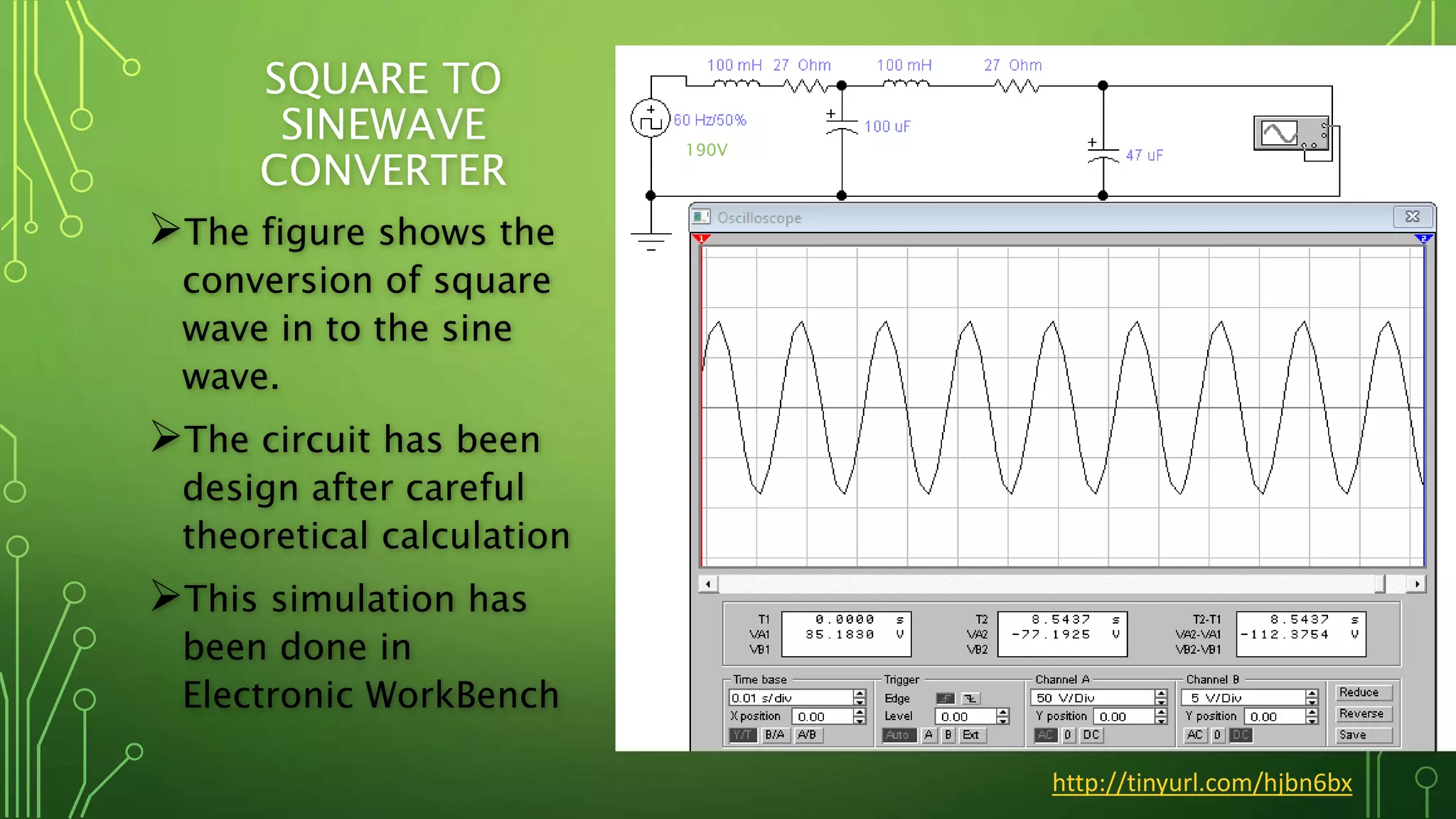
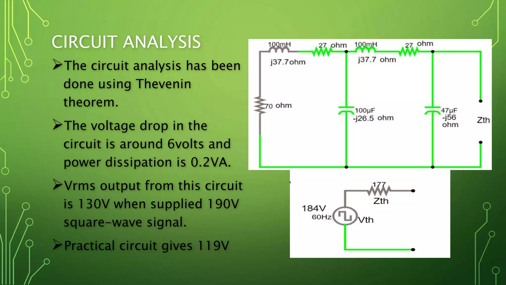
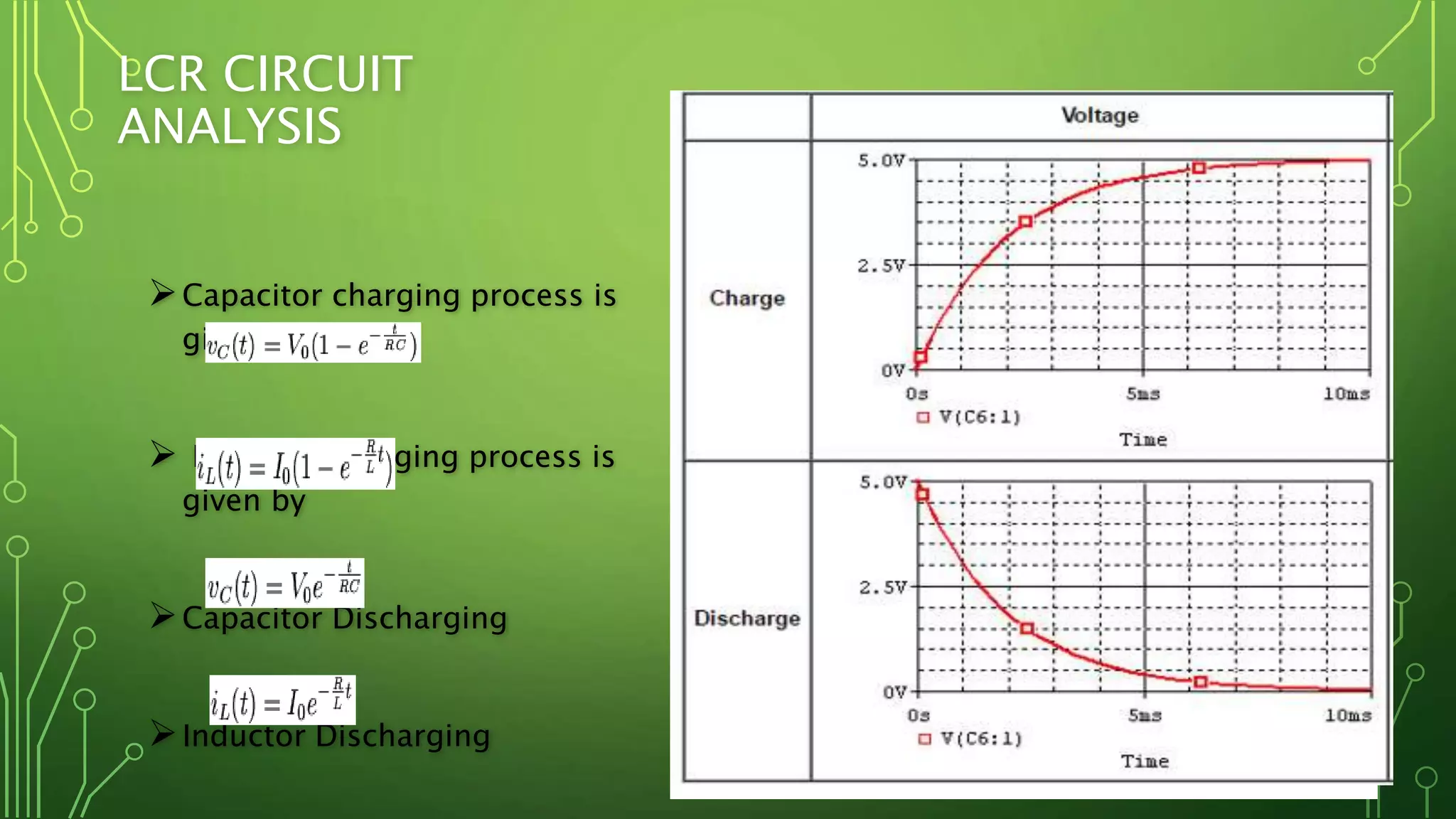
WELCOME TO THE OVERVIEW OF
INVERTER DESIGN PROJECT
SCHEMATIC CIRCUIT DESIGN IN AUTOCAD
BASIC PRINCIPLE OF INVERTER
State S1 S2 Output Voltage
1 + − +E
2 − − 0
3 − + −E
4 + + 0
ASTABLE
MULTIVIBRATOR
Duty Cycle (D) = Thigh/(Thigh + Tlow)= 50%
Output Frequency = 1/(Tlow + Thigh) =
1.44/((Ra + 2Rb) * C) = 60 Hz
RA = 3.3𝐾Ω , RB = 107.5𝐾Ω
& C = 0.11µF
SWITCHING CIRCUIT
When high signal comes from
oscillator it activates transistors
bringing it in forward biased.
As soon as the transistor saturated
the current flows from Collector to
emitter and works as switch on.
When input signal to the base is zero
the transistors are reversed biased
and there is no flow of current from
Collector to Emitter and hence the
switch is off.
STEP-UP
TRANSFORMER
Primary supply 12 –
0 – 12 Volts 2.5A
Square wave
Secondary output
123 Volts, 245mA
Square wave
Power rating 30VA
SQUARE TO
SINEWAVE
CONVERTER
The figure shows the
conversion of square
wave in to the sine
wave.
The circuit has been
design after careful
theoretical calculation
This simulation has
been done in
Electronic WorkBench
http://tinyurl.com/hjbn6bx
190V
CIRCUIT ANALYSIS
The circuit analysis has been
done using Thevenin
theorem.
The voltage drop in the
circuit is around 6volts and
power dissipation is 0.2VA.
Vrms output from this circuit
is 130V when supplied 190V
square-wave signal.
Practical circuit gives 119V
LCR CIRCUIT
ANALYSIS
Capacitor charging process is
given by
 Inductor Charging process is
given by
Capacitor Discharging
Inductor Discharging
A COMPLETE INVERTER CARD
http://tinyurl.com/k8y34xb
COMMERCIAL APPLICATION
Inverter is widely used every where in industrial,
household and official appliance for power back
devices.
Ac power is convenient for long distance power
transmission.
Power produced from windmill and solar panel
often saves in storage cell. Inverter is the primary
device for the conversion of the DC power into the
AC power.
CONT.……….
Continuous running motor and other signal processing
sophisticated devices need pure sine wave.
However, it is expensive pure sine wave generator often
installed as apart of an inverter.
sampling circuits, thyristor firing circuits, frequency generator
circuits, tone generator circuits etc. use triangular Wave
The inverter is widely used to the regions where power supply
interruption is frequent costumes.
CHALLENGES AND TROUBLESHOOTING
The power transistors heat quickly due to the
rapid switching. It is minimized by the help of heat
sink and current limiting resistors.
It is very difficult to design square wave using 555
timer however, 51% duty cycle is maintained.
The voltage drops drastically when converts
square wave to sine wave. The problem is figured
out but not implemented
Tolerance of components is the major factor in
the implementation of designed electronic circuit.
CONCLUSION
In spite of many problems encountered during
the designing of the project, almost all problems
are solved.
The theoretical and methodology parts are pretty
enough for upgrading high power sine wave
inverter
Lack of low resistance high current inductor and
high power CT transformer this project is limited
to low power supply.
THANK YOU
The end

Inverter design ppt

  • 1.
    WELCOME TO THEOVERVIEW OF INVERTER DESIGN PROJECT
  • 2.
  • 3.
    BASIC PRINCIPLE OFINVERTER State S1 S2 Output Voltage 1 + − +E 2 − − 0 3 − + −E 4 + + 0
  • 4.
    ASTABLE MULTIVIBRATOR Duty Cycle (D)= Thigh/(Thigh + Tlow)= 50% Output Frequency = 1/(Tlow + Thigh) = 1.44/((Ra + 2Rb) * C) = 60 Hz RA = 3.3𝐾Ω , RB = 107.5𝐾Ω & C = 0.11µF
  • 6.
    SWITCHING CIRCUIT When highsignal comes from oscillator it activates transistors bringing it in forward biased. As soon as the transistor saturated the current flows from Collector to emitter and works as switch on. When input signal to the base is zero the transistors are reversed biased and there is no flow of current from Collector to Emitter and hence the switch is off.
  • 7.
    STEP-UP TRANSFORMER Primary supply 12– 0 – 12 Volts 2.5A Square wave Secondary output 123 Volts, 245mA Square wave Power rating 30VA
  • 8.
    SQUARE TO SINEWAVE CONVERTER The figureshows the conversion of square wave in to the sine wave. The circuit has been design after careful theoretical calculation This simulation has been done in Electronic WorkBench http://tinyurl.com/hjbn6bx 190V
  • 10.
    CIRCUIT ANALYSIS The circuitanalysis has been done using Thevenin theorem. The voltage drop in the circuit is around 6volts and power dissipation is 0.2VA. Vrms output from this circuit is 130V when supplied 190V square-wave signal. Practical circuit gives 119V
  • 11.
    LCR CIRCUIT ANALYSIS Capacitor chargingprocess is given by  Inductor Charging process is given by Capacitor Discharging Inductor Discharging
  • 12.
  • 13.
  • 15.
    COMMERCIAL APPLICATION Inverter iswidely used every where in industrial, household and official appliance for power back devices. Ac power is convenient for long distance power transmission. Power produced from windmill and solar panel often saves in storage cell. Inverter is the primary device for the conversion of the DC power into the AC power.
  • 16.
    CONT.………. Continuous running motorand other signal processing sophisticated devices need pure sine wave. However, it is expensive pure sine wave generator often installed as apart of an inverter. sampling circuits, thyristor firing circuits, frequency generator circuits, tone generator circuits etc. use triangular Wave The inverter is widely used to the regions where power supply interruption is frequent costumes.
  • 17.
    CHALLENGES AND TROUBLESHOOTING Thepower transistors heat quickly due to the rapid switching. It is minimized by the help of heat sink and current limiting resistors. It is very difficult to design square wave using 555 timer however, 51% duty cycle is maintained. The voltage drops drastically when converts square wave to sine wave. The problem is figured out but not implemented Tolerance of components is the major factor in the implementation of designed electronic circuit.
  • 18.
    CONCLUSION In spite ofmany problems encountered during the designing of the project, almost all problems are solved. The theoretical and methodology parts are pretty enough for upgrading high power sine wave inverter Lack of low resistance high current inductor and high power CT transformer this project is limited to low power supply.
  • 19.