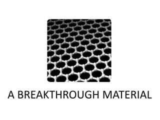
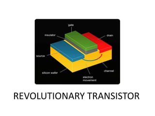
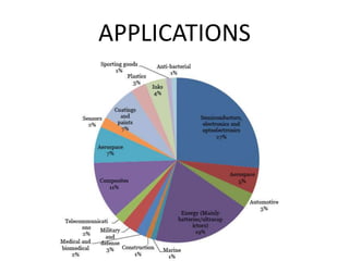
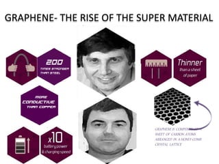
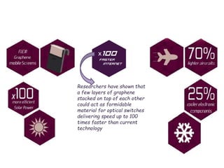
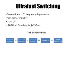
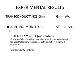
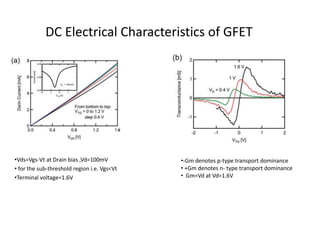
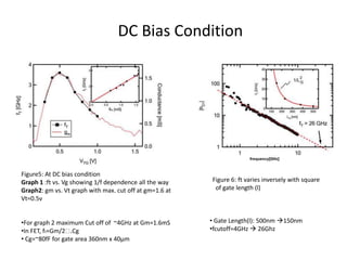
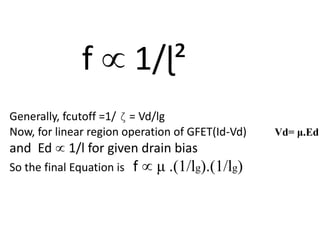
GRAPHENE
TRANSISTOR
19th September 2014
VSSUT, Burla
Shital Prasad Badaik
Reg. No-11010240
Section:ETC-2
Branch-E.T.C.E
A BREAKTHROUGH MATERIAL
REVOLUTIONARY TRANSISTOR
APPLICATIONS
“BREAKTHROUGH MATERIAL”
(Hint: It’s not Silicon)
GRAPHENE IS COMPOSED OF A
SHEET OF CARBON ATOMS
ARRANGED IN A HONEY-COMB
CRYSTAL LATTICE
GRAPHENE- THE RISE OF THE SUPER MATERIAL
Researchers have shown that
a few layers of graphene
stacked on top of each other
could act as formidable
material for optical switches
delivering speed up to 100
times faster than current
technology
FABRICATION TECHNIQUES
Ultrafast Switching
•Conventional 1/f frequency dependence
•high carrier mobility
•IGAIN  1/f
• 26GHz at Gate length(l)=150nm
THE EXPERIMENT:
Mechanical
exfoliation
Source and
drain (1nm)
12nm Al
(ALD),250ºC
TMA+NO2
Metal
deposition
EXPERIMENTAL RESULTS
TRANSCONDUCTANCE(Gm) Gm= Id/Vd
FIELD EFFECT MOBILITY(μ) ∆ =q. ∆n.
μ
μ= 400 cm2/V.s (estimated)
•Distortion in field mobility can mainly arise due to deposition of
Top Gate Dielectric which reduces both field effect mobility &
device Gm
•Charge impurity scattering
DC Electrical Characteristics of GFET
•Vds=Vgs-Vt at Drain bias ,Vd=100mV
• for the sub-threshold region i.e. Vgs<Vt
•Terminal voltage=1.6V
•-Gm denotes p-type transport dominance
• +Gm denotes n- type transport dominance
• Gm=Vd at Vd=1.6V
Fig(4a): h21=small signal current gain
h21= iD/iG
fig(4b): 1/f dependence of h21 and also
ft=h21xf for h21=1(figure of merit)
High Frequency Response Measurement of GFETs
(HP8510- vector network analyzer)
•AC current and Voltages are directly related by
scattering parameter for drain and source
• Open, Short and Load calibration employed to
network analyzer to de-embed signals to
calculate parasitic gate capacitance
•h21  1/f
•Ft= h21 x f (here ~4Ghz)
• -20dB slope for c. FET for Z=1/j.w.Cg
Figure5: At DC bias condition
Graph 1 :ft vs. Vg showing 1/f dependence all the way
Graph2: gm vs. Vt graph with max. cut off at gm=1.6 at
Vt=0.5v
•For graph 2 maximum Cut off of ~4GHz at Gm=1.6mS
•In FET, ft=Gm/2 .Cg
• Cg=~80fF for gate area 360nm x 40μm
Figure 6: ft varies inversely with square
of gate length (l)
DC Bias Condition
• Gate Length(l): 500nm 150nm
•fcutoff=4GHz  26Ghz
f  1/ɭ²
Generally, fcutoff =1/ ζ = Vd/lg
Now, for linear region operation of GFET(Id-Vd) Vd= μ.Ed
and Ed  1/l for given drain bias
So the final Equation is f  μ .(1/lg).(1/lg)
Effect of using Metal Contacts
Contact Induced Defect
•BAND ALTERATION: Charge transfer takes place from Co contact to source and drain
•In negative Gate region, anomaly in Transfer characteristics is reported
•Shift in Fermi level
• Diffusion of Co atoms into graphene channels
Skepticism of carrier mobility
Fig.1 Cross-section of N-channel Si
MOSFET
Fig.2 transfer Characteristics of Si
MOSFET
HIGH
FREQUENCY
OPERATION
CHANNEL
LENGTH
BAND GAP
CARRIER
MOBILITY
CONCLUSION
Versatile
properties
Leapfrog
applications
&
products
Engineering
Euphoria
References
1. Graphene Electronics: Materials, Devices, and Circuits by Yanqing Wu,
Damon B. Farmer, Fengnian Xia, and Phaedon Avouris
2. Graphene put down still decades to replace current Si-tech an article by
Joel Hruska
3. Operation of Graphene Transistors at GHz Frequencies by Yu-Ming Lin*,
Keith A. Jenkins, Alberto Valdes-Garcia, Joshua P. Small, Damon B.
Farmer, and Phaedon Avouris
4. Transfer Characteristics in Graphene Field-Effect Transistors with Co
Contacts by Ryo Nouchi, Masashi Shiraishi and Yoshishige Suzuki
5. Graphene-Fundamental and Emergent Applications by Jamie H. Warner,
Franziska Schaffel, Alicia Bachmatiuk, Mark H. Rummeli
6. Direct Growth of Graphene Film on Germanium Substrate by Gang
Wang, Miao Zhang, Yun Zhu, Guqiao Ding, Da Jiang, Qinglei Guo,Su Liu,
Xiaoming Xie, Paul K. Chu, Zengfeng Di & Xi Wang
7. Graphene transistors by Frank Schwierz, Nature Nanotechnology

Graphene Transistor By Shital Badaik

  • 1.
    GRAPHENE TRANSISTOR 19th September 2014 VSSUT,Burla Shital Prasad Badaik Reg. No-11010240 Section:ETC-2 Branch-E.T.C.E
  • 2.
  • 3.
  • 5.
  • 6.
  • 7.
    GRAPHENE IS COMPOSEDOF A SHEET OF CARBON ATOMS ARRANGED IN A HONEY-COMB CRYSTAL LATTICE GRAPHENE- THE RISE OF THE SUPER MATERIAL
  • 8.
    Researchers have shownthat a few layers of graphene stacked on top of each other could act as formidable material for optical switches delivering speed up to 100 times faster than current technology
  • 9.
  • 13.
    Ultrafast Switching •Conventional 1/ffrequency dependence •high carrier mobility •IGAIN  1/f • 26GHz at Gate length(l)=150nm THE EXPERIMENT: Mechanical exfoliation Source and drain (1nm) 12nm Al (ALD),250ºC TMA+NO2 Metal deposition
  • 15.
    EXPERIMENTAL RESULTS TRANSCONDUCTANCE(Gm) Gm=Id/Vd FIELD EFFECT MOBILITY(μ) ∆ =q. ∆n. μ μ= 400 cm2/V.s (estimated) •Distortion in field mobility can mainly arise due to deposition of Top Gate Dielectric which reduces both field effect mobility & device Gm •Charge impurity scattering
  • 16.
    DC Electrical Characteristicsof GFET •Vds=Vgs-Vt at Drain bias ,Vd=100mV • for the sub-threshold region i.e. Vgs<Vt •Terminal voltage=1.6V •-Gm denotes p-type transport dominance • +Gm denotes n- type transport dominance • Gm=Vd at Vd=1.6V
  • 17.
    Fig(4a): h21=small signalcurrent gain h21= iD/iG fig(4b): 1/f dependence of h21 and also ft=h21xf for h21=1(figure of merit) High Frequency Response Measurement of GFETs (HP8510- vector network analyzer) •AC current and Voltages are directly related by scattering parameter for drain and source • Open, Short and Load calibration employed to network analyzer to de-embed signals to calculate parasitic gate capacitance •h21  1/f •Ft= h21 x f (here ~4Ghz) • -20dB slope for c. FET for Z=1/j.w.Cg
  • 18.
    Figure5: At DCbias condition Graph 1 :ft vs. Vg showing 1/f dependence all the way Graph2: gm vs. Vt graph with max. cut off at gm=1.6 at Vt=0.5v •For graph 2 maximum Cut off of ~4GHz at Gm=1.6mS •In FET, ft=Gm/2 .Cg • Cg=~80fF for gate area 360nm x 40μm Figure 6: ft varies inversely with square of gate length (l) DC Bias Condition • Gate Length(l): 500nm 150nm •fcutoff=4GHz  26Ghz
  • 19.
    f  1/ɭ² Generally,fcutoff =1/ ζ = Vd/lg Now, for linear region operation of GFET(Id-Vd) Vd= μ.Ed and Ed  1/l for given drain bias So the final Equation is f  μ .(1/lg).(1/lg)
  • 20.
    Effect of usingMetal Contacts Contact Induced Defect •BAND ALTERATION: Charge transfer takes place from Co contact to source and drain •In negative Gate region, anomaly in Transfer characteristics is reported •Shift in Fermi level • Diffusion of Co atoms into graphene channels
  • 21.
    Skepticism of carriermobility Fig.1 Cross-section of N-channel Si MOSFET Fig.2 transfer Characteristics of Si MOSFET
  • 22.
  • 23.
  • 24.
    References 1. Graphene Electronics:Materials, Devices, and Circuits by Yanqing Wu, Damon B. Farmer, Fengnian Xia, and Phaedon Avouris 2. Graphene put down still decades to replace current Si-tech an article by Joel Hruska 3. Operation of Graphene Transistors at GHz Frequencies by Yu-Ming Lin*, Keith A. Jenkins, Alberto Valdes-Garcia, Joshua P. Small, Damon B. Farmer, and Phaedon Avouris 4. Transfer Characteristics in Graphene Field-Effect Transistors with Co Contacts by Ryo Nouchi, Masashi Shiraishi and Yoshishige Suzuki 5. Graphene-Fundamental and Emergent Applications by Jamie H. Warner, Franziska Schaffel, Alicia Bachmatiuk, Mark H. Rummeli 6. Direct Growth of Graphene Film on Germanium Substrate by Gang Wang, Miao Zhang, Yun Zhu, Guqiao Ding, Da Jiang, Qinglei Guo,Su Liu, Xiaoming Xie, Paul K. Chu, Zengfeng Di & Xi Wang 7. Graphene transistors by Frank Schwierz, Nature Nanotechnology