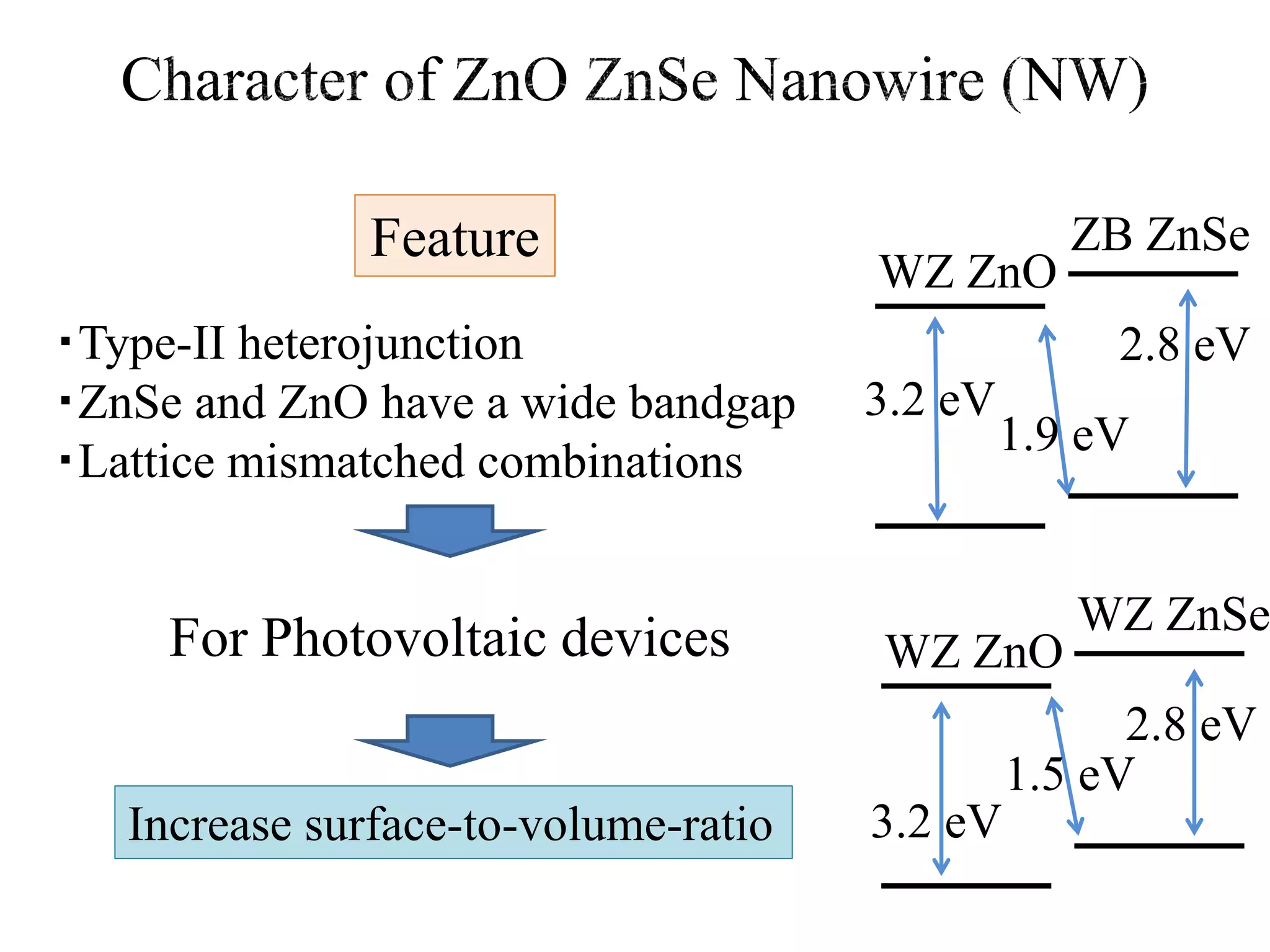
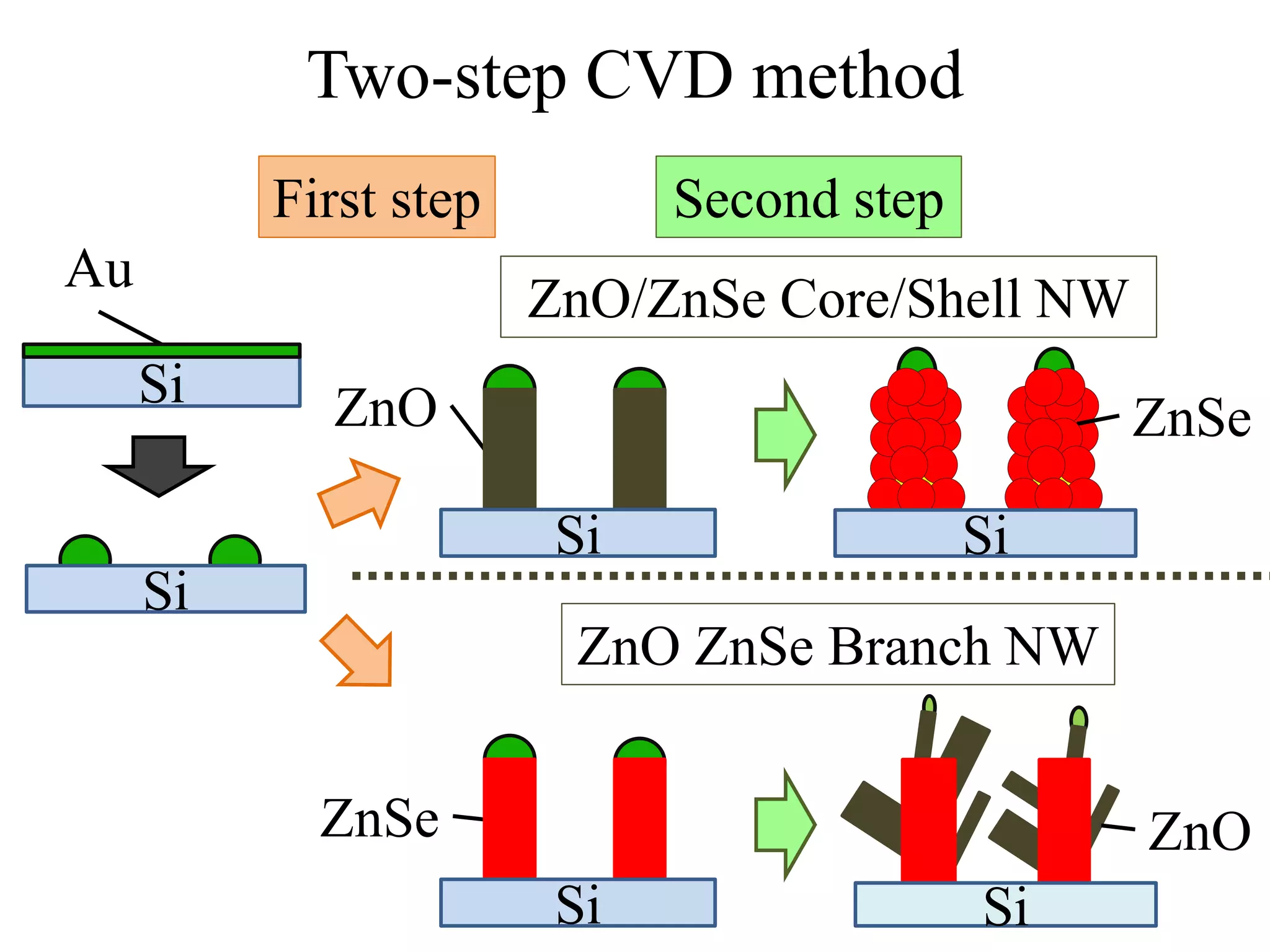
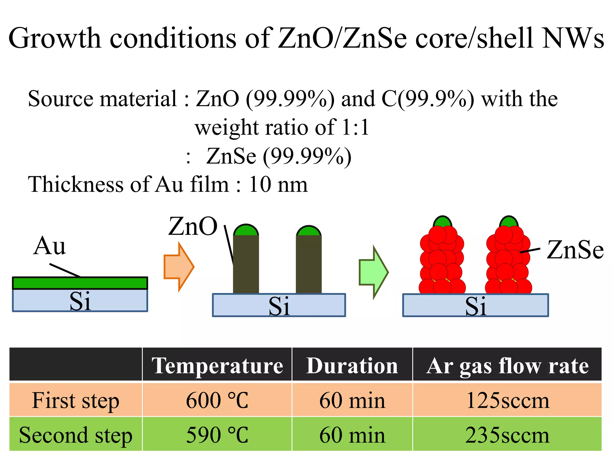
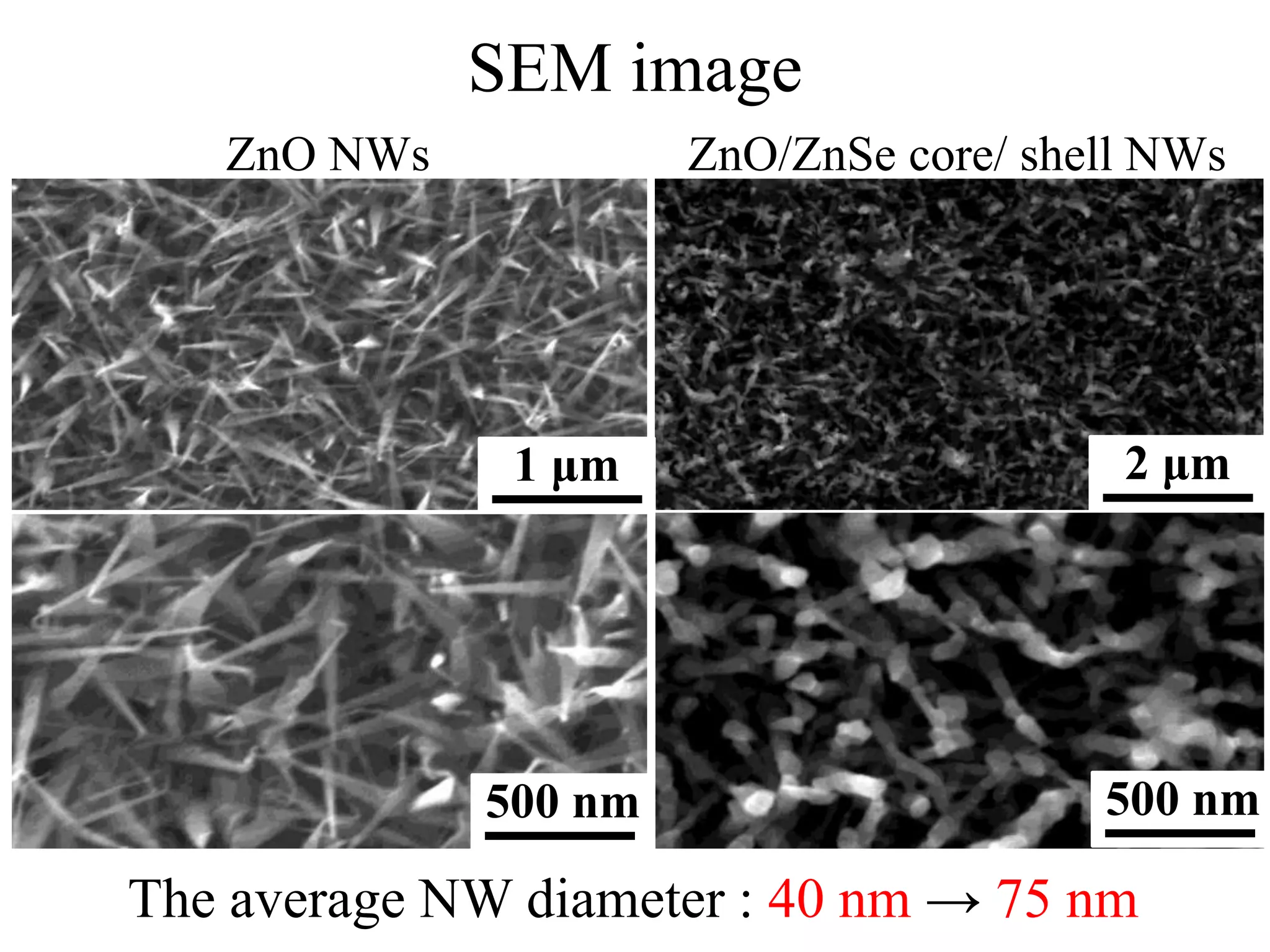
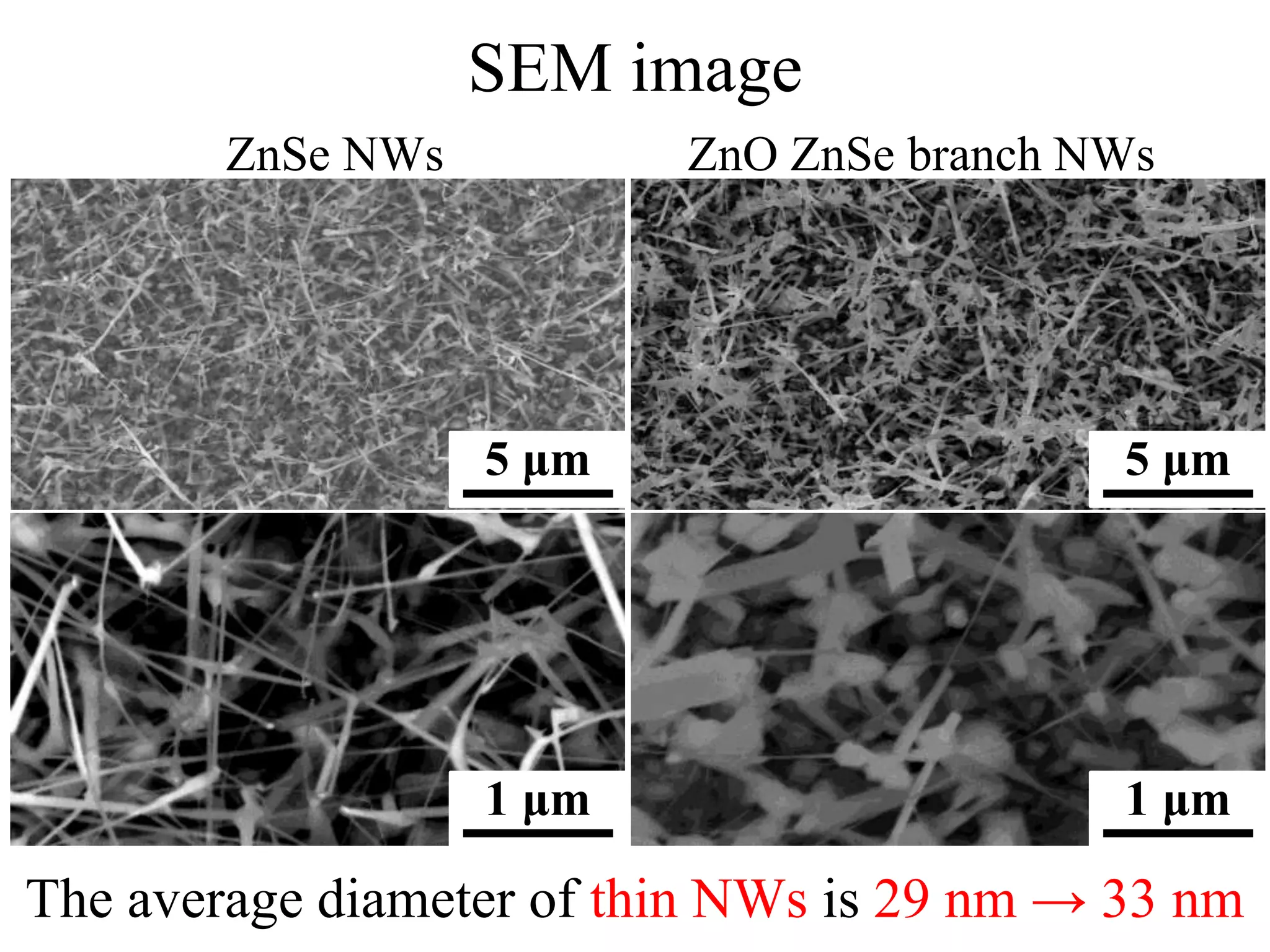
Growth of ZnO ZnSe nanowires
Yuya Sakamoto
WZ ZnO
ZB ZnSe
2.8 eV
3.2 eV
1.9 eV
Feature
・Type-II heterojunction
・ZnSe and ZnO have a wide bandgap
・Lattice mismatched combinations
WZ ZnO
WZ ZnSe
2.8 eV
3.2 eV
1.5 eV
For Photovoltaic devices
Increase surface-to-volume-ratio
Chemical Vapor Deposition (CVD) method
Quartz tube heater
Au on Si substrate ZnO/C or ZnSe
Ar Gas inletAr Gas outlet
0
200
400
600
800
1000
1200
0 10 20 30 40 50 60
Temperature[℃]
Position [cm]
Two-step CVD method
Au
Si ZnO
Si
First step Second step
ZnSe
Si
ZnSe
Si
ZnO
Si
ZnO/ZnSe Core/Shell NW
ZnO ZnSe Branch NW
Si
Growth conditions of ZnO/ZnSe core/shell NWs
Au
Si
ZnO
Si
ZnSe
Si
Temperature Duration Ar gas flow rate
First step 600 ℃ 60 min 125sccm
Second step 590 ℃ 60 min 235sccm
Source material : ZnO (99.99%) and C(99.9%) with the
weight ratio of 1:1
: ZnSe (99.99%)
Thickness of Au film : 10 nm
SEM image
ZnO NWs ZnO/ZnSe core/ shell NWs
The average NW diameter : 40 nm → 75 nm
500 nm 500 nm
1 μm 2 μm
EDX spectrum
The diameter correspond to ZnO/ZnSe core/shell NW
0
50
100
150
200
250
300
0 20 40 60 80 100 120 140 160 180 200
Intensity[a.u.]
Distance [nm]
1 μm
90 nm
120 nm
Photoluminescence Spectrum
ZnO Bandedge (BE) emission : 380 nm = 3.26 eV
ZnSe BE emission : 460 nm = 2.69 eV
ZnSe Deep Level (DL) emission: 640 nm = 1.93 eV
Laser wavelength : 361.2 nm
Room temperature
Growth conditions of ZnO ZnSe branch NWs
Au
Si
Temperatu𝐫𝐞 Duration Ar gas flow rate
First step 640 ℃ 60 min 235sccm
Second step 590 ℃ 60 min 125sccm
ZnSe
Si
ZnO
Si
Source material : ZnO (99.99%) and C(99.9%) with the
weight ratio of 1:1
ZnSe (99.99%)
Thickness of Au film : 10 nm
SEM image
ZnSe NWs ZnO ZnSe branch NWs
The average diameter of thin NWs is 29 nm → 33 nm
5 μm 5 μm
1 μm 1 μm
0
100
200
300
400
0 50 100 150 200 250 300
Intensity[a.u.]
Distance [nm]
0
50
100
150
200
0 30 60 90 120 150 180
Intensity[a.u.] Distance [nm]
ZnO ZnSe branch NW data by EDX line profile
2
1 1
2
1 μm
PL
ZnSe BE emission : 442 nm = 2.8 eV
ZnSe DL emission : 640 nm = 1.9 eV
ZnO BE emission : 380 nm =3.26 eV
Laser wavelength : 361.2 nm
Room temperature
・ Characterize the ZnO/ZnSe core/shell NWs and ZnO ZnSe branch NW
by XRD and PL
・ Observe the surface morphology of ZnO/ZnSe core/shell NW, and ZnO
ZnSe branch heterostructure NW by SEM
・ Found the conditions for growth ZnO/ZnSe core/shell heterostructure
NW, and ZnO ZnSe branch heterostructure NW
Future Work
・ Measure the electrical property by Electron beam induced current
・ Fabricate the single NW device with ZnO ZnSe branch structure NW
by electron beam lithography
・ Upgrade the quality of ZnO and ZnSe NWs before growth second
material
・ Measure the junction of ZnO and ZnSe by transmission electron
microscopy to confirm ZnO NWs are connecting to ZnSe NWs
Acknowledgement
・ I would like to express my deep gratitude to Professor Harry E. Ruda,
for his patient guidance and useful critiques of this research work.
・ I would also like to thank Dr. Carlos Fernandes, for his advice and
assistance in keeping my progress on schedule.
・ I would also like to thank Dr Souza Christina and Dave Wisnieski for
measuring PL spectrum and teaching me how to analyze spectrum.
・ I wish to express my sincere gratitude to all of the concerned people,
who help me to finish my all procedure, correct my English, promote my
experiments.
Laser reference
330 360 390
0
2000
4000
6000
Intensity(arb.unit)
Wavelength (nm)
Leaser reference
Analysis
The mean diameter of base : 223 nm
The mean diameter of branch : 52 nm
The diameter of ZnO was also almost 40 nm
ZnSe : June 28
ZnO : July 4
ZnO ZnSe branch NW data by EDX line profile
①
②
②
①
There is the ZnSe ZnO hetero structure NW
My opinion
I measured 20 NWs by ESM and EDX. The compositions of thin NWs were ZnSe
ZnO NWs weren’t grown on ZnSe NWs
ZnO
Au
ZnSe
Before using EDX,
I guessed this structure
ZnO
ZnSe
After using EDX, I believe it was happened in the furnace
∆𝐸 + ∆𝐸 =

Conclusion of the experiment in canada!

  • 1.
    Growth of ZnOZnSe nanowires Yuya Sakamoto
  • 2.
    WZ ZnO ZB ZnSe 2.8eV 3.2 eV 1.9 eV Feature ・Type-II heterojunction ・ZnSe and ZnO have a wide bandgap ・Lattice mismatched combinations WZ ZnO WZ ZnSe 2.8 eV 3.2 eV 1.5 eV For Photovoltaic devices Increase surface-to-volume-ratio
  • 3.
    Chemical Vapor Deposition(CVD) method Quartz tube heater Au on Si substrate ZnO/C or ZnSe Ar Gas inletAr Gas outlet 0 200 400 600 800 1000 1200 0 10 20 30 40 50 60 Temperature[℃] Position [cm]
  • 4.
    Two-step CVD method Au SiZnO Si First step Second step ZnSe Si ZnSe Si ZnO Si ZnO/ZnSe Core/Shell NW ZnO ZnSe Branch NW Si
  • 5.
    Growth conditions ofZnO/ZnSe core/shell NWs Au Si ZnO Si ZnSe Si Temperature Duration Ar gas flow rate First step 600 ℃ 60 min 125sccm Second step 590 ℃ 60 min 235sccm Source material : ZnO (99.99%) and C(99.9%) with the weight ratio of 1:1 : ZnSe (99.99%) Thickness of Au film : 10 nm
  • 6.
    SEM image ZnO NWsZnO/ZnSe core/ shell NWs The average NW diameter : 40 nm → 75 nm 500 nm 500 nm 1 μm 2 μm
  • 7.
    EDX spectrum The diametercorrespond to ZnO/ZnSe core/shell NW 0 50 100 150 200 250 300 0 20 40 60 80 100 120 140 160 180 200 Intensity[a.u.] Distance [nm] 1 μm 90 nm 120 nm
  • 8.
    Photoluminescence Spectrum ZnO Bandedge(BE) emission : 380 nm = 3.26 eV ZnSe BE emission : 460 nm = 2.69 eV ZnSe Deep Level (DL) emission: 640 nm = 1.93 eV Laser wavelength : 361.2 nm Room temperature
  • 9.
    Growth conditions ofZnO ZnSe branch NWs Au Si Temperatu𝐫𝐞 Duration Ar gas flow rate First step 640 ℃ 60 min 235sccm Second step 590 ℃ 60 min 125sccm ZnSe Si ZnO Si Source material : ZnO (99.99%) and C(99.9%) with the weight ratio of 1:1 ZnSe (99.99%) Thickness of Au film : 10 nm
  • 10.
    SEM image ZnSe NWsZnO ZnSe branch NWs The average diameter of thin NWs is 29 nm → 33 nm 5 μm 5 μm 1 μm 1 μm
  • 11.
    0 100 200 300 400 0 50 100150 200 250 300 Intensity[a.u.] Distance [nm] 0 50 100 150 200 0 30 60 90 120 150 180 Intensity[a.u.] Distance [nm] ZnO ZnSe branch NW data by EDX line profile 2 1 1 2 1 μm
  • 12.
    PL ZnSe BE emission: 442 nm = 2.8 eV ZnSe DL emission : 640 nm = 1.9 eV ZnO BE emission : 380 nm =3.26 eV Laser wavelength : 361.2 nm Room temperature
  • 13.
    ・ Characterize theZnO/ZnSe core/shell NWs and ZnO ZnSe branch NW by XRD and PL ・ Observe the surface morphology of ZnO/ZnSe core/shell NW, and ZnO ZnSe branch heterostructure NW by SEM ・ Found the conditions for growth ZnO/ZnSe core/shell heterostructure NW, and ZnO ZnSe branch heterostructure NW
  • 14.
    Future Work ・ Measurethe electrical property by Electron beam induced current ・ Fabricate the single NW device with ZnO ZnSe branch structure NW by electron beam lithography ・ Upgrade the quality of ZnO and ZnSe NWs before growth second material ・ Measure the junction of ZnO and ZnSe by transmission electron microscopy to confirm ZnO NWs are connecting to ZnSe NWs
  • 15.
    Acknowledgement ・ I wouldlike to express my deep gratitude to Professor Harry E. Ruda, for his patient guidance and useful critiques of this research work. ・ I would also like to thank Dr. Carlos Fernandes, for his advice and assistance in keeping my progress on schedule. ・ I would also like to thank Dr Souza Christina and Dave Wisnieski for measuring PL spectrum and teaching me how to analyze spectrum. ・ I wish to express my sincere gratitude to all of the concerned people, who help me to finish my all procedure, correct my English, promote my experiments.
  • 16.
    Laser reference 330 360390 0 2000 4000 6000 Intensity(arb.unit) Wavelength (nm) Leaser reference
  • 17.
    Analysis The mean diameterof base : 223 nm The mean diameter of branch : 52 nm The diameter of ZnO was also almost 40 nm
  • 18.
    ZnSe : June28 ZnO : July 4 ZnO ZnSe branch NW data by EDX line profile ① ② ② ① There is the ZnSe ZnO hetero structure NW
  • 19.
    My opinion I measured20 NWs by ESM and EDX. The compositions of thin NWs were ZnSe ZnO NWs weren’t grown on ZnSe NWs ZnO Au ZnSe Before using EDX, I guessed this structure ZnO ZnSe After using EDX, I believe it was happened in the furnace
  • 22.

Editor's Notes

  • #3 Type Ⅱ heterojunction Bandgap diagram National Renewable Energy Laboratory 格子ミスマッチ→キャリア伝導に寄与
  • #4 To grow the NW, I use a chemical vapor deposition method. Before growth NWs, As preparation of Au deposition , I prepare Si substrates, which is (100) p-type, and clean up the surface and get rid of the oxide layer using Aseton, IPA, DI water, and Hydrofluoric, and then deposit 10 nm Au film on the Si substrate by a thermal evaporation method. Au help growth of NWs as a catalyst. そして、Ar gas を流す。Ar gus was introduced into the tube. I use a two steps chemical vapor deposition method
  • #6 In the first step, I prepared source materials of ZnO and C with mass ration of 1 to 1. I deposit the 10 nm of the Au film on the Si substrate, as the catalyst. the ZnSe films were prepared by vacuum evaporation method under the pressure better than 10-5 Torr on chemically cleaned glass substrates from 99.99% pure ZnSe powder (Aldrich) using molybdenum boat.
  • #7 右上 top right Look at the bottom two pictures The SEM images on the left side is before growing ZnSe NWs, right side is after growing ZnO NWs on the ZnSe NWs
  • #9 This is the PL spectrum data from ZnO and ZnO/ZnSe core/shell NWs. Basically, There is a ZnSe DL emission. As shown in enlarged figure, There is a slightly ZnO BE emission.
  • #11 The top Left and the top right are the same magnification. The bottom ones as well.
  • #13 There is the BE emission, also the strong DL emission observed
  • #16 I’d like to thank you (for 〜)
  • #20 I measure the Reduction of source materials each time