Downloaded 19 times

![<3>
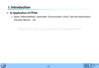
I. Introduction
1) What is FPGA?
Definition : Field Programmable Gate Array
→ Contain logical-gate (AND, OR, XOR, NOT… etc.), Flip-flop, and internal wire
→ “Programmable” during operating time and “Reconfigurable”
→ Cost-efficient, and flexible device
[Configuration of FPGA] [CMOS gate array of FPGA]](https://image.slidesharecdn.com/20171104ubuntu-171108035839/85/FPGA-4-320.jpg)
![<4>
I. Introduction
1) What is FPGA?
[ALTERA FPGA : Stratix IV] [Xilinx FPGA : KINTEX]](https://image.slidesharecdn.com/20171104ubuntu-171108035839/85/FPGA-5-320.jpg)
![<5>
I. Introduction
1) What is FPGA?
Main vendor : ALTERA, Xilinx, ACTEL, Mircrosemi, Lettice semiconductor …
IDE(Integrated Development Environment) : ATLERA Quartus, Xilinx ISE, Vivado,
ACTEL Libero …
HDL (Hardware Description Language) : VHDL, Verilog, System Verlilog … etc
→ Compatible each other
[ALTERA Quartus II] [Xilinx Vivado]](https://image.slidesharecdn.com/20171104ubuntu-171108035839/85/FPGA-6-320.jpg)
![<6>
I. Introduction
2) Development process
[FPGA Development Process]](https://image.slidesharecdn.com/20171104ubuntu-171108035839/85/FPGA-7-320.jpg)
![<7>
I. Introduction
2) Development process
[HDL Synthesis]](https://image.slidesharecdn.com/20171104ubuntu-171108035839/85/FPGA-8-320.jpg)
![<8>
I. Introduction
3) Difference between FPGA and DSP/MCU
[Difference between parallel process and sequential process]](https://image.slidesharecdn.com/20171104ubuntu-171108035839/85/FPGA-9-320.jpg)
![<11>
II. Trouble of developing FPGA
1) Timing violation due to negative slack
Slack : (Required clock period) – (Actual clock period)
Positive slack : The timing requirements are met
Negative slack : The timing requirements are not met
[Timing slack]](https://image.slidesharecdn.com/20171104ubuntu-171108035839/85/FPGA-12-320.jpg)
![<12>
II. Trouble of developing FPGA
1) Timing violation due to negative slack
As the master clock (60MHz) has the negative slack, the reset of 12bit free-
running counter causes some trouble
→ Negative slack is because of heavy encryption logic supported by supervisor corp
always @(posedge i_clk, negedge i_rstn) begin
if (!i_rstn) begin
cnt <= 12’d0;
end
else begin
cnt <= cnt + 1’d1;
end
end
[Free running counter logic]](https://image.slidesharecdn.com/20171104ubuntu-171108035839/85/FPGA-13-320.jpg)
![<14>
II. Trouble of developing FPGA
3) DDR3 I/F problem due to h/w design fault
[DDR3 SDRAM architecture and memory topology]](https://image.slidesharecdn.com/20171104ubuntu-171108035839/85/FPGA-15-320.jpg)
![<15>
II. Trouble of developing FPGA
3) DDR3 I/F problem due to h/w design fault
[DDR3 SDRAM controller block diagram]](https://image.slidesharecdn.com/20171104ubuntu-171108035839/85/FPGA-16-320.jpg)
![<16>
II. Trouble of developing FPGA
3) DDR3 I/F problem due to h/w design fault
[DDR3 SDRAM Write/Read process] [DDR3 SDRAM controller main FSM]](https://image.slidesharecdn.com/20171104ubuntu-171108035839/85/FPGA-17-320.jpg)
![<17>
II. Trouble of developing FPGA
3) DDR3 I/F problem due to h/w design fault
The clock frequency of DDR3 SDRAM is very high (1066 MHz)
→ Deliberate h/w design is required for DDR3 SDRAM control
: Impedance matching, PCB pattern routing, PCB pattern length and width… etc
→ Some H/W design fault causes DDR3 SRRAM control fault
[DDR3 SDRAM impedance matching]](https://image.slidesharecdn.com/20171104ubuntu-171108035839/85/FPGA-18-320.jpg)
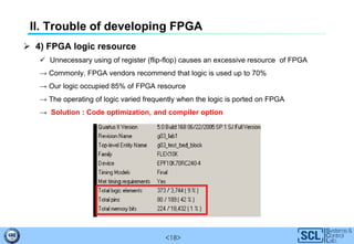


This document summarizes common issues encountered when developing FPGA projects. It introduces FPGAs, the development process, and applications. Key issues discussed include timing violations from negative slack, hardware configuration errors affecting ADCs, DDR3 interface problems from hardware design faults like improper impedance matching, and excessive resource usage from unnecessary registers. Solutions involve optimizing code and hardware design, as well as adjusting compiler options.