Passive Air Cooling System and Solar Water Heater.ppt
Experiment full.docx
1. Prepared By ASIF ULLAH KHAN
Electrical Technology, University of Technology, Nowshera. asifjan5942@gmail.com
Page 1
Digital Electronics Lab Manual
Experiment No 01
“Familiarization with Digital Electronics”
Digital Electronics
Digital electronics is a field of electronics involving the study of digital signals (binary
0, 1) and the engineering of devices that use or produce them.
The binary number system was refined by Gottfried wihelm
Leibniz (published 1705).
Boolean algebra is a division of mathematics that deals with operations
on (logical values) and incorporates /includes binary values / variables.
Boolean values are (0, 1).
Gates are made up of transistor, diodes and resistor.
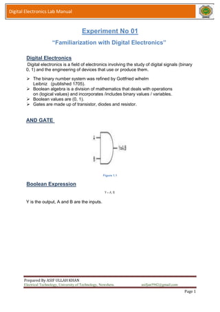
AND GATE
Figure 1.1
Boolean Expression
Y = A. B
Y is the output, A and B are the inputs.
2. Prepared By ASIF ULLAH KHAN
Electrical Technology, University of Technology, Nowshera. asifjan5942@gmail.com
Page 2
Digital Electronics Lab Manual
Diode Logic AND Gate
Figure 1.2
Proteus Simulations
Figure 1.3
3. Prepared By ASIF ULLAH KHAN
Electrical Technology, University of Technology, Nowshera. asifjan5942@gmail.com
Page 3
Digital Electronics Lab Manual
Truth Table
Input A Input B OUTPUT Y
0V 0V 0V
0V 5V 0V
5V 0V 0V
5V 5V 5V
Table 1.1
NOT GATE
Electrical Symbol
Figure 1.4
Boolean Expression
Y = A’
Y is the output, A is the input.
4. Prepared By ASIF ULLAH KHAN
Electrical Technology, University of Technology, Nowshera. asifjan5942@gmail.com
Page 4
Digital Electronics Lab Manual
Proteus Simulations
Figure 1.5
Truth Table
Input A Output Y
0V 5V
5V 0V
Table 1.2
Integrated circuit (I’c)
An electronic circuit formed on a small piece of semiconducting material which
performs the same function as a larger circuit made from discrete components.
5. Prepared By ASIF ULLAH KHAN
Electrical Technology, University of Technology, Nowshera. asifjan5942@gmail.com
Page 5
Digital Electronics Lab Manual
Classification of (IC’s)
S.No (IC’s) Classification No. Of Transistor No. Of Gate
1 Small scale Integration 10 – 100 3 - 30
2 Medium scale Integration 100 - 1000 30 - 300
3 Large scale Integration 1000 - 20000 300 – 3000
4 Very large scale Integration 20k – 50k Above 3000
5 Ultra large scale Integration 50k – 1billon >3000
___________________________________________________________________
6. Prepared By ASIF ULLAH KHAN
Electrical Technology, University of Technology, Nowshera. asifjan5942@gmail.com
Page 6
Digital Electronics Lab Manual
Experiment No 02
“To demonstrate diode logic AND and OR Gate”
Apparatus
1. Bread board.
2. Power supply.
3. Multimeter.
4. Resistor 2.2 kΩ.
5. Diode IN 4001.
6. Connecting leads.
Diode Logic AND Gate
Figure 2.1
Procedure
Implement the circuit on bread board as shown in figure for AND gate.
Apply voltage levels mentioned in the table on the inputs turn by turn and
measure the respective output voltage level at the output.
Record your observation in the table.
7. Prepared By ASIF ULLAH KHAN
Electrical Technology, University of Technology, Nowshera. asifjan5942@gmail.com
Page 7
Digital Electronics Lab Manual
Truth Table
Input A INPUT B OUTPUT Y
0V 0V 0V
0V 5V 0V
5V 0V 0V
5V 5V 5V
Table 2.1
Proteus Simulations
Figure 2.2
8. Prepared By ASIF ULLAH KHAN
Electrical Technology, University of Technology, Nowshera. asifjan5942@gmail.com
Page 8
Digital Electronics Lab Manual
Diode Logic OR Gate
Figure 2.3
Procedure
Implement the circuit on bread board as shown in figure for OR gate.
Apply voltage levels mentioned in the table on the inputs turn by turn and
measure the respective output voltage level at the output.
Record your observation in the table.
Truth Table
Input A INPUT B OUTPUT Y
0V 0V 0V
0V 5V 5V
5V 0V 5V
5V 5V 5V
Table 2.2
9. Prepared By ASIF ULLAH KHAN
Electrical Technology, University of Technology, Nowshera. asifjan5942@gmail.com
Page 9
Digital Electronics Lab Manual
Proteus Simulations
Figure 2.4
___________________________________________________________________
10. Prepared By ASIF ULLAH KHAN
Electrical Technology, University of Technology, Nowshera. asifjan5942@gmail.com
Page 10
Digital Electronics Lab Manual
Experiment No 03
“VERIFICATION OF TRUTH TABLE OF AND, OR, NOT,
NAND & NOR LOGIC GATES”
Apparatus
1) Supply (VDC=5V).
2) Ground.
3) LED.
4) SWITCH.
5) AND gate.
6) OR gate.
7) NOT gate.
8) NAND gate.
9) NOR gate.
Procedure
1. Open Proteus Professional Software.
2. Open New Project/Schematic.
3. Pick DC source from generator mode.
4. Pick desired Gates from component mode.
5. Pick Ground from terminal mode.
6. Pick LED from component mode.
7. Pick Switch from component mode.
8. Run the simulation.
AND GATE
Electrical Symbol
Figure 3.1
Boolean Expression
Y = A. B
Y is the output, A and B are the inputs.
11. Prepared By ASIF ULLAH KHAN
Electrical Technology, University of Technology, Nowshera. asifjan5942@gmail.com
Page 11
Digital Electronics Lab Manual
Truth Table
Protues Simulations
Figure 3.2
o
OR GATE
Electrical Symbol
Figure 3.3
INPUT A INPUT B OUTPUT Y
0V 0V 0V
0V 5V 0V
5V 0V 0V
5V 5V 5V
Table 3.1
12. Prepared By ASIF ULLAH KHAN
Electrical Technology, University of Technology, Nowshera. asifjan5942@gmail.com
Page 12
Digital Electronics Lab Manual
Boolean Expression
Y = A + B
Y is the output, A and B are the inputs.
Truth Table
Proteus Simulations
Figure 3.4
INPUT A INPUT B OUTPUT Y
0V 0V 0V
0V 5V 5V
5V 0V 5V
5V 5V 5V
Table 3.2
13. Prepared By ASIF ULLAH KHAN
Electrical Technology, University of Technology, Nowshera. asifjan5942@gmail.com
Page 13
Digital Electronics Lab Manual
NOT GATE
Electrical Symbol
Figure 3.5
Boolean Expression
A = Y
Y is the output, A is the input.
Truth Table
Proteus Simulations
Figure 3.6
INPUT A OUTPUT Y
0V 5V
5V 0V
Table 3.3
14. Prepared By ASIF ULLAH KHAN
Electrical Technology, University of Technology, Nowshera. asifjan5942@gmail.com
Page 14
Digital Electronics Lab Manual
NAND GATE
Electrical Symbol
Figure 3.7
Boolean Expression
Y = A. B
Y is the output, A and B are the inputs.
Truth Table
Proteus Simulations
INPUT A INPUT B OUTPUT Y
0V 0V 5V
0V 5V 5V
5V 0V 5V
5V 5V 0V
Table 3.4
15. Prepared By ASIF ULLAH KHAN
Electrical Technology, University of Technology, Nowshera. asifjan5942@gmail.com
Page 15
Digital Electronics Lab Manual
Figure 3.8
Home Task
NOR GATE
Electrical Symbol
Figure 3.9
Boolean Expression
Y = A + B
Y is the output, A and B are the inputs.
Truth Table
16. Prepared By ASIF ULLAH KHAN
Electrical Technology, University of Technology, Nowshera. asifjan5942@gmail.com
Page 16
Digital Electronics Lab Manual
Proteus Simulations
Figure 3.10
XOR GATE
Electrical Symbol
INPUT A INPUT B OUTPUT Y
0V 0V 5V
0V 5V 0V
5V 0V 0V
5V 5V 0V
Table 3.5
17. Prepared By ASIF ULLAH KHAN
Electrical Technology, University of Technology, Nowshera. asifjan5942@gmail.com
Page 17
Digital Electronics Lab Manual
Figure 3.11
Boolean Expression
Y is the output, A and B are the inputs.
Truth Table
Proteus Simulations
INPUT A INPUT B
OUTPUT Y
0V 0V 0V
0V 5V 5V
5V 0V 5V
5V 5V 0V
Table 3.6
18. Prepared By ASIF ULLAH KHAN
Electrical Technology, University of Technology, Nowshera. asifjan5942@gmail.com
Page 18
Digital Electronics Lab Manual
Figure 3.12
XNOR GATE
Electrical Symbol
Figure 3.13
Boolean Expression
19. Prepared By ASIF ULLAH KHAN
Electrical Technology, University of Technology, Nowshera. asifjan5942@gmail.com
Page 19
Digital Electronics Lab Manual
Y is the output, A and B are the inputs.
Truth Table
Proteus Simulations
INPUT A INPUT B
OUTPUT Y
0V 0V 5V
0V 5V 0V
5V 0V 0V
5V 5V 5V
Table 3.7
20. Prepared By ASIF ULLAH KHAN
Electrical Technology, University of Technology, Nowshera. asifjan5942@gmail.com
Page 20
Digital Electronics Lab Manual
Figure 3.14
___________________________________________________________________
21. Prepared By ASIF ULLAH KHAN
Electrical Technology, University of Technology, Nowshera. asifjan5942@gmail.com
Page 21
Digital Electronics Lab Manual
Experiment No 04
“Implementation of multivariable Boolean expression using
logic gates and Verification of DE Morgan’s Law”
Apparatus
1. 7408.
2. 7432.
3. 7404.
4. Connecting leads.
5. Digital Logic kit.
Given Boolean Function is;
F1 = a b’ c + a’ b c
F2 = (a + b+ c’) (a’ + b)
22. Prepared By ASIF ULLAH KHAN
Electrical Technology, University of Technology, Nowshera. asifjan5942@gmail.com
Page 22
Digital Electronics Lab Manual
Truth Table
Inputs Outputs
a b c x y F1
0 0 0 0 0 0
0 0 1 0 0 0
0 1 0 0 0 0
0 1 1 0 1 1
1 0 0 0 0 0
1 0 1 1 0 1
1 1 0 0 0 0
1 1 1 0 0 0
Table 4.1
23. Prepared By ASIF ULLAH KHAN
Electrical Technology, University of Technology, Nowshera. asifjan5942@gmail.com
Page 23
Digital Electronics Lab Manual
Proteus Simulations
1.
Figure 4.1
2.
Figure 4.2
24. Prepared By ASIF ULLAH KHAN
Electrical Technology, University of Technology, Nowshera. asifjan5942@gmail.com
Page 24
Digital Electronics Lab Manual
3.
Figure 4.3
_______________________________________________________________________________________________________
Home Task
Truth Table
Inputs Outputs
a b c x y F1
0 0 0 1 1 1
0 0 1 0 1 0
0 1 0 1 1 1
0 1 1 1 1 1
26. Prepared By ASIF ULLAH KHAN
Electrical Technology, University of Technology, Nowshera. asifjan5942@gmail.com
Page 26
Digital Electronics Lab Manual
2.
Figure 4.5
3.
Figure 4.6
_______________________________________________________________________________________________________
27. Prepared By ASIF ULLAH KHAN
Electrical Technology, University of Technology, Nowshera. asifjan5942@gmail.com
Page 27
Digital Electronics Lab Manual
“DE Morgan’s Law”
APPARATUS
1. 7408.
2. 7432.
3. 7404.
4. Connecting leads.
5. Digital Logic kit.
DE Morgan’s Law
It has two statements.
(x+y)’ = x’. y’
Where let F1 = (x+y)’ & F2 = x’. y’
(x.y)’ = x’+ y’
Where let F3 = (x.y)’ & F4 = x’+ y’
28. Prepared By ASIF ULLAH KHAN
Electrical Technology, University of Technology, Nowshera. asifjan5942@gmail.com
Page 28
Digital Electronics Lab Manual
Truth Table
Inputs Outputs
X Y F1 = (x+y)’ F2 = x’. y’ F3 = (x.y)’ F4 =x’+ y’
0 0 1 1 1 1
0 1 0 0 1 1
1 0 0 0 1 1
1 1 0 0 0 0
Table 4.3
Proteus Simulations
1.
Figure 4.7
29. Prepared By ASIF ULLAH KHAN
Electrical Technology, University of Technology, Nowshera. asifjan5942@gmail.com
Page 29
Digital Electronics Lab Manual
2.
Figure 4.8
________________________________________________________________________________________________________
30. Prepared By ASIF ULLAH KHAN
Electrical Technology, University of Technology, Nowshera. asifjan5942@gmail.com
Page 30
Digital Electronics Lab Manual
Home Task
(x+y+z)’ = x’ .y’ .z’
Where let F1 = (x+y+z)’ & F2 = x’ .y’ .z’
(x.y.z)’ = x’ +y’ +z’
Where let F3 (x.y.z)’ & F4 = x’ +y’ +z’
31. Prepared By ASIF ULLAH KHAN
Electrical Technology, University of Technology, Nowshera. asifjan5942@gmail.com
Page 31
Digital Electronics Lab Manual
Truth Table
Inputs Outputs
X Y Z
F1 = (x+y+z)’ F2 = x’ .y’ .z’
Actual Observed Actual Observed
1 1 1 1
0 0 0 0 0 0 0
0 0 1 0 0 0 0
0 1 0 0 0 0 0
0 1 1 0 0 0 0
1 0 0 0 0 0 0
1 0 1 0 0 0 0
1 1 0 0 0 0 0
1 1 1 0 0 0 0
Table 4.4
Proteus Simulations
32. Prepared By ASIF ULLAH KHAN
Electrical Technology, University of Technology, Nowshera. asifjan5942@gmail.com
Page 32
Digital Electronics Lab Manual
Proteus Simulations
1.
Figure 4.9
2.
Figure 4.10
33. Prepared By ASIF ULLAH KHAN
Electrical Technology, University of Technology, Nowshera. asifjan5942@gmail.com
Page 33
Digital Electronics Lab Manual
Truth Table
Inputs Outputs
X Y Z
F3 = (x.y.z)’ F4 =x’ +y’ +z’
Actual Observed Actual Observe
d
1 1 1 1
0 0 0 1 1 1 1
0 0 1 1 1 1 1
0 1 0 1 1 1 1
0 1 1 1 1 1 1
1 0 0 1 1 1 1
1 0 1 1 1 1 1
1 1 0 1 1 1 1
1 1 1 0 0 0 0
Table 4.5
Proteus Simulations
1.
Figure 4.11
34. Prepared By ASIF ULLAH KHAN
Electrical Technology, University of Technology, Nowshera. asifjan5942@gmail.com
Page 34
Digital Electronics Lab Manual
3.
Figure 4.12
____________________________________________________________________
35. Prepared By ASIF ULLAH KHAN
Electrical Technology, University of Technology, Nowshera. asifjan5942@gmail.com
Page 35
Digital Electronics Lab Manual
Experiment No 05
“IMPLEMENTATION OF 7 SEGMENT USING EXCESS-3
CODE”
Apparatus
1. IC 7404(NOT)
2. 7408(AND)
3. 7432(OR)
4. 7446 / 7447(BCD TO 7-SEGMENT DECODER)
Procedure
1. In this case of BSD to Excess-3 cede conversion, the inputs A, B, C
and D are given at a respective pin and outputs W, X, Y and Z are taken
for all the 10 combination of the input.
2. The values of the outputs are tabulated.
Truth Table
Truth table for BCD –to-Excess 3 code.
BCD CODE
INPUTS
EXCESS 3 CODE
OUTPUTS
A B C D W X Y Z
0 0 0 0
0 0 0 1
0 0 1 0
0 0 1 1
0 1 0 0
0 1 0 1
0 1 1 0
0 1 1 1
1 0 0 0
1 0 0 1
0 0 1 1
0 1 0 0
0 1 0 1
0 1 1 0
1 0 0 1
1 0 0 0
1 1 0 0
1 0 1 0
1 0 1 1
1 1 0 1
Table 5.1
36. Prepared By ASIF ULLAH KHAN
Electrical Technology, University of Technology, Nowshera. asifjan5942@gmail.com
Page 36
Digital Electronics Lab Manual
Boolean function from the table
w = A’ B C’ D’ + A’ B C’ D + A’ B C D’ + A B’ C’ D’ + A B’ C’ D
x = A’ B’ C’ D + A’ B’ C D’ + A’ B’ C D + A’ B C D’ + A B’ C’ D
y = A’ B’ C’ D’ + A’ B’ C D + A’ B C D’ + A B’ C’ D’ + A B’ C’ D’
z = A’ B’ C’ D’ + A’ B’ C D’ + A’ B C’ D’ + A’ B C D’ + A B’ C’ D
Now we simplify output functions by k-map technique
Maps for BCD to Excess 3 Code converter
37. Prepared By ASIF ULLAH KHAN
Electrical Technology, University of Technology, Nowshera. asifjan5942@gmail.com
Page 37
Digital Electronics Lab Manual
Boolean Functions
Now writing Boolean function from above k-maps for outputs of BCD to Excess 3
code converter, we get.
z = D’
Y = CD + C’D’
= CD + (C+D)’
x = B’C + B’ D + BC’D
= B’ (C+D) + BC’D’
= B’ (C+D) + B (C+D)’
w = A + BC + BD
= A + B(C+D)
IMPLEMENTATION
Logic diagram for BCD-to-Excess-3 code converter
7-Segment Light Emitting Diode (LED) Display
Number can be represented in different numerical system with different bases. In daily
life, we represent a number using the digits 0 to 9. This is the decimal system and the
base 10. In digital electronics, only two state, Low and High, are used to represent the
digits 0and 1. This is the binary system and base is 3. Each digit in a binary number is
called a bit, which comes from the English words “binary digit”.
Four Input W to Z are used to control the number displayed on the LED Display.
The Inputs are arranged in the sequence “ZYXW” to represent a 4-bit Binary Number.
Their weight are as follows:
38. Prepared By ASIF ULLAH KHAN
Electrical Technology, University of Technology, Nowshera. asifjan5942@gmail.com
Page 38
Digital Electronics Lab Manual
Input Z is the Most Significant Bit: (MSB) 23 = 8
Input Y is the second Significant Bit: (2ndSB)22 = 4
Input X is the third Significant Bit: (3rdSB)21= 2
Input W is the Least Significant Bit: (LSB)20= 1
The conversion between a 4-bit Binary Number and a Decimal Number is:
Decimal Number = Z × 23 + Y × 22 + X × 21 + W × 20
A 7-Segment LED Display is composed of seven segment, Figure 1. Each segment is
a LED. They are combined to produce standardized representations of the decimal
Arabic numbers.
An Integrated Circuit(IC) chip, BCD to &-segment Decoder (7446/7447), is used to
convert the four binary inputs A to D seven Outputs, which drive the 7-segment LED
Display. BCD means Binary Coded Decimal. Table 1 shows the relation between the
binary inputs, Decoder Outputs and decimal numbers 0 to 9. Figure 2 is the diagram of
a display module with a BCD to 7-Segment Decoder and a 7 Segment-LED Display.
Figure -2 BCD to 7-Segment Figure -1 A 7-Segment Display
39. Prepared By ASIF ULLAH KHAN
Electrical Technology, University of Technology, Nowshera. asifjan5942@gmail.com
Page 39
Digital Electronics Lab Manual
Truth Table for BCD to 7-Segment Decoder
Truth Table for BCD-to-Excess 3 Code
Binary Inputs Decoder outputs 7-
Segment
Display
outputs
Z Y W X a b c d e f g
0 0 0 0
0 0 0 1
0 0 1 0
0 0 1 1
0 1 0 0
0 1 0 1
0 1 1 0
0 1 1 1
1 0 0 0
1 0 0 1
1 1 1 1 1 1 0
0 1 1 0 0 0 0
1 1 0 1 1 0 1
1 1 1 1 0 0 1
0 1 1 0 0 1 1
1 0 1 1 0 1 1
1 0 1 1 1 1 1
1 1 1 0 0 0 0
1 1 1 1 1 1 1
1 1 1 1 1 1 1
0
1
2
3
4
5
6
7
8
9
Table 5.2
BCD Code Inputs Excess 3 Code Outputs 7 Segment
Display
A B C D W X Y Z
0 0 0 0 0 0 1 1 3
0 0 0 1 0 1 0 0 4
0 0 1 0 0 1 0 1 5
0 0 1 1 0 1 1 0 6
0 1 0 0 0 1 1 1 7
0 1 0 1 1 0 0 0 8
0 1 1 0 1 0 0 1 9
0 1 1 1 1 0 1 0 A
40. Prepared By ASIF ULLAH KHAN
Electrical Technology, University of Technology, Nowshera. asifjan5942@gmail.com
Page 40
Digital Electronics Lab Manual
Proteus Simulations
1.
Figure 5.3
2.
Figure 5.4
BCD Code Inputs Excess 3 Code Outputs 7 Segment
Display
A B C D W X Y Z
1 0 0 0 1 0 1 1 B
1 0 0 1 1 1 0 0 C
Table 5.3
41. Prepared By ASIF ULLAH KHAN
Electrical Technology, University of Technology, Nowshera. asifjan5942@gmail.com
Page 41
Digital Electronics Lab Manual
3.
Figure 5.5
4.
Figure 5.6
___________________________________________________________________
42. Prepared By ASIF ULLAH KHAN
Electrical Technology, University of Technology, Nowshera. asifjan5942@gmail.com
Page 42
Digital Electronics Lab Manual
Experiment No 06
“BINARY TO GRAY CODE CONVERSION”
Apparatus
IC 7486, etc.
Procedure
1) The circuit connections are made as shown in figure.
2) Pin (14) is connected to +Vcc and Pin (7) is connected to ground.
3) In the case of Binary to Gray Conversion, the inputs B0, B1, B2 and B3 are
given at a respective pin and outputs G0, G1, G2 and G3 are taken for all the 16
combination of the inputs.
4) In the case of Gray to Binary Conversion, the inputs G0, G1, G2 and G3 are
given at a respective pin and outputs B0, B1, B2 and B3 are taken for all the 16
combination of the inputs.
5) The values of the output are tabulated.
Truth table for Gray Code
BCD CODE INPUTS GRAY CODE OUTPUTS
B3 B2 B1 B0 G3 G2 G1 G0
0 0 0 0
0 0 0 1
0 0 1 0
0 0 1 1
0 1 0 0
0 1 0 1
0 1 1 0
0 1 1 1
1 0 0 0
1 0 0 1
1 0 1 0
1 0 1 1
0 0 0 0
0 0 0 1
0 0 1 1
0 0 1 0
0 1 1 0
0 1 1 1
0 1 0 1
0 1 0 0
1 1 0 0
1 1 0 1
1 1 1 1
1 1 1 0
45. Prepared By ASIF ULLAH KHAN
Electrical Technology, University of Technology, Nowshera. asifjan5942@gmail.com
Page 45
Digital Electronics Lab Manual
Proteus Simulations
1.
Figure 6.1
2.
Figure 6.2
46. Prepared By ASIF ULLAH KHAN
Electrical Technology, University of Technology, Nowshera. asifjan5942@gmail.com
Page 46
Digital Electronics Lab Manual
3.
Figure 6.3
________________________________________________________________________
47. Prepared By ASIF ULLAH KHAN
Electrical Technology, University of Technology, Nowshera. asifjan5942@gmail.com
Page 47
Digital Electronics Lab Manual
Experiment No 07
“Implementation of Half Adder & Full Adder”
Apparatus
1. 7486.
2. 7408.
3. 7432.
4. 7404 IC’s.
5. Connecting leads.
6. Digital Logic kit.
HALF ADDER
Half Adder is combinational logic circuit that generates the sum of two binary numbers
(each having 1 bit length). The logic circuit has two inputs and two outputs i.e. Sum &
Carry.
Truth Table
Inputs outputs
A B Sum Carry
0 0 0 0
0 1 1 0
1 0 1 0
1 1 0 1
Table 7.3
48. Prepared By ASIF ULLAH KHAN
Electrical Technology, University of Technology, Nowshera. asifjan5942@gmail.com
Page 48
Digital Electronics Lab Manual
Implementation
Proteus Simulation
Figure 7.1
49. Prepared By ASIF ULLAH KHAN
Electrical Technology, University of Technology, Nowshera. asifjan5942@gmail.com
Page 49
Digital Electronics Lab Manual
FULL ADDER
Full Adder is combination logic circuit that performs the sum of 3 input
binary numbers, (each having 1 bit length). Two of the binary input variables are x
and y represent the two significant bits to be added the third input z, represents the
carry from previous lower significant position. Outputs of Full Adder are Sum and
Carry.
Truth Table
Inputs outputs
A B C Sum Carry
0 0 0 0 0
0 0 1 1 0
0 1 0 1 0
0 1 1 0 1
1 0 0 1 0
1 0 1 0 1
1 1 0 0 1
1 1 1 1 1
Table 7.2
50. Prepared By ASIF ULLAH KHAN
Electrical Technology, University of Technology, Nowshera. asifjan5942@gmail.com
Page 50
Digital Electronics Lab Manual
Boolean expression for Sum and Carry are
1) Sum = A’B’C+A’BC’+AB’C’+ABC
= (A’B’+AB)’.C+C’ (A’B+AB’)
=
2) Carry = A’BC+AB’C+ABC’+ABC
= C (A’B+AB’) + AB
=
Implementation
51. Prepared By ASIF ULLAH KHAN
Electrical Technology, University of Technology, Nowshera. asifjan5942@gmail.com
Page 51
Digital Electronics Lab Manual
Proteus Simulations
1.
Figure 7.2
4.
Figure 7.3
52. Prepared By ASIF ULLAH KHAN
Electrical Technology, University of Technology, Nowshera. asifjan5942@gmail.com
Page 52
Digital Electronics Lab Manual
Home Task
“4-Bit full adder”
Truth Table
Table 7.3
53. Prepared By ASIF ULLAH KHAN
Electrical Technology, University of Technology, Nowshera. asifjan5942@gmail.com
Page 53
Digital Electronics Lab Manual
Implementation
54. Prepared By ASIF ULLAH KHAN
Electrical Technology, University of Technology, Nowshera. asifjan5942@gmail.com
Page 54
Digital Electronics Lab Manual
Proteus Simulations
1.
Figure 7.4
55. Prepared By ASIF ULLAH KHAN
Electrical Technology, University of Technology, Nowshera. asifjan5942@gmail.com
Page 55
Digital Electronics Lab Manual
2.
Figure 7.5
56. Prepared By ASIF ULLAH KHAN
Electrical Technology, University of Technology, Nowshera. asifjan5942@gmail.com
Page 56
Digital Electronics Lab Manual
3.
Figure 7.6
___________________________________________________________________________
57. Prepared By ASIF ULLAH KHAN
Electrical Technology, University of Technology, Nowshera. asifjan5942@gmail.com
Page 57
Digital Electronics Lab Manual
Experiment No 08
“Design and Implementation of a 2 × 4 Decoder”
Apparatus
1. 7404.
2. 7408.
3. 7432.
4. Connecting leads.
5. Digital Logic kit.
Decoder
n 2n.
n = No of input lines.
2n = No of outputs of a Decoder.
Decoder is a circuit that convert binary information from n-input lines to max of 2n
output lines e.g. if we have 2 inputs i.e. x,y then there will be 4 output of a Decoder and
size of Decoder will be 2X4.
Block Diagram 2 × 4 Decoder
Figure 8.1
58. Prepared By ASIF ULLAH KHAN
Electrical Technology, University of Technology, Nowshera. asifjan5942@gmail.com
Page 58
Digital Electronics Lab Manual
Truth Table 2 × 4 decoder
Inputs Enables Outputs
X Y E d3 d2 d1 d0
0 0 1 0 0 0 1
0 1 1 0 0 1 0
1 0 1 0 1 0 0
1 1 1 1 0 0 0
Table 8.1
Boolean Expression
d0 = E x’ y’
d1 = E x’ y
d2 = E x y’
d3 = E x y
Implementation
59. Prepared By ASIF ULLAH KHAN
Electrical Technology, University of Technology, Nowshera. asifjan5942@gmail.com
Page 59
Digital Electronics Lab Manual
Proteus Simulations
1.
Figure 8.2
2.
Figure 8.3
61. Prepared By ASIF ULLAH KHAN
Electrical Technology, University of Technology, Nowshera. asifjan5942@gmail.com
Page 61
Digital Electronics Lab Manual
Boolean Function for 3 × 8 decoder
d0 = E x’ y’ z’
d1 = E x’ y’ z
d2 = E x’ y z’
d3 = E x’ y z
d4 = E x y’ z’
d5 = E x y’ z
d6 = E x y z’
d7 = E x y z
Implementation
62. Prepared By ASIF ULLAH KHAN
Electrical Technology, University of Technology, Nowshera. asifjan5942@gmail.com
Page 62
Digital Electronics Lab Manual
Proteus Simulations
1.
Figure 8.5
63. Prepared By ASIF ULLAH KHAN
Electrical Technology, University of Technology, Nowshera. asifjan5942@gmail.com
Page 63
Digital Electronics Lab Manual
2.
Figure 8.6
64. Prepared By ASIF ULLAH KHAN
Electrical Technology, University of Technology, Nowshera. asifjan5942@gmail.com
Page 64
Digital Electronics Lab Manual
3.
Figure 8.7
___________________________________________________________________________
65. Prepared By ASIF ULLAH KHAN
Electrical Technology, University of Technology, Nowshera. asifjan5942@gmail.com
Page 65
Digital Electronics Lab Manual
Experiment No 09
“Design and Implementation of a 4-To-2 Encoder”
Apparatus
1. 7404.
2. 7408.
3. 7432.
4. Connecting leads.
5. Digital Logic kit.
Encoder
2n n.
2n = No of input lines.
n = No of outputs.
Encoders work is exactly the opposite way as decoder, taking 2n inputs, and have n
outputs. When bits come in on an inputs wire, the encoder output the physical address
of the wire. It takes 2n inputs and gives n outputs; the enable pin should be kept 1 for
enabling the circuit.
Block Diagram 4 × 2 Encoder
Figure 9.1
66. Prepared By ASIF ULLAH KHAN
Electrical Technology, University of Technology, Nowshera. asifjan5942@gmail.com
Page 66
Digital Electronics Lab Manual
Truth Table 4 × 2 Encoder
Inputs Enables Outputs
d3 d2 d1 d0 E X Y
0 0 0 1 1 0 0
0 0 1 0 1 0 1
0 1 0 0 1 1 0
1 0 0 0 1 1 1
Table 9.1
Boolean Expression
x = d0’ d1’ d2 d3’ + d0’ d1’ d2’ d3
y = d0’ d1 d2’ d3’ + d0’ d1’ d2’ d3
Implementation
67. Prepared By ASIF ULLAH KHAN
Electrical Technology, University of Technology, Nowshera. asifjan5942@gmail.com
Page 67
Digital Electronics Lab Manual
Proteus Simulations
1.
Figure 9.2
2.
Figure 9.3
_____________________________________________________________________________
68. Prepared By ASIF ULLAH KHAN
Electrical Technology, University of Technology, Nowshera. asifjan5942@gmail.com
Page 68
Digital Electronics Lab Manual
Experiment No 10
“Design and Implementation of a 2 × 1 and 4 × 1
Multiplexer”
Apparatus
1. 7404.
2. 7408.
3. 7432.
4. Connecting leads.
5. Digital Logic kit.
Multiplexer
Multiplexer, simply called MUX, is a data selector and capable of “Selecting” one of
many inputs lines (usually 2n) and display its input status on the only output line
available.
A MUX has
1) Select lines
2) Data input lines
3) Output line.
Block Diagram 2 × 1 MUX
Figure 10.1
69. Prepared By ASIF ULLAH KHAN
Electrical Technology, University of Technology, Nowshera. asifjan5942@gmail.com
Page 69
Digital Electronics Lab Manual
Truth Table 2 × 1 MUX
Inputs Outputs
A
S=0
B S=0
Table 10.1
Boolean Expression
y = S A + S B
Implementation
Proteus Simulation
70. Prepared By ASIF ULLAH KHAN
Electrical Technology, University of Technology, Nowshera. asifjan5942@gmail.com
Page 70
Digital Electronics Lab Manual
.
Proteus Simulations
1.
Figure 10.2
2.
Figure 10.3
71. Prepared By ASIF ULLAH KHAN
Electrical Technology, University of Technology, Nowshera. asifjan5942@gmail.com
Page 71
Digital Electronics Lab Manual
“Design and Implementation of a 4 × 1
Multiplexer”
Block Diagram 4 × 1 MUX
Figure 10.4
Truth Table 4 × 1 MUX
Inputs
Output
S0 S1
A 0 0 A
B 0 1 B
C 1 0 C
D 1 1 D
Table 10.2
Boolean Expression
y = A S0 S1 + B S0 S1 + C S0 S1 + D S0 S1
72. Prepared By ASIF ULLAH KHAN
Electrical Technology, University of Technology, Nowshera. asifjan5942@gmail.com
Page 72
Digital Electronics Lab Manual
Implementation
Proteus Simulation
01.
Figure 10.5
73. Prepared By ASIF ULLAH KHAN
Electrical Technology, University of Technology, Nowshera. asifjan5942@gmail.com
Page 73
Digital Electronics Lab Manual
2.
Figure 10.6
_____________________________________________________________________________
74. Prepared By ASIF ULLAH KHAN
Electrical Technology, University of Technology, Nowshera. asifjan5942@gmail.com
Page 74
Digital Electronics Lab Manual
Experiment No 11
“Design and Implementation of a DE Multiplexer”
Apparatus
1. 7404.
2. 7408.
3. Connecting leads.
4. Digital Logic kit.
DE Multiplexer
A DEMUX is a digital switch with a single input (source) and multiple outputs
(destination) the select lines determine which output the input is connected to.
A DEMUX has
1) Select lines
2) Data input line
3) Outputs lines.
Block Diagram 1 × 4 DE-MUX
Figure 11.1
75. Prepared By ASIF ULLAH KHAN
Electrical Technology, University of Technology, Nowshera. asifjan5942@gmail.com
Page 75
Digital Electronics Lab Manual
Truth Table 1 × 4 DEMUX
Inputs S0 S1 Outputs
X 0 0 A
X 0 1 B
X 1 0 C
X 1 1 D
Table 11.1
Boolean Function
A = XS0 S1
B = XS0 S1
C = XS0 S1
D = XS0 S1
Implementation
76. Prepared By ASIF ULLAH KHAN
Electrical Technology, University of Technology, Nowshera. asifjan5942@gmail.com
Page 76
Digital Electronics Lab Manual
Proteus Simulations
1.
Figure 11.2
2.
Figure 11.3
77. Prepared By ASIF ULLAH KHAN
Electrical Technology, University of Technology, Nowshera. asifjan5942@gmail.com
Page 77
Digital Electronics Lab Manual
Home Task
“Design and Implementation of a 1 × 8
DE Multiplexer”
Block Diagram 1 × 8 DE-MUX
Figure 11.4
Truth Table
Input
S0 S1 S2
Outputs
X
0
0 0 A
X 0 0 1 B
X 0 1 0 C
X 0 1 1 D
78. Prepared By ASIF ULLAH KHAN
Electrical Technology, University of Technology, Nowshera. asifjan5942@gmail.com
Page 78
Digital Electronics Lab Manual
Input
S0 S1 S2
Outputs
X
1
0 0 E
X 1 0 1 F
X 1 1 0 G
X 1 1 1 H
Table 11.2
Boolean Function
x = A S0 S1 S2
x = B S0 S1 S2
x = C S0 S1 S2
x = D S0 S1 S2
x = E S0 S1 S2
x = F S0 S1 S2
x = G S0 S1 S2
x = H S0 S1 S2
79. Prepared By ASIF ULLAH KHAN
Electrical Technology, University of Technology, Nowshera. asifjan5942@gmail.com
Page 79
Digital Electronics Lab Manual
Implementation
80. Prepared By ASIF ULLAH KHAN
Electrical Technology, University of Technology, Nowshera. asifjan5942@gmail.com
Page 80
Digital Electronics Lab Manual
Proteus Simulation
01.
Figure 11.5
4.
Figure 11.6
81. Prepared By ASIF ULLAH KHAN
Electrical Technology, University of Technology, Nowshera. asifjan5942@gmail.com
Page 81
Digital Electronics Lab Manual
8.
Figure 11.7
___________________________________________________________________________
82. Prepared By ASIF ULLAH KHAN
Electrical Technology, University of Technology, Nowshera. asifjan5942@gmail.com
Page 82
Digital Electronics Lab Manual
Experiment No 12
“Implementation/Design of a 1 bit and 2 bit Magnitude
Comparators”
Apparatus
1. 7408
2. 7486
3. 7432
4. 7404
5. Connecting leads
6. Digital Logic kit
ONE BIT MAGNITUDE COMPARATOR
One Bit Magnitude Comparator is combination logic circuit which is used to compare
two input binary numbers (each having one bit length) to check whether two inputs are
equal or one less than other or greater then.
Truth Table
Inputs Outputs
A B E ⟹A=B G⟹ A>B L⟹ A<B
0 0 1 0 0
0 1 0 0 1
1 0 0 1 0
1 1 1 0 0
Table 12.1
83. Prepared By ASIF ULLAH KHAN
Electrical Technology, University of Technology, Nowshera. asifjan5942@gmail.com
Page 83
Digital Electronics Lab Manual
Boolean Functions
E = AB + A’B’
G = AB’
L = A’B
Implementation
Proteus Simulations:
Figure 12.1
84. Prepared By ASIF ULLAH KHAN
Electrical Technology, University of Technology, Nowshera. asifjan5942@gmail.com
Page 84
Digital Electronics Lab Manual
2.
Figure 12.2
TWO BIT MAGNITUDE COMPARATOR
Two Bit Magnitude Comparator which is used to compare two input binary numbers
(each having bit length of two) to check whether two inputs are equal or one less than
other or greater then.
Truth Table
Inputs Outputs
A B
A1 A0 B1 B0 E ⟹A=B G⟹ A>B L⟹ A<B
0 0 0 0 1 0 0
0 0 0 1 0 0 1
0 0 1 0 0 0 1
0 0 1 1 0 0 1
0 1 0 0 0 1 0
0 1 0 1 1 0 0
0 1 1 0 0 0 1
0 1 1 1 0 0 1
85. Prepared By ASIF ULLAH KHAN
Electrical Technology, University of Technology, Nowshera. asifjan5942@gmail.com
Page 85
Digital Electronics Lab Manual
Inputs Outputs
A B
A1 A0 B1 B0 E ⟹A=B G⟹ A>B L⟹ A<B
1 0 0 0 0 1 0
1 0 0 1 0 1 0
1 0 1 0 1 0 0
1 0 1 1 0 0 1
1 1 0 0 0 1 0
1 1 0 1 0 1 0
1 1 1 0 0 1 0
1 1 1 1 1 0 0
Table 12.2
k- Maps for outputs of 2 Bit Magnitude Comparator
k- Map of “E”
k- Map of “G”
86. Prepared By ASIF ULLAH KHAN
Electrical Technology, University of Technology, Nowshera. asifjan5942@gmail.com
Page 86
Digital Electronics Lab Manual
k- Map of “L”
Boolean Expressions
Implementation
87. Prepared By ASIF ULLAH KHAN
Electrical Technology, University of Technology, Nowshera. asifjan5942@gmail.com
Page 87
Digital Electronics Lab Manual
Proteus Simulation
Figure 12.3
88. Prepared By ASIF ULLAH KHAN
Electrical Technology, University of Technology, Nowshera. asifjan5942@gmail.com
Page 88
Digital Electronics Lab Manual
Experiment No 13
“RS FLIP-FLOP”
Logic Diagram
Symbol
Figure 13.2
Characteristics Equation
Figure 13.3
Figure 13.1
89. Prepared By ASIF ULLAH KHAN
Electrical Technology, University of Technology, Nowshera. asifjan5942@gmail.com
Page 89
Digital Electronics Lab Manual
Transition Table
Q S R Q(t+1)
0 0 0 No change=0
0 0 1 0
0 1 0 1
0 1 1 Not Valid
Table 13.1
PROCEDURE
Figure 13.4
1. Establish RS Flip-Flop as shown in fig.4 by connecting 1c-1d/1e-1f in the circuit-1 of
M-14.
2. Write the status that input switch is “ON” as “1”, “OFF” as “0” and output LED is
“ON” as output “1”, “OFF” as output “0”.
3. Impress the input of R and S according to table-2 and enter the output of Q and Q’
according to LED 1 and LED 2.
Table
Input Output
R S Q Q’
0 0 No change/Previous state
0 1 1 0
1 0 0 1
1 1 No change/Previous state
Table 13.2
R
S
90. Prepared By ASIF ULLAH KHAN
Electrical Technology, University of Technology, Nowshera. asifjan5942@gmail.com
Page 90
Digital Electronics Lab Manual
Proteus Simulation
___________________________________________________________________________
Figure 13.5
91. Prepared By ASIF ULLAH KHAN
Electrical Technology, University of Technology, Nowshera. asifjan5942@gmail.com
Page 91
Digital Electronics Lab Manual
Experiment No 14
“D FLIP-FLOP”
Logic Diagram
Symbol
Figure 14.2
PROCEDURE
1. Establish D Flip-Flop as shown in fig.14.1.
2. Write the status that input switch is “ON” as “1”, “OFF” as “0” and output LED is
“ON” as output “1”, “OFF” as output “0”.
3. Impress the input of R and S according to table-14.1 and enter the output of Q and
Q’ according to LED 1 and LED 2.
Figure 14.1
92. Prepared By ASIF ULLAH KHAN
Electrical Technology, University of Technology, Nowshera. asifjan5942@gmail.com
Page 92
Digital Electronics Lab Manual
Truth Table
Input Output
R S Q Q’
0 0 0 1
0 1 1 0
1 0 0 1
1 1 1 0
Table 14.1
Proteus Simulation
_________________________________________________________________________________
Figure 14.3
Figure 14.3
93. Prepared By ASIF ULLAH KHAN
Electrical Technology, University of Technology, Nowshera. asifjan5942@gmail.com
Page 93
Digital Electronics Lab Manual