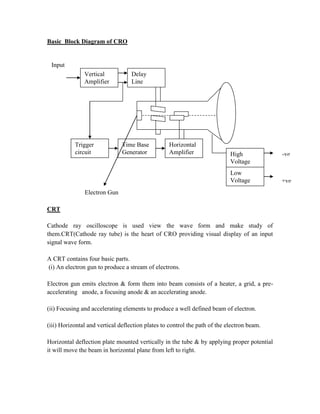
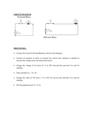
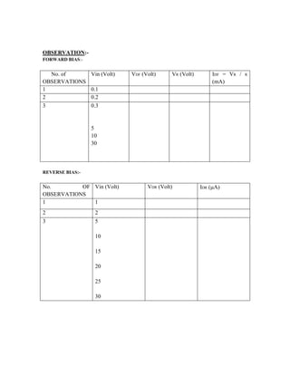
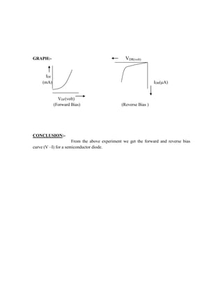
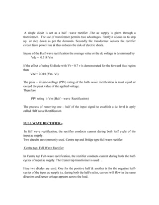
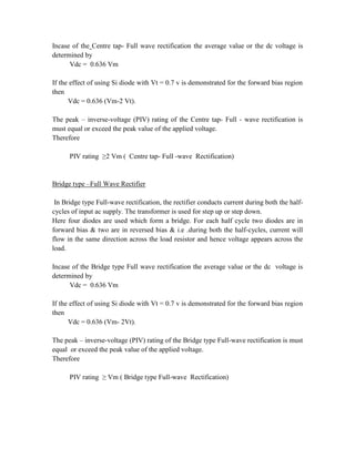
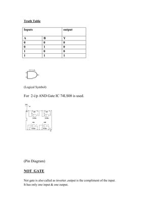
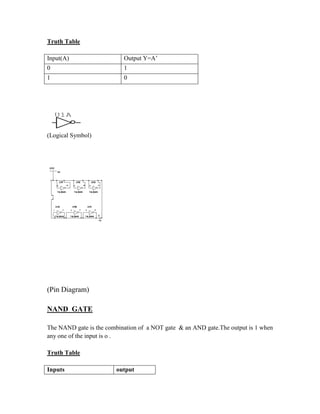
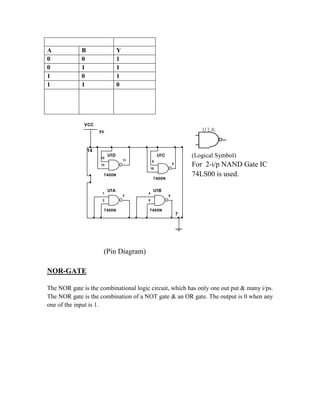
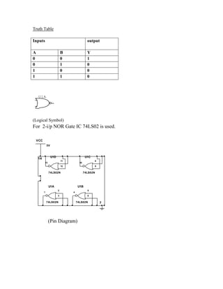
SlideShare a Scribd company logo
1 of 47
CONTENTS
SL. NO. CONTENT PAGE NO.
1. Introduction
2. General information
2.1 General discipline in the lab
2.2 Attendance
2.3 Preparation and performance
2.4 Lab reports
2.5 Precaution
3. Details of Experiment
Index
3.1 Experiment-1
Familiarity with electronics components & Devices. Testing of a
semiconductor Diode, Transistor, IC pin connection.
3.2 Experiment-2
Study of Oscilloscope to view waveforms & measure its
amplitude & Frequency.
3.3 Experiment-3
To study the VI characteristics of semiconductor Diode & to
measure its DC & AC resistance.
3.4 Experiment-4
To study the Full Wave & Half Wave Rectifier without & with
capacitor filter & to measure its r.m.s. & Average value.
3.5 Experiment-5
To plot the V- I characteristic (input and output) of an npn
transistor and measure its dc voltages and currents.
3.6 Experiment-6
Draw the gain – frequency response of BJT CE RC – coupled
amplifier.
3.7 Experiment-7
a) Study of OP-AMP in inverting and non – inverting mode.
b) OP-AMP used as integrator and differentiator.
3.8 Experiment-8
Truth table of Logic Gates.
GENERAL INSTRUCTION
INTRODUCTION:
Basic Electronics lab is a well-equipped laboratory of Electronics & Communication
Engineering Department. This lab is compulsory for B.Tech students of CSE, ECE, EE,
ME & CE. This laboratory provides an opportunity to enhance the practical knowledge
through its various experiments to be performed by the students. The list of experiments
to be performed is in accordance with BPUT, ORISSA. Most of the experiments have
engineering application and are the integral part of the engineering curriculum. This lab
manual describes the details of the experiments to be performed in the 1st
and 2nd
semester by the students.
GENERAL INFORMATION:
The purpose of conducting experiments can be stated as follows:
 To get familiarization with the basic components, devices, electronic instruments,
modules, kits etc. used for conducting instrumentation circuits.
 Circuit drawing using standard symbols as practiced in Instrumentation
Technology.
 Making proper connection in the experimental kits/modules as per the circuit
diagram and connection of appropriate power supply for energizing the circuits.
 Conducting experiments as per the guidelines and writing of results of
observation.
 Verification of theoretical results through graphs or calculations.
 Hands on experience on the experimental setup.
GENERAL DISCIPLINE IN LAB:
 Students must turn up in time and contact concerned faculty for the experiment
they are supposed to perform.
 Students will not be allowed after ten minutes from the scheduled time.
 Attendance in the laboratory is compulsory. For any absence, students have to
write an application with sufficient reasons and proof as per the BPUT rules and
regulation & may be allowed with permission of concerned HOD.
 Students will not leave the class till the period is over.
 Students should come prepared for their experiment with lab record.
 Experimental results should be entered in the lab. Record and certified /signed by
concerned faculty/lab instructor.
 Students must get the connection of experimental setup verified before switching
on the power supply.
 After the experiment is over, the experimental kits/modules. Measuring tools and
any other tools for the experiments should be returned to the lab instructor.
 Students should maintain silence while performing the experiments. If necessity
arises for discussion amongst them, they should discuss with a very low pitch
without disturbing the adjacent groups.
 Students should not unnecessarily fiddle with the instruments knob or any other
pot. In the instruments which may disturb the calibration accuracy, range or zero
etc.
 Violating the above code of conduct may attract disciplinary action.
ATTENDANCE:
 Attendance in the lab class is compulsory. As an incentive, certain percentage of
lab marks is allotted for attendance in the internal evaluation of lab. Performance.
 Each group of students must write a satisfactory report for each lab experiments
in order to pass the course.
 The concerned faculty will duly record attendance.
 Students should complete the experiments on the day allotted for the same.
 Failure to do so or any absence on that day may result in loosing marks in the
evaluation process of the lab records.
 However, on genuine ground, alternate time slot may be given to complete the
experiment.
 Students should not attend a different lab group/section other than the one
assigned at the beginning of the session.
 On account of illness or some family problems, if a student misses the lab.
Classes, he /she may be assigned a different group to make up the losses in
consultation with the concerned faculty member/lab instructor.
PREPARATION AND PERFORMANCE:
 Students should come to the lab thoroughly prepared on the experiments they are
assigned to perform on that day.
 Faculty may check their preparation and understanding of the experiments. If not
found satisfactory, students may be debarred from doing the experiments.
 Students should record the experimental results and observation in the lab.
Record.
 Students must bring the Record (fair and rough) on each practical class with
written records of the last experiments performed complete in all respect.
 Students without Record will not be allowed to do the experiments and hence
loose their attendance.
 Any instrument damaged or tools lost during experiments may attract punishment
in the form of fine or suspension from class.
LAB REPORTS:
 Each student is required to write a complete report of the experiment he/she has
performed and bring to lab class for evaluation in the next working lab.
 Report should be written very clearly and lab record should be maintained neatly.
 The lab must contain the following:
 Duly completed title page.
 Each report should include connection diagram (where applicable),
graphs, trace papers, equations, calculations, flow charts etc.
 Standard symbols should be used to draw the diagrams.
 Calculations and comparison with appropriate equations and
comments.
 Observation can be included explaining your experience in
conducting the experiments.
PRECAUTION:-
 Before giving power supply circuit is connected properly
 Any types of short circuits is avoided
 Any types of loose connection is avoided
 The frequency of the signal generator changed smoothly.
 Any type of parallax error in measurement is avoided.
Bhubaneswar College of Engineering, Bhubaneswar
Department of Electronics & Communication Engineering
Sessional: BE LAB
Branch:CSE/ECE/EE/ME/CE Sem: 1st
/2nd
EXPERIMENT NO:-1
AIM OF THE EXPERIMENT:-
Familiarity with electronics components & Devices. Testing of a semiconductor Diode,
Transistor, IC pin connection.
APPARATUS REQUERED:-
i) Multimeter
ii) Function Generator
iii) Resistor (for colour code)
iv) Capacitor
v) Pot.
vi) LED
vii) Diode
viii) Transistor (Metal & Plastic case)
ix) IC
THEORY:-
RESISTOR-
Types of Resistor-Resistor may be classified as Fixed and variable resistors Fixed type
Resistors are like wire wound resistor, carbon composition, cermet resistor, flim type,
fusible resistor, etc.
Wire Wound Resistor-
A wire made of tungsten is wound round an insulating core. The core is usually a
material like bakelite or cement. The resistance is determined by the length & cross
section of the wire. For Wire Wound Resistor the resistance values are from 1ohms to
several thousand ohms & power rating is 5W to 100W or more.
Carbon- Composition Resistor-
The resistance material in such resistor is powered carbon or graphite mixed with a
powered insulating material which acts as a binder. Carbon resistor are available with
resistance values from 1Ω to 20MΩ & power ratings 1/10,1/8,1/4,1/2,1& 2W.
Cermet Resistor-
A carbon coating is fired into a ceramic substrate to get a cermet resistor. Such resistor
has a precise resistance value & greater stability than carbon resistor.
Film type Resistor-
These are of two kind’s viz., Carbon-film type & metal –film type. The advantage of a
film type is that its resistance is more precise than that of carbon composition type.
Fusible Resistor-
A wire wound resistor can be made of such a material that when the specified power
rating is exceeded it burns & opens the circuit. Such a resistor therefore acts both as a
resistor & as a fuse.
CALCULATION OF RESISTANCE:-
Resistor colour coding
Black---- 0
Brown--- 1
Red--- 2
Orange--- 3
Yellow--- 4
Green--- 5
Blue--- 6
Violet--- 7
Grey--- 8
White--- 9
Resistor Tolerance-The actual resistance of a resistor usually differ somewhat from the
value marked on the resistor .this variation is called tolerance. It is usually given as a
percentage.
For Gold → ±5%
Silver→ ±10%
No Colour → ±20%
Value of Resistance, R=AB*10c +
D%
Where A=First significant band
B=Second significant band
C=Third significant band
D=Tolerance band
CALCULATION OF RESISTANCE :
Sl No Calculated Resistance Measured Resistance Remark
R
(Symbol)
POTENTIOMETERS-
A Potentiometer is a three terminal device. It is generally called a POT for short. The
variable resistors can be used as a POT. The ends are connected across voltage source.
CAPACITOR-
A capacitor is a device for storing electrical energy & releasing them whenever desired.
The ability of a capacitor to store energy is called capacitance.
Types of Capacitors-
Capacitor may be of fixed or variable capacitance types. Fixed Capacitors may be of
several kinds.
Mica Capacitor –
A mica capacitor consists of a number of mica sheets separated by sheets metal foil. The
plates are connected to two terminals .The whole system is enclosed in a plastic
insulating case. Mica capacitors can withstand large variations in temp. The leakage
current is very small.
Paper Capacitor-
A paper capacitor consists of two rolls of tinfoil separated by tissue paper as insulator.
Paper capacitor are used when the capacitance requirement is between 0.05μF &1μF
Ceramic Capacitor-
It a ceramic capacitor the dielectric is earth fired to a very high temperature. The size of
the ceramic capacitor is much smaller than a paper capacitor.
The ceramic capacitors are often used for temp. Compensation i.e. to increase or decrease
capacitance with rise of temp.
Electrolytic Capacitor-
In an electrolytic capacitor a pad of absorbent gauze soaked in a suitable electrolyte such
as borax is held between two aluminium electrodes. Though the electrolyte is wet the
capacitor can be mounted in any position. To form a capacitor during manufacture a dc
voltage is applied between the two aluminum electrodes.
An electrolytic capacitor of the same size as a 0.1 μF paper capacitor may have a
capacitance of 1000 μF or more. Voltage rating of the electrolytic capacitor is of the
order of 450V.
Electrolytic capacitor is used in circuits in which we have both dc & ac.
C
(Symbol of capacitor)
PN JUNCTION DIODE-
A PN Junction is formed by one p-type& one n-type semiconductor material .A PN
junction diode is also known as semiconductor diode.
The ideal diode has a property that it conducts very well in one direction & very poorly in
opposite direction. The diode act as a perfect conductor when forward biased & as a
perfect insulator when reversed biased.
D1
DIODE
(Symbol)
ZENER DIODE-
A diode which exhibits the zener effect is called a Zener diode. A pn diode breaks down
at the breakdown voltage due to the avalanche effect. Breakdown voltage can be reduced
by using zener diode & the doping is heavy even through the voltage is low, & this effect
is called Zener Effect.
D1
ZENER
(Symbol)
LIGHT EMITTING DIODES(LED)-
LEDs that emit infra-red radiation are used in burglar alarms. LEDs emitting visible light
are used in appliances which contain character displays & graphic displays.
The LED is operated in the forward biased condition. When operated in the reverse
direction it emits no light. Thus the LED act as a light switch emitting light when in the
forward bias position & being dark when in the reverse bias position.
LED1
LED1
(Symbol)
TRANSISTOR-
BJT
A transistor consists of a germanium or silicon crystal with three separate regions.
Middle one is called base, & the other two are called emitter & collector. There are two
types of transistors viz., NPN type & PNP type. There are two PN Junction in a transistor.
In a junction transistor both majority & minority carriers are involved in its operation.
Therefore junction transistor is called bipolar junction transistor (BJT).
Q1
PNP
Q2
NPN
Q2
NPN
(PNP-Transistor Symbol) (NPN-Transistor Symbol)
FET
FET is the field effect transistor, it has also three terminals gate, drain & source. FET is
said to be a unipolar device. Basically FETs are two types one is Junction field effect
transistor (JFET) & another is the Metal Oxide field effect transistor (MOSFET)
Q2
PJFET
Q1
NJFET
(N-Channel JFET) (P-Channel JFET)
Q2
PMOS
Q1
2N3796
(N-Channel DMOSFET) (P-Channel DMOSFET)
Q2
IRF9510
Q1
2N3796
(N-Channel EMOSFET) (P-Channel EMOSFET)
MULTIMETER-
Multimeter is a device which is used for multi-function, like it can measure voltage,
resistance of a resistor, it can detect the type of a transistor; it can measure the value of β
of a transistor etc.
A multimeter is basically a PMMC meter .To measure dc current the meter acts as an
ammeter with a low series resistance. A multimeter consisting of a dc milliammeter, a dc
voltmeter, an ac voltmeter , a microammeter & an ohmmeter.
IC
An IC(Integrated Circuit) is one in which circuit components such as transistors, diodes,
resistors, capacitors etc are automatically part of a small semiconductor chip. The size of
an IC is extremely small .No components of an IC are seen to project above the surface of
the chip.
Gnd
Trg
Out
Rst Ctl
Thr
Dis
Vcc
U1
555
Gnd
Trg
Out
Rst Ctl
Thr
Dis
Vcc
U1
555
CONCLUSION:-
The components are tested & defective components are identified. The resistance of
Registers is found out from colour codes & they match to the measured values.
Bhubaneswar College of Engineering, Bhubaneswar
Department of Electronics & Communication Engineering
Sessional: BE LAB
Branch:CSE/ECE/EE/ME/CE Sem: 1st
/2nd
EXPERIMENT NO:-2
AIM OF THE EXPERIMENT:
Study of CRO & to view waveforms & measure its amplitude & frequency.
APPARATUS REQUERED:
i) CRO
ii) CRO probes
iii) Function generator
THEORY:-
The Cathode Ray Oscilloscope is probably the most versatile tool for the development of
electronic circuits & system.
The CRO allows the amplitude of electrical signals, whether they are in the form of
voltage, current or power, to be displayed as a function of time.
The CRO depends on the movement of an electron beam, which is impinged on the
screen coated with a fluorescent material, to produce a visible spot.
If the electron beam is deflected on both the conventional axes, i.e. X-axis & Y-axis,a
two dimensional display is produced.
Basic Block Diagram of CRO
Electron Gun
CRT
Cathode ray oscilloscope is used view the wave form and make study of
them.CRT(Cathode ray tube) is the heart of CRO providing visual display of an input
signal wave form.
A CRT contains four basic parts.
(i) An electron gun to produce a stream of electrons.
Electron gun emits electron & form them into beam consists of a heater, a grid, a pre-
accelerating anode, a focusing anode & an accelerating anode.
(ii) Focusing and accelerating elements to produce a well defined beam of electron.
(iii) Horizontal and vertical deflection plates to control the path of the electron beam.
Horizontal deflection plate mounted vertically in the tube & by applying proper potential
it will move the beam in horizontal plane from left to right.
Vertical
Amplifier
Delay
Line
Trigger
circuit
Time Base
Generator
Horizontal
Amplifier High
Voltage
Low
Voltage
Input
-ve
+ve
Vertical deflection plate mounted horizontally in the tube .By applying proper potential
to this plate it will produce an electric field in vertical plane & hence the electron beam
can be made to move up & down vertically in the flouresant screen.
(iv) An evacuated glass envelope with a phosphorous coated screen, which glows visibly
when struck by electron beam.
Glass Envelope-It is a conical highly evacuated glass having vacuum inside & support
the various electrodes. The inner wall of CRT between neck & screen are coated with
aquadag, which is a conducting material. The coating is connected with accelerating
anode to catch the accidentally striking electrons & returns to the anode. This prevents
the wall of the tube from charging to a high –ve potential.
Vertical Amplifier
This is wide band amplifier used to amplify the signals in the vertical section..
Horizontal Amplifier
Horizontal Amplifier is used to amplify the sawtooth voltage before it is applied to
Horizontal deflection plates.
Delay Line
It is used to delay the signal for some time in vertical sections.
Time Base-
It is used to generate the sawtooth voltage required to deflect the beam in the horizontal
section.
Trigger Circuit
This is used to convert the incoming signal into trigger pulses so that the input signal and
the sweep frequency can be synchronized.
Output Wave
CALCULATION
Amplitude of Input signal = No. of vertical divisions * Volt/division = ____ V
Time period of Input signal = No of horizontal divisions * Time/ division = ____mS
Frequency of Input signal = 1/T = ____ Hz
CONCLUSION:
CRO is one of the most useful measuring & testing instrument both in industry as well as
research work. In this experiment we study the different features of CRO & get familiar
with the measurement of different parameter of a signal.
Bhubaneswar College of Engineering, Bhubaneswar
Department of Electronics & Communication Engineering
Sessional: BE LAB
Branch:CSE/ECE/EE/ME/CE Sem: 1st
/2nd
EXPERIMENT NO: -3
AIM OF THE EXPERIMENT:-
To study the VI characteristics of semiconductor Diode & to measure its DC & AC
resistance.
APPARATUS REQUERED:
i) Diode IN4007
ii) Resistance 1K ohm
iii) Bread board
iv) Multimeter
v) Jumpers
THEORY:-
i)Forward bias:-
When the p-type is connected to the positive terminal and n-type to the negative
terminal, is said to be forward biased.During this the voltage barrier is reduced.At some
forward voltage the potential barrier is eliminated and current starts flowing in the circuit.
ii)Reverse bias:-
When the p-type is connected to the negetive terminal and n-type to the positive
terminal,it is said to be reverse biased.During this the voltage barrier is increased to a
great extend and practically no current flows through the circuit.
CIRCUIT DIAGRAM
(Forward Bias)
+ Vin
0-30v
R1
1k
D1
DIODE
(Reverse Bias)
PROCEDURE;-
 Connect the circuit on the breadboard as shown in the diagram.
 Connect an ammeter in series to measure the current and voltmeter in parallel to
measure the voltage across the diode and resistor.
 Change the voltage of Vin from 0.1 V to 30V forward bias and take VDF and VR
readings.
 Then calculate IDF = VR / R.
 Change the value of Vin from 1 V to 30V for reverse bias and take VDR and IDR
readings.
 Plot the graph between VD Vs ID.
+
-
Vi
n
0-30V
D1
DIODE
Vr
R1
1k
OBSERVATION:-
FORWARD BIAS:-
REVERSE BIAS:-
No. OF
OBSERVATIONS
Vin (Volt) VDR (Volt) IDR (A)
1 1
2 2
3 5
10
15
20
25
30
No. of
OBSERVATIONS
Vin (Volt) VDF (Volt) VR (Volt) IDF = VR / R
(mA)
1 0.1
2 0.2
3 0.3
5
10
30
GRAPH:- VDR(volt)
IDF
(mA) IDR(A)
VDF(volt)
(Forward Bias) (Reverse Bias )
CONCLUSION:-
From the above experiment we get the forward and reverse bias
curve (V –I) for a semiconductor diode.
Bhubaneswar College of Engineering, Bhubaneswar
Department of Electronics & Communication Engineering
Sessional: BE LAB
Branch:CSE/ECE/EE/ME/CE Sem: 1st
/2nd
EXPERIMENT NO:-4
AIM OF THE EXPERIMENT:-
To study the Full Wave & Half Wave Rectifier without & with capacitor filter & to
measure its r.m.s. & average value.
APPARATUS REQUERED:
i) Rectifier kit
ii) CRO
iii) CRO probes
iv) Jumpers
THEORY:-
Rectifier-
The electric power available is usually an ac supply. the supply voltage varies
sinusoidally & has a freq of 50 Hz. But there are many application e.g. electronics circuit
where dc supply is needed.Rectifier is a device that converts ac to dc signal.
The following two rectifier circuits can be possible.
i)Half-Wave Rectifier
ii)Full- Wave Rectifier
Half –Wave Rectifier
In half-wave rectification ,the rectifier conducts current only during the positive half-
cycles of input ac supply .The negative half-cycles of the input ac supply are suppressed
i.e .during negative half-cycles ,no current is conducted and hence no voltage appears
across the load.
Therefore, current always flows in one direction through after every half cycle.
A single diode is act as a half –wave rectifier .The ac supply is given through a
transformer. The use of transformer permits two advantages. Firstly,it allows us to step
up or step down as per the demands. Secondly the transformer isolates the rectifier
circuit from power line & thus reduces the risk of electric shock.
Incase of the Half wave rectification the average value or the dc voltage is determined by
Vdc = 0.318 Vm
If the effect of using Si diode with Vt = 0.7 v is demonstrated for the forward bias region
then
Vdc = 0.318 (Vm- Vt).
The peak – inverse-voltage (PIV) rating of the half- wave rectification is must equal or
exceed the peak value of the applied voltage.
Therefore
PIV rating ≥ Vm (Half – wave Rectification)
The process of removing one – half of the input signal to establish a dc level is aptly
called Half wave Rectification
FULL WAVE RECTIFIER:-
In full wave rectification, the rectifier conducts current during both half cycle of the
input ac supply.
Two circuits are commonly used. Centre tap and Bridge type full wave rectifier.
Centre tap- Full Wave Rectifier
In Centre tap Full-wave rectification, the rectifier conducts current during both the half-
cycles of input ac supply. The Center tap transformer is used .
Here two diodes are used. One for the positive half & another is for the negative half-
cycles of the input ac supply i.e. during both the half-cycles, current will flow in the same
direction and hence voltage appears across the load.
Incase of the Centre tap- Full wave rectification the average value or the dc voltage is
determined by
Vdc = 0.636 Vm
If the effect of using Si diode with Vt = 0.7 v is demonstrated for the forward bias region
then
Vdc = 0.636 (Vm-2 Vt).
The peak – inverse-voltage (PIV) rating of the Centre tap- Full - wave rectification is
must equal or exceed the peak value of the applied voltage.
Therefore
PIV rating ≥2 Vm ( Centre tap- Full -wave Rectification)
Bridge type –Full Wave Rectifier
In Bridge type Full-wave rectification, the rectifier conducts current during both the half-
cycles of input ac supply. The transformer is used for step up or step down.
Here four diodes are used which form a bridge. For each half cycle two diodes are in
forward bias & two are in reversed bias & i.e .during both the half-cycles, current will
flow in the same direction across the load resistor and hence voltage appears across the
load.
Incase of the Bridge type Full wave rectification the average value or the dc voltage is
determined by
Vdc = 0.636 Vm
If the effect of using Si diode with Vt = 0.7 v is demonstrated for the forward bias region
then
Vdc = 0.636 (Vm- 2Vt).
The peak – inverse-voltage (PIV) rating of the Bridge type Full-wave rectification is must
equal or exceed the peak value of the applied voltage.
Therefore
PIV rating ≥ Vm ( Bridge type Full-wave Rectification)
CIRCUIT DIAGRAM:-
T1
AIR_CORE_XFORMER
V1
230V 50Hz 0Deg
D1
1N4007GP
R1
4.7kohm
A B
T
G
XSC1
(Half Wave Rectifier)
V1
230V 50Hz 0Deg R1
4.7kohm
D1
1N4007GP
C1
4.7uF
C2
4.7uF
T1
AIR_CORE_XFORMER
A B
T
G
XSC1
(Half wave rectifier with capacitive load)
V1
230V 50Hz 0Deg
T1
TS_PQ4_36
D1
1N4007GP
D2
1N4007GP
R1
4.7kohm
A B
T
G
XSC1
(Full wave center tapped)
V1
230V 50Hz 0Deg
1
2
4
3
D2
1B4B42
T1
AIR_CORE_XFORMER
R1
4.7kohm
A B
T
G
XSC1
(Full wave Bridge rectifier)
PROCEDURE:-
 Connect the circuit connection as per the diagram with the help of jumpers.
 Give the ac supply to the transformer.
 Take the output across the load resistor then with the combinations of resistor and
capacitor.
 Take the input and output trace by the help of CRO.
 Measure Vm value and measure its r.m.s and average value.
CALCULATION:-
HALF – WAVE
Vm = ----- V
Vrms = 0.5 Vm=Vm/2
Vav = 0.31 Vm=Vm/
FULL – WAVE
Vm = ---- V
Vrms = 0.707 Vm
Vav = 0.636 Vm
CONCLUSION:-
From the above experiment we conclude that the ac voltage is rectified by the help of
the rectifier and we get an unidirectional dc voltage by the help of the filter with the
ripple got minimized.
Bhubaneswar College of Engineering, Bhubaneswar
Department of Electronics & Communication Engineering
Sessional: BE LAB
Branch:CSE/ECE/EE/ME/CE Sem: 1st
/2nd
EXPERIMENT NO:-5
AIM OF THE EXPERIMENT:-
To plot the V- I characteristic (input and output) of a npn transistor and measure its dc
voltages and currents.
APPARATUS REQUIRED
i) SL 100 (npn) Transistor
ii) Pot 100K ohm
iii) Bread board
iv) Multimeter
v) 1 K, 10 K ohm resistances
vi) Connecting wires
THEORY:-
Input Characteristics:- It is the curve between the base current Ib and base-emitter
voltage Vbe at constant collector-emitter voltage Vce..
Output Characteristics:- It is the curve between the collector current Ic and collector-
emitter voltage Vce at constant base current Ib..
CIRCUIT DIAGRAM:-
+
-
Vs1
0-30V
+V
+12V
R2
200k 50%
Q1
NPN
R3
1k
R1
10k
PROCEDURE:-
 Connect the circuit as shown in the circuit diagram.
 For i/p characteristics
a) Keeping Vce constant, change Vbe in steps of 0.1 V.
b) Measure VB across the base resistance to get the base current (IB = Vb/10
K).
c) Plot the graph between Vbe Vs Ib at constant Vce.(at least 3 set of
readings) for input characteristics.
 For output characteristics: -
a) Make base current Ib fixed by adjusting the POT.
b) Go on varying Vce and note down the corresponding collector resistance
voltage (Vc).
c) Divide Vc by Rc (1 K) to get the corresponding Ic value.
d) Draw the graph between Vce Vs Ic at constant Ib (for 3 set of readings at
least).
OBSERVATION:-
INPUT:
Vce Vin (volt Vbe (volt) Vb (volt) Ib = Vb / 10K
(mA)
1v 0.1v
0.2v
0.3v
0.4v
0.9v
2v
3v
10v
12v
2v
3v
OUTPUT:-
IB VCE VC Ic = Vc / 1K(mA)
15 A 0.1v
0.2v
0.3v
0.4v
0.9v
2v
5v
20A -do-
30A -do-
GRAPH:-
Ib Ic
Vbe Vce
(Input Char.) (o/p char.)
CONCLUSION:-
The input characteristics resembles the V – I characteristics of a transistor as emitter –
base junction is forward biased. With increase in Vce, Ic increases and becomes almost
constant leading to active region
Bhubaneswar College of Engineering, Bhubaneswar
Department of Electronics & Communication Engineering
Sessional: BE LAB
Branch:CSE/ECE/EE/ME/CE Sem: 1st
/2nd
EXPERIMENT NO:-6
AIM OF THE EXPERIMENT:-
Draw the gain – frequency response of BJT CE RC – coupled amplifier.
APPARATUS REQUERED
i) RC coupled amplifier kit
ii) CRO
iii) CRO probes
iv) Function Generator
v) Connecting Wires
THEORY:-
This is most popular type of coupling because it is cheap & provides excellent audio
fidelity over a wide range of freq.It is usually used for voltage amplification.
A coupling capacitor Cc is used to connect the output of the first stage to the input of the
second stage and so on. The resistance R1,R2 and RE form the biasing and stabilization
network.
The emitter bypass capacitor offer low reactance path to the signal.The coupling
capacitor Cc transmit ac signal but block dc signal. This prevents dc interference between
various stages and the shifting of operating point.
At low frequency(< 50Hz) the reactance of Cc is quiet high and hence very small part of
the signal will pass from one stage to next stage.
At high frequency(> 20KHz) the reactance of Cc is quiet low and it behaves as a short
circuit. This increases the loading effect of the next stage and reduces the voltage gain. At
mid freq. (50hz-20Khz)the gain of the amplifier is constant.
CIRCUIT DIAGRAM:-
C4
10uF
+V
Vcc
12V
R9
390ohm
R8
2k
+V
V1
10V
C3
10uF
R7
39k
R6
7.5k
R5
2.2k
C2
10uF
R1
180k
R3
9k
R2
10k
R4
2k
C1
10uF
Q2
NPN
Q1
NPN
Vin
Vout
PROCEDURE:-
 Connect the circuit as shown in the circuit diagram on the kit.
 Adjust the amplitude of the sine wave to be 20mV or 30mV by the help of function
generator and feed it to the input.
 Vary the input frequency of the function generator say from 50 Hz to1 MHz range
and note down the corresponding output voltage by the help of the CRO .
 Calculate the voltage gain
 Draw gain Vs frequency graph & find out fH, fL &B.W.
OBSERVATION
Vin (mv) F (Hz) Vout(V) Voltage Gain =
Vout / Vin
20 50
60
70
100
200
300
1k
2k
10k
20k
30k
40k
1M
GRAPH:_-
Af
0.707Af
Gain(db)
fL fH
Freq
CONCLUSION:-
The gain increases in low frequency range remains constant in mid frequency and
decreases in high frequency .
Bhubaneswar College of Engineering, Bhubaneswar
Department of Electronics & Communication Engineering
Sessional: BE LAB
Branch:CSE/ECE/EE/ME/CE Sem: 1st
/2nd
EXPERIMENT NO:-7
AIM OF THE EXPERIMENT:-
a) Study of OP-AMP in inverting and
non – inverting mode.
b) OP-AMP used as integrator and differentiator.
APPARATUS REQUERED:-
1) 741 IC
2) Resistance 1K ,10 K,4.7K ohm
3) Bread board
4) Function Generator
5) Connecting Wires
6) CRO
7) Capacitor-0.01F,0.005F
THEORY
An OP-AMP is a direct-coupled high-gain amplifier usually consisting of one or more
differential amplifier & usually followed by a level translator & an o/p stage.the o/p
stage is generally a push-pull or push-pull complimentary symmetry pair.
An OP-AMP is available as a single integrated circuit package.
Diff. type of application of OP-AMP are
- Inverting amplifier
- Non – inverting amplifier
- OP-AMP as differentiator.
- OP-AMP used as integrator
INVERTING AMP.
CIRCUIT DIAGRAM:-
(Inverting amp.)
The current i through the resistance R1is i1 = V/R1
The current through the resistance Rf is i2= -Vo/Rf
Applying Kirchhoff’s Current Law at virtual ground point, i1=i2
=> V/R1= -Vo/Rf
=> Av= Vo/V= -Rf/R1
PROCEDURE:-
 Connect the components as shown in the circuit diagram.
 Connect the power supply (0.5v, 1KHz) from the function generator for Vi.
 Observe the output in CRO for Vo.
 Trace out input and output waveforms.
 Calculate the practical gain from the trace.
 Compare theoretical gain and practical gain.
+
- 1khz
Vin
0.5V,
Rf
10k
R1
1k
U1
IDEAL
Vout
OBSERVATION:-
No. of obs. Input
voltage in
volts
Voltage gain
= (Vo / Vi)
Theoretical
voltage gain
= (- Rf / R1)
1
2
3
4
NON-INVERTING AMP.
CIRCUIT DIAGRAM:-
+
-
Vs1
10V
U1
IDEAL
Rf
10k
R1
1k
Vout
(Non-inverting amp.)
If the current flowing through the OPAMP is negligible, its i/p impedance is very large.
Applying Kirchhoff’s Current Law
(Vo-Vs1) /Rf = Vs1 /R1
=>Av = Vo /Vs1 = 1+ Rf/R1
PROCEDURE:-
 Connect the components as shown in the circuit diagram.
 Connect the power supply (0.5v, 1KHz) from the function generator for Vi.
 Observe the output in CRO for Vo.
 Trace out input and output waveforms.
 Calculate the practical gain from the trace.
 Compare theoretical gain and practical gain.
NON- INVERTING AMPLIFIER
No. of obs. Input
voltage in
volts
Voltage gain
= (Vo / Vi)
Theoretical
voltage gain
=1+ (Rf/ R1)
1
2
3
4
INTEGRATOR
CIRCUIT DIAGRAM:-
0.01uF
+
- 1khz
Vin
1v
R1
1k
U1
IDEAL
Rf
10k
Vout
(Integrator)
The current flowing through the resistor R1, i = Vin /R1
The i/p impedance of the OPAMP being infinite, the current flows through the feedback
capacitor to produce the o/p, Vo
Vo = -1/C ∫ i dt = - 1/RC ∫ Vin dt
PROCEDURE:-
 Connect the components as shown in the circuit diagram.
 Give the input at pin no.2 both sine and square wave of amplitude 1v and
frequency 1KHz one by one.
 Observe the output in CRO. Trace the i/p & o/p wave forms.
DIFFERENTIATOR
CIRCUIT DIAGRAM:-
C1
1uF
+
- 1khz
Vin
1v
R1
1k
U1
IDEAL
Rf
10k
Vout
(Differentiator)
The charge on the capacitor C is
Q=C Vin
 Vin = Q/C
Differentiating both side with respect to time, we obtain
 dVin/dt =1/C (dQ/dt) = i /C
 Vo = - CR (dVin/dt)
PROCEDURE:-
 Connect the components as shown in the circuit diagram.
 Give the input at pin no.2 both sine and square wave of amplitude 1v and
frequency 1KHz one by one.
 Observe the output in CRO. Trace the i/p & o/p wave forms.
CONCLUSION:-
From the above experiment we found that the voltage gain of inverting amplifier is ------
-----. The voltage gain of non-inverting amplifier is -----------. Also we have studied how
differentiation and integration action takes place with the help of OP-AMP.
Bhubaneswar College of Engineering, Bhubaneswar
Department of Electronics & Communication Engineering
Sessional: BE LAB
Branch:CSE/ECE/EE/ME/CE Sem: 1st
/2nd
EXPERIMENT NO:-8
AIM OF THE EXPERIMENT:- Truth table of Logic Gates.
APPARATUS REQUIRED:-
a) Bread Board b) Jumpers
c) IC 74LS00 (NAND) d) IC 74LS02 (NOR)
e) IC 74LS04 ( NOT) f) IC 74LS08 ( AND)
g) IC 74LS32 (OR ) h) IC 74LS86 (EX-OR)
THEORY:-
A digital circuit with one or more i/p signals but only one o/p signal is called a logic
gate. The three basic logic gates that make up all digital circuits are
i) OR gate
ii) AND gate
iii) NOT gate
iv) NAND gate
v) NOR gate
vi) XOR gate
vii) BUFFER gate
viii) XNOR gate
NAND & NOR gates are called Universal gate because any other gate can be realized
by using this two gates.
OR GATE
The OR gate is the combinational logic circuit, which has only one out put & many i/ps.
Its o/p is equal to high or logic 1 if any one of the i/p is high or logic 1.
Truth Table
Inputs output
A B Y
0 0 0
0 1 1
1 0 1
1 1 1
U1A
Logic symbol
For 2-i/p OR Gate IC 74LS32 is used.
5V
VCC
7
14
U1A
74LS32N
1
2
3
U1B
74LS32N
4
5
6
U1C
74LS32N
9
10
8
U1D
74LS32N
12
13
11
(Pin Diagram)
AND GATE
AND Gate is for Multiplication. If both the i/ps are high or logic 1 then only the o/p is
high or logic 1 & for all other case o/p is low or logic 0.
Truth Table
Inputs output
A B Y
0 0 0
0 1 0
1 0 0
1 1 1
U1A
(Logical Symbol)
For 2-i/p AND Gate IC 74LS08 is used.
5V
VCC
7
14
U2A
74LS08J
1
2
3
U2B
74LS08J
4
5
6
U2C
74LS08J
9
10
8
U2D
74LS08J
12
13
11
(Pin Diagram)
NOT GATE
Not gate is also called as inverter ,output is the compliment of the input.
It has only one input & one output.
Truth Table
Input(A) Output Y=A’
0 1
1 0
U1A
(Logical Symbol)
5V
VCC
7
U1A
74LS04N
2
1
U1B
74LS04N
4
3
U1C
74LS04N
6
5
U1D
74LS04N
8
9
U1E
74LS04N
10
11
U1F
74LS04N
12
13
(Pin Diagram)
NAND GATE
The NAND gate is the combination of a NOT gate & an AND gate.The output is 1 when
any one of the input is o .
Truth Table
Inputs output
A B Y
0 0 1
0 1 1
1 0 1
1 1 0
U1A
(Logical Symbol)
For 2-i/p NAND Gate IC
74LS00 is used.
(Pin Diagram)
NOR-GATE
The NOR gate is the combinational logic circuit, which has only one out put & many i/ps.
The NOR gate is the combination of a NOT gate & an OR gate. The output is 0 when any
one of the input is 1.
U1A
7400N
1
2
3
U1B
7400N
4
5
6
U1C
7400N
9
10
8
U1D
7400N
12
13
11
5V
VCC
7
14
Truth Table
Inputs output
A B Y
0 0 1
0 1 0
1 0 0
1 1 0
U1A
(Logical Symbol)
For 2-i/p NOR Gate IC 74LS02 is used.
(Pin Diagram)
5V
VCC
7
14
U1A
74LS02N
2
3
1
U1B
74LS02N
5
6
4
U1C
74LS02N
8
9
10
U1D
74LS02N
11
12
13
XOR GATE
In this gate the output is logic 0, when both the input are same, otherwise the output is
logic 1.
Truth Table
Inputs output
A B Y
0 0 0
0 1 1
1 0 1
1 1 0
U1A
(Logical Symbol)
For 2-i/p XOR Gate IC 74LS86 is used.
5V
VCC
7
14
74LS86N
1
2
3
U1A
74LS86N
4
5
6
U1B
74LS86N
9
10
8
U1C
74LS86N
12
13
11
U1D
(Pin Diagram)
BUFFER GATE
Output is the same as the input.
It has only one input & one output.
Truth Table
Input(A) Output Y=A
0 0
1 1
U1A
(Logical Symbol)
XNOR GATE
In this gate the output is logic 1, when both the input are same ,otherwise the output is
logic 0.
Truth Table
Inputs output
A B Y
0 0 1
0 1 0
1 0 0
1 1 1
U1A
(Logical Symbol)
PROCEDURE:
 Take an IC, place it in the bread board after identifying its pin numbers.
 Connect the i/p pins to i/p switches of bread board & o/p pins to the o/p.LEDs
 Give i/p as there in the truth table and check the o/p.
OBSERVATION FOR THE TRUTH TABLE:-
A B Y= AB
AND
Y= (AB)'
NAND
Y = A+B
OR
Y= (A+B)'
NOR
Y=A(XORB)
0 0 0 1 0 1 0
0 1 0 1 1 0 1
1 0 0 1 1 0 1
1 1 1 0 1 0 0
A Y= A'
NOT
0 1
1 0
PIN DIAGRAM:
 Each IC Package contains four individual gates except NOT gates.
 NOT gate IC package contains six individual gates.
CONCLUSION:
The truth table of various Logic gates is verified.

More Related Content

What's hot (20)

Unijunction transistor
Unijunction transistorUnijunction transistor
Unijunction transistor
 
common base configuration
common base configurationcommon base configuration
common base configuration
 
Semiconductor Devices
Semiconductor DevicesSemiconductor Devices
Semiconductor Devices
 
BJT & ITS BIASING
BJT & ITS BIASINGBJT & ITS BIASING
BJT & ITS BIASING
 
PHYSICS OF SEMICONDUCTOR DEVICES
PHYSICS OF SEMICONDUCTOR DEVICESPHYSICS OF SEMICONDUCTOR DEVICES
PHYSICS OF SEMICONDUCTOR DEVICES
 
Led
LedLed
Led
 
Ujt uni junction transistor - basics
Ujt   uni junction transistor - basicsUjt   uni junction transistor - basics
Ujt uni junction transistor - basics
 
Sag calculation
Sag calculationSag calculation
Sag calculation
 
Electronic components ppt
Electronic components pptElectronic components ppt
Electronic components ppt
 
Light activated scr
Light activated scrLight activated scr
Light activated scr
 
OP-AMP.pptx
OP-AMP.pptxOP-AMP.pptx
OP-AMP.pptx
 
IGBT
IGBTIGBT
IGBT
 
Mosfet ppt by dhwani sametriya
Mosfet ppt by dhwani sametriyaMosfet ppt by dhwani sametriya
Mosfet ppt by dhwani sametriya
 
Transformer Designing
Transformer Designing Transformer Designing
Transformer Designing
 
Mosfet
MosfetMosfet
Mosfet
 
Slide Wire Dc potentiometer
Slide Wire Dc potentiometerSlide Wire Dc potentiometer
Slide Wire Dc potentiometer
 
AC FUNDAMENTALS.pptx
AC FUNDAMENTALS.pptxAC FUNDAMENTALS.pptx
AC FUNDAMENTALS.pptx
 
TRANSISTORS
 TRANSISTORS TRANSISTORS
TRANSISTORS
 
Power BJT
Power BJTPower BJT
Power BJT
 
Unijunction transistor (ujt)
Unijunction transistor (ujt)Unijunction transistor (ujt)
Unijunction transistor (ujt)
 

Similar to electronics lab.doc

EEE-214 Electronics Lab Manual.pdf
EEE-214 Electronics Lab Manual.pdfEEE-214 Electronics Lab Manual.pdf
EEE-214 Electronics Lab Manual.pdfmAkEiTeAsY13
 
206891661 ee2002-lab-manual-fall-2013
206891661 ee2002-lab-manual-fall-2013206891661 ee2002-lab-manual-fall-2013
206891661 ee2002-lab-manual-fall-2013homeworkping7
 
Electrical Circuit Lab
Electrical Circuit LabElectrical Circuit Lab
Electrical Circuit LabCyber4Tech
 
Report on PCB designing and fabrication by Prince Rohan
Report on PCB designing and fabrication by Prince RohanReport on PCB designing and fabrication by Prince Rohan
Report on PCB designing and fabrication by Prince RohanRohan Das
 
XII Physics Investigatory project-on-factors-affecting-internal-resistance-of...
XII Physics Investigatory project-on-factors-affecting-internal-resistance-of...XII Physics Investigatory project-on-factors-affecting-internal-resistance-of...
XII Physics Investigatory project-on-factors-affecting-internal-resistance-of...rajputanajaimaharana
 
Em ii lab manual 28.10.08 latest
Em ii lab manual 28.10.08 latestEm ii lab manual 28.10.08 latest
Em ii lab manual 28.10.08 latestraj_e2004
 
Engineering practice lab manual for electronics
Engineering practice lab manual for electronicsEngineering practice lab manual for electronics
Engineering practice lab manual for electronicsPadhu Ar
 
Lab manual for Basic electrical and electronics engineering for first year
Lab manual for Basic electrical and electronics engineering for first yearLab manual for Basic electrical and electronics engineering for first year
Lab manual for Basic electrical and electronics engineering for first yearOmkar Rane
 
189626882 ep227-digital-electronics
189626882 ep227-digital-electronics189626882 ep227-digital-electronics
189626882 ep227-digital-electronicsDimple Bansal
 
Electronics Lab Manual by Er. Swapnil V. Kaware
Electronics Lab Manual by Er. Swapnil V. KawareElectronics Lab Manual by Er. Swapnil V. Kaware
Electronics Lab Manual by Er. Swapnil V. KawareProf. Swapnil V. Kaware
 
Lab manual for_electronic_circuits_final_march_13_2011
Lab manual for_electronic_circuits_final_march_13_2011Lab manual for_electronic_circuits_final_march_13_2011
Lab manual for_electronic_circuits_final_march_13_2011Sachin Pal
 

Similar to electronics lab.doc (20)

EEE-214 Electronics Lab Manual.pdf
EEE-214 Electronics Lab Manual.pdfEEE-214 Electronics Lab Manual.pdf
EEE-214 Electronics Lab Manual.pdf
 
206891661 ee2002-lab-manual-fall-2013
206891661 ee2002-lab-manual-fall-2013206891661 ee2002-lab-manual-fall-2013
206891661 ee2002-lab-manual-fall-2013
 
Electrical Circuit Lab
Electrical Circuit LabElectrical Circuit Lab
Electrical Circuit Lab
 
Report on PCB designing and fabrication by Prince Rohan
Report on PCB designing and fabrication by Prince RohanReport on PCB designing and fabrication by Prince Rohan
Report on PCB designing and fabrication by Prince Rohan
 
XII Physics Investigatory project-on-factors-affecting-internal-resistance-of...
XII Physics Investigatory project-on-factors-affecting-internal-resistance-of...XII Physics Investigatory project-on-factors-affecting-internal-resistance-of...
XII Physics Investigatory project-on-factors-affecting-internal-resistance-of...
 
XII Physics Investigatory project-on-factors-affecting-internal-resistance-of...
XII Physics Investigatory project-on-factors-affecting-internal-resistance-of...XII Physics Investigatory project-on-factors-affecting-internal-resistance-of...
XII Physics Investigatory project-on-factors-affecting-internal-resistance-of...
 
Electrical testing
Electrical testingElectrical testing
Electrical testing
 
HVDCT LAB MANUAL.docx
HVDCT LAB MANUAL.docxHVDCT LAB MANUAL.docx
HVDCT LAB MANUAL.docx
 
Em ii lab manual 28.10.08 latest
Em ii lab manual 28.10.08 latestEm ii lab manual 28.10.08 latest
Em ii lab manual 28.10.08 latest
 
Hmt lab manual
Hmt lab manualHmt lab manual
Hmt lab manual
 
Engineering practice lab manual for electronics
Engineering practice lab manual for electronicsEngineering practice lab manual for electronics
Engineering practice lab manual for electronics
 
Sm lab manual
Sm lab manualSm lab manual
Sm lab manual
 
Lab manual for Basic electrical and electronics engineering for first year
Lab manual for Basic electrical and electronics engineering for first yearLab manual for Basic electrical and electronics engineering for first year
Lab manual for Basic electrical and electronics engineering for first year
 
189626882 ep227-digital-electronics
189626882 ep227-digital-electronics189626882 ep227-digital-electronics
189626882 ep227-digital-electronics
 
Gopi's mcs lab man
Gopi's mcs lab manGopi's mcs lab man
Gopi's mcs lab man
 
Electronics Lab Manual by Er. Swapnil V. Kaware
Electronics Lab Manual by Er. Swapnil V. KawareElectronics Lab Manual by Er. Swapnil V. Kaware
Electronics Lab Manual by Er. Swapnil V. Kaware
 
Spp exp 1.3
Spp exp 1.3Spp exp 1.3
Spp exp 1.3
 
Adc manual
Adc manualAdc manual
Adc manual
 
Manuval
ManuvalManuval
Manuval
 
Lab manual for_electronic_circuits_final_march_13_2011
Lab manual for_electronic_circuits_final_march_13_2011Lab manual for_electronic_circuits_final_march_13_2011
Lab manual for_electronic_circuits_final_march_13_2011
 

Recently uploaded

Software and Systems Engineering Standards: Verification and Validation of Sy...
Software and Systems Engineering Standards: Verification and Validation of Sy...Software and Systems Engineering Standards: Verification and Validation of Sy...
Software and Systems Engineering Standards: Verification and Validation of Sy...VICTOR MAESTRE RAMIREZ
 
Architect Hassan Khalil Portfolio for 2024
Architect Hassan Khalil Portfolio for 2024Architect Hassan Khalil Portfolio for 2024
Architect Hassan Khalil Portfolio for 2024hassan khalil
 
(MEERA) Dapodi Call Girls Just Call 7001035870 [ Cash on Delivery ] Pune Escorts
(MEERA) Dapodi Call Girls Just Call 7001035870 [ Cash on Delivery ] Pune Escorts(MEERA) Dapodi Call Girls Just Call 7001035870 [ Cash on Delivery ] Pune Escorts
(MEERA) Dapodi Call Girls Just Call 7001035870 [ Cash on Delivery ] Pune Escortsranjana rawat
 
GDSC ASEB Gen AI study jams presentation
GDSC ASEB Gen AI study jams presentationGDSC ASEB Gen AI study jams presentation
GDSC ASEB Gen AI study jams presentationGDSCAESB
 
Study on Air-Water & Water-Water Heat Exchange in a Finned Tube Exchanger
Study on Air-Water & Water-Water Heat Exchange in a Finned Tube ExchangerStudy on Air-Water & Water-Water Heat Exchange in a Finned Tube Exchanger
Study on Air-Water & Water-Water Heat Exchange in a Finned Tube ExchangerAnamika Sarkar
 
VIP Call Girls Service Hitech City Hyderabad Call +91-8250192130
VIP Call Girls Service Hitech City Hyderabad Call +91-8250192130VIP Call Girls Service Hitech City Hyderabad Call +91-8250192130
VIP Call Girls Service Hitech City Hyderabad Call +91-8250192130Suhani Kapoor
 
Call Girls Narol 7397865700 Independent Call Girls
Call Girls Narol 7397865700 Independent Call GirlsCall Girls Narol 7397865700 Independent Call Girls
Call Girls Narol 7397865700 Independent Call Girlsssuser7cb4ff
 
High Profile Call Girls Nagpur Isha Call 7001035870 Meet With Nagpur Escorts
High Profile Call Girls Nagpur Isha Call 7001035870 Meet With Nagpur EscortsHigh Profile Call Girls Nagpur Isha Call 7001035870 Meet With Nagpur Escorts
High Profile Call Girls Nagpur Isha Call 7001035870 Meet With Nagpur Escortsranjana rawat
 
High Profile Call Girls Nagpur Meera Call 7001035870 Meet With Nagpur Escorts
High Profile Call Girls Nagpur Meera Call 7001035870 Meet With Nagpur EscortsHigh Profile Call Girls Nagpur Meera Call 7001035870 Meet With Nagpur Escorts
High Profile Call Girls Nagpur Meera Call 7001035870 Meet With Nagpur EscortsCall Girls in Nagpur High Profile
 
Call Girls Delhi {Jodhpur} 9711199012 high profile service
Call Girls Delhi {Jodhpur} 9711199012 high profile serviceCall Girls Delhi {Jodhpur} 9711199012 high profile service
Call Girls Delhi {Jodhpur} 9711199012 high profile servicerehmti665
 
VICTOR MAESTRE RAMIREZ - Planetary Defender on NASA's Double Asteroid Redirec...
VICTOR MAESTRE RAMIREZ - Planetary Defender on NASA's Double Asteroid Redirec...VICTOR MAESTRE RAMIREZ - Planetary Defender on NASA's Double Asteroid Redirec...
VICTOR MAESTRE RAMIREZ - Planetary Defender on NASA's Double Asteroid Redirec...VICTOR MAESTRE RAMIREZ
 
Oxy acetylene welding presentation note.
Oxy acetylene welding presentation note.Oxy acetylene welding presentation note.
Oxy acetylene welding presentation note.eptoze12
 
Introduction to Microprocesso programming and interfacing.pptx
Introduction to Microprocesso programming and interfacing.pptxIntroduction to Microprocesso programming and interfacing.pptx
Introduction to Microprocesso programming and interfacing.pptxvipinkmenon1
 
IVE Industry Focused Event - Defence Sector 2024
IVE Industry Focused Event - Defence Sector 2024IVE Industry Focused Event - Defence Sector 2024
IVE Industry Focused Event - Defence Sector 2024Mark Billinghurst
 
Artificial-Intelligence-in-Electronics (K).pptx
Artificial-Intelligence-in-Electronics (K).pptxArtificial-Intelligence-in-Electronics (K).pptx
Artificial-Intelligence-in-Electronics (K).pptxbritheesh05
 
main PPT.pptx of girls hostel security using rfid
main PPT.pptx of girls hostel security using rfidmain PPT.pptx of girls hostel security using rfid
main PPT.pptx of girls hostel security using rfidNikhilNagaraju
 
HARMONY IN THE HUMAN BEING - Unit-II UHV-2
HARMONY IN THE HUMAN BEING - Unit-II UHV-2HARMONY IN THE HUMAN BEING - Unit-II UHV-2
HARMONY IN THE HUMAN BEING - Unit-II UHV-2RajaP95
 
APPLICATIONS-AC/DC DRIVES-OPERATING CHARACTERISTICS
APPLICATIONS-AC/DC DRIVES-OPERATING CHARACTERISTICSAPPLICATIONS-AC/DC DRIVES-OPERATING CHARACTERISTICS
APPLICATIONS-AC/DC DRIVES-OPERATING CHARACTERISTICSKurinjimalarL3
 

Recently uploaded (20)

Software and Systems Engineering Standards: Verification and Validation of Sy...
Software and Systems Engineering Standards: Verification and Validation of Sy...Software and Systems Engineering Standards: Verification and Validation of Sy...
Software and Systems Engineering Standards: Verification and Validation of Sy...
 
Architect Hassan Khalil Portfolio for 2024
Architect Hassan Khalil Portfolio for 2024Architect Hassan Khalil Portfolio for 2024
Architect Hassan Khalil Portfolio for 2024
 
(MEERA) Dapodi Call Girls Just Call 7001035870 [ Cash on Delivery ] Pune Escorts
(MEERA) Dapodi Call Girls Just Call 7001035870 [ Cash on Delivery ] Pune Escorts(MEERA) Dapodi Call Girls Just Call 7001035870 [ Cash on Delivery ] Pune Escorts
(MEERA) Dapodi Call Girls Just Call 7001035870 [ Cash on Delivery ] Pune Escorts
 
9953056974 Call Girls In South Ex, Escorts (Delhi) NCR.pdf
9953056974 Call Girls In South Ex, Escorts (Delhi) NCR.pdf9953056974 Call Girls In South Ex, Escorts (Delhi) NCR.pdf
9953056974 Call Girls In South Ex, Escorts (Delhi) NCR.pdf
 
Exploring_Network_Security_with_JA3_by_Rakesh Seal.pptx
Exploring_Network_Security_with_JA3_by_Rakesh Seal.pptxExploring_Network_Security_with_JA3_by_Rakesh Seal.pptx
Exploring_Network_Security_with_JA3_by_Rakesh Seal.pptx
 
GDSC ASEB Gen AI study jams presentation
GDSC ASEB Gen AI study jams presentationGDSC ASEB Gen AI study jams presentation
GDSC ASEB Gen AI study jams presentation
 
Study on Air-Water & Water-Water Heat Exchange in a Finned Tube Exchanger
Study on Air-Water & Water-Water Heat Exchange in a Finned Tube ExchangerStudy on Air-Water & Water-Water Heat Exchange in a Finned Tube Exchanger
Study on Air-Water & Water-Water Heat Exchange in a Finned Tube Exchanger
 
VIP Call Girls Service Hitech City Hyderabad Call +91-8250192130
VIP Call Girls Service Hitech City Hyderabad Call +91-8250192130VIP Call Girls Service Hitech City Hyderabad Call +91-8250192130
VIP Call Girls Service Hitech City Hyderabad Call +91-8250192130
 
Call Girls Narol 7397865700 Independent Call Girls
Call Girls Narol 7397865700 Independent Call GirlsCall Girls Narol 7397865700 Independent Call Girls
Call Girls Narol 7397865700 Independent Call Girls
 
High Profile Call Girls Nagpur Isha Call 7001035870 Meet With Nagpur Escorts
High Profile Call Girls Nagpur Isha Call 7001035870 Meet With Nagpur EscortsHigh Profile Call Girls Nagpur Isha Call 7001035870 Meet With Nagpur Escorts
High Profile Call Girls Nagpur Isha Call 7001035870 Meet With Nagpur Escorts
 
High Profile Call Girls Nagpur Meera Call 7001035870 Meet With Nagpur Escorts
High Profile Call Girls Nagpur Meera Call 7001035870 Meet With Nagpur EscortsHigh Profile Call Girls Nagpur Meera Call 7001035870 Meet With Nagpur Escorts
High Profile Call Girls Nagpur Meera Call 7001035870 Meet With Nagpur Escorts
 
Call Girls Delhi {Jodhpur} 9711199012 high profile service
Call Girls Delhi {Jodhpur} 9711199012 high profile serviceCall Girls Delhi {Jodhpur} 9711199012 high profile service
Call Girls Delhi {Jodhpur} 9711199012 high profile service
 
VICTOR MAESTRE RAMIREZ - Planetary Defender on NASA's Double Asteroid Redirec...
VICTOR MAESTRE RAMIREZ - Planetary Defender on NASA's Double Asteroid Redirec...VICTOR MAESTRE RAMIREZ - Planetary Defender on NASA's Double Asteroid Redirec...
VICTOR MAESTRE RAMIREZ - Planetary Defender on NASA's Double Asteroid Redirec...
 
Oxy acetylene welding presentation note.
Oxy acetylene welding presentation note.Oxy acetylene welding presentation note.
Oxy acetylene welding presentation note.
 
Introduction to Microprocesso programming and interfacing.pptx
Introduction to Microprocesso programming and interfacing.pptxIntroduction to Microprocesso programming and interfacing.pptx
Introduction to Microprocesso programming and interfacing.pptx
 
IVE Industry Focused Event - Defence Sector 2024
IVE Industry Focused Event - Defence Sector 2024IVE Industry Focused Event - Defence Sector 2024
IVE Industry Focused Event - Defence Sector 2024
 
Artificial-Intelligence-in-Electronics (K).pptx
Artificial-Intelligence-in-Electronics (K).pptxArtificial-Intelligence-in-Electronics (K).pptx
Artificial-Intelligence-in-Electronics (K).pptx
 
main PPT.pptx of girls hostel security using rfid
main PPT.pptx of girls hostel security using rfidmain PPT.pptx of girls hostel security using rfid
main PPT.pptx of girls hostel security using rfid
 
HARMONY IN THE HUMAN BEING - Unit-II UHV-2
HARMONY IN THE HUMAN BEING - Unit-II UHV-2HARMONY IN THE HUMAN BEING - Unit-II UHV-2
HARMONY IN THE HUMAN BEING - Unit-II UHV-2
 
APPLICATIONS-AC/DC DRIVES-OPERATING CHARACTERISTICS
APPLICATIONS-AC/DC DRIVES-OPERATING CHARACTERISTICSAPPLICATIONS-AC/DC DRIVES-OPERATING CHARACTERISTICS
APPLICATIONS-AC/DC DRIVES-OPERATING CHARACTERISTICS
 

electronics lab.doc

  • 1. CONTENTS SL. NO. CONTENT PAGE NO. 1. Introduction 2. General information 2.1 General discipline in the lab 2.2 Attendance 2.3 Preparation and performance 2.4 Lab reports 2.5 Precaution 3. Details of Experiment Index 3.1 Experiment-1 Familiarity with electronics components & Devices. Testing of a semiconductor Diode, Transistor, IC pin connection. 3.2 Experiment-2 Study of Oscilloscope to view waveforms & measure its amplitude & Frequency. 3.3 Experiment-3 To study the VI characteristics of semiconductor Diode & to measure its DC & AC resistance. 3.4 Experiment-4 To study the Full Wave & Half Wave Rectifier without & with capacitor filter & to measure its r.m.s. & Average value. 3.5 Experiment-5 To plot the V- I characteristic (input and output) of an npn transistor and measure its dc voltages and currents. 3.6 Experiment-6 Draw the gain – frequency response of BJT CE RC – coupled amplifier. 3.7 Experiment-7 a) Study of OP-AMP in inverting and non – inverting mode. b) OP-AMP used as integrator and differentiator. 3.8 Experiment-8 Truth table of Logic Gates.
  • 2. GENERAL INSTRUCTION INTRODUCTION: Basic Electronics lab is a well-equipped laboratory of Electronics & Communication Engineering Department. This lab is compulsory for B.Tech students of CSE, ECE, EE, ME & CE. This laboratory provides an opportunity to enhance the practical knowledge through its various experiments to be performed by the students. The list of experiments to be performed is in accordance with BPUT, ORISSA. Most of the experiments have engineering application and are the integral part of the engineering curriculum. This lab manual describes the details of the experiments to be performed in the 1st and 2nd semester by the students. GENERAL INFORMATION: The purpose of conducting experiments can be stated as follows:  To get familiarization with the basic components, devices, electronic instruments, modules, kits etc. used for conducting instrumentation circuits.  Circuit drawing using standard symbols as practiced in Instrumentation Technology.  Making proper connection in the experimental kits/modules as per the circuit diagram and connection of appropriate power supply for energizing the circuits.  Conducting experiments as per the guidelines and writing of results of observation.  Verification of theoretical results through graphs or calculations.  Hands on experience on the experimental setup. GENERAL DISCIPLINE IN LAB:  Students must turn up in time and contact concerned faculty for the experiment they are supposed to perform.  Students will not be allowed after ten minutes from the scheduled time.
  • 3.  Attendance in the laboratory is compulsory. For any absence, students have to write an application with sufficient reasons and proof as per the BPUT rules and regulation & may be allowed with permission of concerned HOD.  Students will not leave the class till the period is over.  Students should come prepared for their experiment with lab record.  Experimental results should be entered in the lab. Record and certified /signed by concerned faculty/lab instructor.  Students must get the connection of experimental setup verified before switching on the power supply.  After the experiment is over, the experimental kits/modules. Measuring tools and any other tools for the experiments should be returned to the lab instructor.  Students should maintain silence while performing the experiments. If necessity arises for discussion amongst them, they should discuss with a very low pitch without disturbing the adjacent groups.  Students should not unnecessarily fiddle with the instruments knob or any other pot. In the instruments which may disturb the calibration accuracy, range or zero etc.  Violating the above code of conduct may attract disciplinary action. ATTENDANCE:  Attendance in the lab class is compulsory. As an incentive, certain percentage of lab marks is allotted for attendance in the internal evaluation of lab. Performance.  Each group of students must write a satisfactory report for each lab experiments in order to pass the course.  The concerned faculty will duly record attendance.  Students should complete the experiments on the day allotted for the same.  Failure to do so or any absence on that day may result in loosing marks in the evaluation process of the lab records.  However, on genuine ground, alternate time slot may be given to complete the experiment.  Students should not attend a different lab group/section other than the one assigned at the beginning of the session.  On account of illness or some family problems, if a student misses the lab. Classes, he /she may be assigned a different group to make up the losses in consultation with the concerned faculty member/lab instructor.
  • 4. PREPARATION AND PERFORMANCE:  Students should come to the lab thoroughly prepared on the experiments they are assigned to perform on that day.  Faculty may check their preparation and understanding of the experiments. If not found satisfactory, students may be debarred from doing the experiments.  Students should record the experimental results and observation in the lab. Record.  Students must bring the Record (fair and rough) on each practical class with written records of the last experiments performed complete in all respect.  Students without Record will not be allowed to do the experiments and hence loose their attendance.  Any instrument damaged or tools lost during experiments may attract punishment in the form of fine or suspension from class. LAB REPORTS:  Each student is required to write a complete report of the experiment he/she has performed and bring to lab class for evaluation in the next working lab.  Report should be written very clearly and lab record should be maintained neatly.  The lab must contain the following:  Duly completed title page.  Each report should include connection diagram (where applicable), graphs, trace papers, equations, calculations, flow charts etc.  Standard symbols should be used to draw the diagrams.  Calculations and comparison with appropriate equations and comments.  Observation can be included explaining your experience in conducting the experiments. PRECAUTION:-  Before giving power supply circuit is connected properly  Any types of short circuits is avoided  Any types of loose connection is avoided  The frequency of the signal generator changed smoothly.  Any type of parallax error in measurement is avoided.
  • 5.
  • 6. Bhubaneswar College of Engineering, Bhubaneswar Department of Electronics & Communication Engineering Sessional: BE LAB Branch:CSE/ECE/EE/ME/CE Sem: 1st /2nd EXPERIMENT NO:-1 AIM OF THE EXPERIMENT:- Familiarity with electronics components & Devices. Testing of a semiconductor Diode, Transistor, IC pin connection. APPARATUS REQUERED:- i) Multimeter ii) Function Generator iii) Resistor (for colour code) iv) Capacitor v) Pot. vi) LED vii) Diode viii) Transistor (Metal & Plastic case) ix) IC THEORY:- RESISTOR- Types of Resistor-Resistor may be classified as Fixed and variable resistors Fixed type Resistors are like wire wound resistor, carbon composition, cermet resistor, flim type, fusible resistor, etc. Wire Wound Resistor- A wire made of tungsten is wound round an insulating core. The core is usually a material like bakelite or cement. The resistance is determined by the length & cross section of the wire. For Wire Wound Resistor the resistance values are from 1ohms to several thousand ohms & power rating is 5W to 100W or more. Carbon- Composition Resistor- The resistance material in such resistor is powered carbon or graphite mixed with a powered insulating material which acts as a binder. Carbon resistor are available with resistance values from 1Ω to 20MΩ & power ratings 1/10,1/8,1/4,1/2,1& 2W.
  • 7. Cermet Resistor- A carbon coating is fired into a ceramic substrate to get a cermet resistor. Such resistor has a precise resistance value & greater stability than carbon resistor. Film type Resistor- These are of two kind’s viz., Carbon-film type & metal –film type. The advantage of a film type is that its resistance is more precise than that of carbon composition type. Fusible Resistor- A wire wound resistor can be made of such a material that when the specified power rating is exceeded it burns & opens the circuit. Such a resistor therefore acts both as a resistor & as a fuse. CALCULATION OF RESISTANCE:- Resistor colour coding Black---- 0 Brown--- 1 Red--- 2 Orange--- 3 Yellow--- 4 Green--- 5 Blue--- 6 Violet--- 7 Grey--- 8 White--- 9 Resistor Tolerance-The actual resistance of a resistor usually differ somewhat from the value marked on the resistor .this variation is called tolerance. It is usually given as a percentage. For Gold → ±5% Silver→ ±10% No Colour → ±20% Value of Resistance, R=AB*10c + D% Where A=First significant band B=Second significant band C=Third significant band D=Tolerance band
  • 8. CALCULATION OF RESISTANCE : Sl No Calculated Resistance Measured Resistance Remark R (Symbol) POTENTIOMETERS- A Potentiometer is a three terminal device. It is generally called a POT for short. The variable resistors can be used as a POT. The ends are connected across voltage source. CAPACITOR- A capacitor is a device for storing electrical energy & releasing them whenever desired. The ability of a capacitor to store energy is called capacitance. Types of Capacitors- Capacitor may be of fixed or variable capacitance types. Fixed Capacitors may be of several kinds. Mica Capacitor – A mica capacitor consists of a number of mica sheets separated by sheets metal foil. The plates are connected to two terminals .The whole system is enclosed in a plastic insulating case. Mica capacitors can withstand large variations in temp. The leakage current is very small. Paper Capacitor- A paper capacitor consists of two rolls of tinfoil separated by tissue paper as insulator. Paper capacitor are used when the capacitance requirement is between 0.05μF &1μF Ceramic Capacitor- It a ceramic capacitor the dielectric is earth fired to a very high temperature. The size of the ceramic capacitor is much smaller than a paper capacitor. The ceramic capacitors are often used for temp. Compensation i.e. to increase or decrease capacitance with rise of temp. Electrolytic Capacitor- In an electrolytic capacitor a pad of absorbent gauze soaked in a suitable electrolyte such as borax is held between two aluminium electrodes. Though the electrolyte is wet the
  • 9. capacitor can be mounted in any position. To form a capacitor during manufacture a dc voltage is applied between the two aluminum electrodes. An electrolytic capacitor of the same size as a 0.1 μF paper capacitor may have a capacitance of 1000 μF or more. Voltage rating of the electrolytic capacitor is of the order of 450V. Electrolytic capacitor is used in circuits in which we have both dc & ac. C (Symbol of capacitor) PN JUNCTION DIODE- A PN Junction is formed by one p-type& one n-type semiconductor material .A PN junction diode is also known as semiconductor diode. The ideal diode has a property that it conducts very well in one direction & very poorly in opposite direction. The diode act as a perfect conductor when forward biased & as a perfect insulator when reversed biased. D1 DIODE (Symbol) ZENER DIODE- A diode which exhibits the zener effect is called a Zener diode. A pn diode breaks down at the breakdown voltage due to the avalanche effect. Breakdown voltage can be reduced by using zener diode & the doping is heavy even through the voltage is low, & this effect is called Zener Effect. D1 ZENER (Symbol) LIGHT EMITTING DIODES(LED)- LEDs that emit infra-red radiation are used in burglar alarms. LEDs emitting visible light are used in appliances which contain character displays & graphic displays.
  • 10. The LED is operated in the forward biased condition. When operated in the reverse direction it emits no light. Thus the LED act as a light switch emitting light when in the forward bias position & being dark when in the reverse bias position. LED1 LED1 (Symbol) TRANSISTOR- BJT A transistor consists of a germanium or silicon crystal with three separate regions. Middle one is called base, & the other two are called emitter & collector. There are two types of transistors viz., NPN type & PNP type. There are two PN Junction in a transistor. In a junction transistor both majority & minority carriers are involved in its operation. Therefore junction transistor is called bipolar junction transistor (BJT). Q1 PNP Q2 NPN Q2 NPN (PNP-Transistor Symbol) (NPN-Transistor Symbol) FET FET is the field effect transistor, it has also three terminals gate, drain & source. FET is said to be a unipolar device. Basically FETs are two types one is Junction field effect transistor (JFET) & another is the Metal Oxide field effect transistor (MOSFET) Q2 PJFET Q1 NJFET (N-Channel JFET) (P-Channel JFET) Q2 PMOS Q1 2N3796 (N-Channel DMOSFET) (P-Channel DMOSFET)
  • 11. Q2 IRF9510 Q1 2N3796 (N-Channel EMOSFET) (P-Channel EMOSFET) MULTIMETER- Multimeter is a device which is used for multi-function, like it can measure voltage, resistance of a resistor, it can detect the type of a transistor; it can measure the value of β of a transistor etc. A multimeter is basically a PMMC meter .To measure dc current the meter acts as an ammeter with a low series resistance. A multimeter consisting of a dc milliammeter, a dc voltmeter, an ac voltmeter , a microammeter & an ohmmeter. IC An IC(Integrated Circuit) is one in which circuit components such as transistors, diodes, resistors, capacitors etc are automatically part of a small semiconductor chip. The size of an IC is extremely small .No components of an IC are seen to project above the surface of the chip. Gnd Trg Out Rst Ctl Thr Dis Vcc U1 555 Gnd Trg Out Rst Ctl Thr Dis Vcc U1 555 CONCLUSION:- The components are tested & defective components are identified. The resistance of Registers is found out from colour codes & they match to the measured values.
  • 12. Bhubaneswar College of Engineering, Bhubaneswar Department of Electronics & Communication Engineering Sessional: BE LAB Branch:CSE/ECE/EE/ME/CE Sem: 1st /2nd EXPERIMENT NO:-2 AIM OF THE EXPERIMENT: Study of CRO & to view waveforms & measure its amplitude & frequency. APPARATUS REQUERED: i) CRO ii) CRO probes iii) Function generator THEORY:- The Cathode Ray Oscilloscope is probably the most versatile tool for the development of electronic circuits & system. The CRO allows the amplitude of electrical signals, whether they are in the form of voltage, current or power, to be displayed as a function of time. The CRO depends on the movement of an electron beam, which is impinged on the screen coated with a fluorescent material, to produce a visible spot. If the electron beam is deflected on both the conventional axes, i.e. X-axis & Y-axis,a two dimensional display is produced.
  • 13. Basic Block Diagram of CRO Electron Gun CRT Cathode ray oscilloscope is used view the wave form and make study of them.CRT(Cathode ray tube) is the heart of CRO providing visual display of an input signal wave form. A CRT contains four basic parts. (i) An electron gun to produce a stream of electrons. Electron gun emits electron & form them into beam consists of a heater, a grid, a pre- accelerating anode, a focusing anode & an accelerating anode. (ii) Focusing and accelerating elements to produce a well defined beam of electron. (iii) Horizontal and vertical deflection plates to control the path of the electron beam. Horizontal deflection plate mounted vertically in the tube & by applying proper potential it will move the beam in horizontal plane from left to right. Vertical Amplifier Delay Line Trigger circuit Time Base Generator Horizontal Amplifier High Voltage Low Voltage Input -ve +ve
  • 14. Vertical deflection plate mounted horizontally in the tube .By applying proper potential to this plate it will produce an electric field in vertical plane & hence the electron beam can be made to move up & down vertically in the flouresant screen. (iv) An evacuated glass envelope with a phosphorous coated screen, which glows visibly when struck by electron beam. Glass Envelope-It is a conical highly evacuated glass having vacuum inside & support the various electrodes. The inner wall of CRT between neck & screen are coated with aquadag, which is a conducting material. The coating is connected with accelerating anode to catch the accidentally striking electrons & returns to the anode. This prevents the wall of the tube from charging to a high –ve potential. Vertical Amplifier This is wide band amplifier used to amplify the signals in the vertical section.. Horizontal Amplifier Horizontal Amplifier is used to amplify the sawtooth voltage before it is applied to Horizontal deflection plates. Delay Line It is used to delay the signal for some time in vertical sections. Time Base- It is used to generate the sawtooth voltage required to deflect the beam in the horizontal section. Trigger Circuit This is used to convert the incoming signal into trigger pulses so that the input signal and the sweep frequency can be synchronized.
  • 15. Output Wave CALCULATION Amplitude of Input signal = No. of vertical divisions * Volt/division = ____ V Time period of Input signal = No of horizontal divisions * Time/ division = ____mS Frequency of Input signal = 1/T = ____ Hz CONCLUSION: CRO is one of the most useful measuring & testing instrument both in industry as well as research work. In this experiment we study the different features of CRO & get familiar with the measurement of different parameter of a signal.
  • 16. Bhubaneswar College of Engineering, Bhubaneswar Department of Electronics & Communication Engineering Sessional: BE LAB Branch:CSE/ECE/EE/ME/CE Sem: 1st /2nd EXPERIMENT NO: -3 AIM OF THE EXPERIMENT:- To study the VI characteristics of semiconductor Diode & to measure its DC & AC resistance. APPARATUS REQUERED: i) Diode IN4007 ii) Resistance 1K ohm iii) Bread board iv) Multimeter v) Jumpers THEORY:- i)Forward bias:- When the p-type is connected to the positive terminal and n-type to the negative terminal, is said to be forward biased.During this the voltage barrier is reduced.At some forward voltage the potential barrier is eliminated and current starts flowing in the circuit. ii)Reverse bias:- When the p-type is connected to the negetive terminal and n-type to the positive terminal,it is said to be reverse biased.During this the voltage barrier is increased to a great extend and practically no current flows through the circuit.
  • 17. CIRCUIT DIAGRAM (Forward Bias) + Vin 0-30v R1 1k D1 DIODE (Reverse Bias) PROCEDURE;-  Connect the circuit on the breadboard as shown in the diagram.  Connect an ammeter in series to measure the current and voltmeter in parallel to measure the voltage across the diode and resistor.  Change the voltage of Vin from 0.1 V to 30V forward bias and take VDF and VR readings.  Then calculate IDF = VR / R.  Change the value of Vin from 1 V to 30V for reverse bias and take VDR and IDR readings.  Plot the graph between VD Vs ID. + - Vi n 0-30V D1 DIODE Vr R1 1k
  • 18. OBSERVATION:- FORWARD BIAS:- REVERSE BIAS:- No. OF OBSERVATIONS Vin (Volt) VDR (Volt) IDR (A) 1 1 2 2 3 5 10 15 20 25 30 No. of OBSERVATIONS Vin (Volt) VDF (Volt) VR (Volt) IDF = VR / R (mA) 1 0.1 2 0.2 3 0.3 5 10 30
  • 19. GRAPH:- VDR(volt) IDF (mA) IDR(A) VDF(volt) (Forward Bias) (Reverse Bias ) CONCLUSION:- From the above experiment we get the forward and reverse bias curve (V –I) for a semiconductor diode.
  • 20. Bhubaneswar College of Engineering, Bhubaneswar Department of Electronics & Communication Engineering Sessional: BE LAB Branch:CSE/ECE/EE/ME/CE Sem: 1st /2nd EXPERIMENT NO:-4 AIM OF THE EXPERIMENT:- To study the Full Wave & Half Wave Rectifier without & with capacitor filter & to measure its r.m.s. & average value. APPARATUS REQUERED: i) Rectifier kit ii) CRO iii) CRO probes iv) Jumpers THEORY:- Rectifier- The electric power available is usually an ac supply. the supply voltage varies sinusoidally & has a freq of 50 Hz. But there are many application e.g. electronics circuit where dc supply is needed.Rectifier is a device that converts ac to dc signal. The following two rectifier circuits can be possible. i)Half-Wave Rectifier ii)Full- Wave Rectifier Half –Wave Rectifier In half-wave rectification ,the rectifier conducts current only during the positive half- cycles of input ac supply .The negative half-cycles of the input ac supply are suppressed i.e .during negative half-cycles ,no current is conducted and hence no voltage appears across the load. Therefore, current always flows in one direction through after every half cycle.
  • 21. A single diode is act as a half –wave rectifier .The ac supply is given through a transformer. The use of transformer permits two advantages. Firstly,it allows us to step up or step down as per the demands. Secondly the transformer isolates the rectifier circuit from power line & thus reduces the risk of electric shock. Incase of the Half wave rectification the average value or the dc voltage is determined by Vdc = 0.318 Vm If the effect of using Si diode with Vt = 0.7 v is demonstrated for the forward bias region then Vdc = 0.318 (Vm- Vt). The peak – inverse-voltage (PIV) rating of the half- wave rectification is must equal or exceed the peak value of the applied voltage. Therefore PIV rating ≥ Vm (Half – wave Rectification) The process of removing one – half of the input signal to establish a dc level is aptly called Half wave Rectification FULL WAVE RECTIFIER:- In full wave rectification, the rectifier conducts current during both half cycle of the input ac supply. Two circuits are commonly used. Centre tap and Bridge type full wave rectifier. Centre tap- Full Wave Rectifier In Centre tap Full-wave rectification, the rectifier conducts current during both the half- cycles of input ac supply. The Center tap transformer is used . Here two diodes are used. One for the positive half & another is for the negative half- cycles of the input ac supply i.e. during both the half-cycles, current will flow in the same direction and hence voltage appears across the load.
  • 22. Incase of the Centre tap- Full wave rectification the average value or the dc voltage is determined by Vdc = 0.636 Vm If the effect of using Si diode with Vt = 0.7 v is demonstrated for the forward bias region then Vdc = 0.636 (Vm-2 Vt). The peak – inverse-voltage (PIV) rating of the Centre tap- Full - wave rectification is must equal or exceed the peak value of the applied voltage. Therefore PIV rating ≥2 Vm ( Centre tap- Full -wave Rectification) Bridge type –Full Wave Rectifier In Bridge type Full-wave rectification, the rectifier conducts current during both the half- cycles of input ac supply. The transformer is used for step up or step down. Here four diodes are used which form a bridge. For each half cycle two diodes are in forward bias & two are in reversed bias & i.e .during both the half-cycles, current will flow in the same direction across the load resistor and hence voltage appears across the load. Incase of the Bridge type Full wave rectification the average value or the dc voltage is determined by Vdc = 0.636 Vm If the effect of using Si diode with Vt = 0.7 v is demonstrated for the forward bias region then Vdc = 0.636 (Vm- 2Vt). The peak – inverse-voltage (PIV) rating of the Bridge type Full-wave rectification is must equal or exceed the peak value of the applied voltage. Therefore PIV rating ≥ Vm ( Bridge type Full-wave Rectification)
  • 23. CIRCUIT DIAGRAM:- T1 AIR_CORE_XFORMER V1 230V 50Hz 0Deg D1 1N4007GP R1 4.7kohm A B T G XSC1 (Half Wave Rectifier) V1 230V 50Hz 0Deg R1 4.7kohm D1 1N4007GP C1 4.7uF C2 4.7uF T1 AIR_CORE_XFORMER A B T G XSC1 (Half wave rectifier with capacitive load)
  • 24. V1 230V 50Hz 0Deg T1 TS_PQ4_36 D1 1N4007GP D2 1N4007GP R1 4.7kohm A B T G XSC1 (Full wave center tapped) V1 230V 50Hz 0Deg 1 2 4 3 D2 1B4B42 T1 AIR_CORE_XFORMER R1 4.7kohm A B T G XSC1 (Full wave Bridge rectifier) PROCEDURE:-  Connect the circuit connection as per the diagram with the help of jumpers.  Give the ac supply to the transformer.  Take the output across the load resistor then with the combinations of resistor and capacitor.  Take the input and output trace by the help of CRO.  Measure Vm value and measure its r.m.s and average value.
  • 25. CALCULATION:- HALF – WAVE Vm = ----- V Vrms = 0.5 Vm=Vm/2 Vav = 0.31 Vm=Vm/ FULL – WAVE Vm = ---- V Vrms = 0.707 Vm Vav = 0.636 Vm CONCLUSION:- From the above experiment we conclude that the ac voltage is rectified by the help of the rectifier and we get an unidirectional dc voltage by the help of the filter with the ripple got minimized.
  • 26. Bhubaneswar College of Engineering, Bhubaneswar Department of Electronics & Communication Engineering Sessional: BE LAB Branch:CSE/ECE/EE/ME/CE Sem: 1st /2nd EXPERIMENT NO:-5 AIM OF THE EXPERIMENT:- To plot the V- I characteristic (input and output) of a npn transistor and measure its dc voltages and currents. APPARATUS REQUIRED i) SL 100 (npn) Transistor ii) Pot 100K ohm iii) Bread board iv) Multimeter v) 1 K, 10 K ohm resistances vi) Connecting wires THEORY:- Input Characteristics:- It is the curve between the base current Ib and base-emitter voltage Vbe at constant collector-emitter voltage Vce.. Output Characteristics:- It is the curve between the collector current Ic and collector- emitter voltage Vce at constant base current Ib..
  • 27. CIRCUIT DIAGRAM:- + - Vs1 0-30V +V +12V R2 200k 50% Q1 NPN R3 1k R1 10k PROCEDURE:-  Connect the circuit as shown in the circuit diagram.  For i/p characteristics a) Keeping Vce constant, change Vbe in steps of 0.1 V. b) Measure VB across the base resistance to get the base current (IB = Vb/10 K). c) Plot the graph between Vbe Vs Ib at constant Vce.(at least 3 set of readings) for input characteristics.  For output characteristics: - a) Make base current Ib fixed by adjusting the POT. b) Go on varying Vce and note down the corresponding collector resistance voltage (Vc). c) Divide Vc by Rc (1 K) to get the corresponding Ic value. d) Draw the graph between Vce Vs Ic at constant Ib (for 3 set of readings at least).
  • 28. OBSERVATION:- INPUT: Vce Vin (volt Vbe (volt) Vb (volt) Ib = Vb / 10K (mA) 1v 0.1v 0.2v 0.3v 0.4v 0.9v 2v 3v 10v 12v 2v 3v OUTPUT:- IB VCE VC Ic = Vc / 1K(mA) 15 A 0.1v 0.2v 0.3v 0.4v 0.9v 2v 5v 20A -do- 30A -do-
  • 29. GRAPH:- Ib Ic Vbe Vce (Input Char.) (o/p char.) CONCLUSION:- The input characteristics resembles the V – I characteristics of a transistor as emitter – base junction is forward biased. With increase in Vce, Ic increases and becomes almost constant leading to active region
  • 30. Bhubaneswar College of Engineering, Bhubaneswar Department of Electronics & Communication Engineering Sessional: BE LAB Branch:CSE/ECE/EE/ME/CE Sem: 1st /2nd EXPERIMENT NO:-6 AIM OF THE EXPERIMENT:- Draw the gain – frequency response of BJT CE RC – coupled amplifier. APPARATUS REQUERED i) RC coupled amplifier kit ii) CRO iii) CRO probes iv) Function Generator v) Connecting Wires THEORY:- This is most popular type of coupling because it is cheap & provides excellent audio fidelity over a wide range of freq.It is usually used for voltage amplification. A coupling capacitor Cc is used to connect the output of the first stage to the input of the second stage and so on. The resistance R1,R2 and RE form the biasing and stabilization network. The emitter bypass capacitor offer low reactance path to the signal.The coupling capacitor Cc transmit ac signal but block dc signal. This prevents dc interference between various stages and the shifting of operating point. At low frequency(< 50Hz) the reactance of Cc is quiet high and hence very small part of the signal will pass from one stage to next stage. At high frequency(> 20KHz) the reactance of Cc is quiet low and it behaves as a short circuit. This increases the loading effect of the next stage and reduces the voltage gain. At mid freq. (50hz-20Khz)the gain of the amplifier is constant.
  • 31. CIRCUIT DIAGRAM:- C4 10uF +V Vcc 12V R9 390ohm R8 2k +V V1 10V C3 10uF R7 39k R6 7.5k R5 2.2k C2 10uF R1 180k R3 9k R2 10k R4 2k C1 10uF Q2 NPN Q1 NPN Vin Vout PROCEDURE:-  Connect the circuit as shown in the circuit diagram on the kit.  Adjust the amplitude of the sine wave to be 20mV or 30mV by the help of function generator and feed it to the input.  Vary the input frequency of the function generator say from 50 Hz to1 MHz range and note down the corresponding output voltage by the help of the CRO .  Calculate the voltage gain  Draw gain Vs frequency graph & find out fH, fL &B.W.
  • 32. OBSERVATION Vin (mv) F (Hz) Vout(V) Voltage Gain = Vout / Vin 20 50 60 70 100 200 300 1k 2k 10k 20k 30k 40k 1M GRAPH:_- Af 0.707Af Gain(db) fL fH Freq CONCLUSION:- The gain increases in low frequency range remains constant in mid frequency and decreases in high frequency .
  • 33. Bhubaneswar College of Engineering, Bhubaneswar Department of Electronics & Communication Engineering Sessional: BE LAB Branch:CSE/ECE/EE/ME/CE Sem: 1st /2nd EXPERIMENT NO:-7 AIM OF THE EXPERIMENT:- a) Study of OP-AMP in inverting and non – inverting mode. b) OP-AMP used as integrator and differentiator. APPARATUS REQUERED:- 1) 741 IC 2) Resistance 1K ,10 K,4.7K ohm 3) Bread board 4) Function Generator 5) Connecting Wires 6) CRO 7) Capacitor-0.01F,0.005F THEORY An OP-AMP is a direct-coupled high-gain amplifier usually consisting of one or more differential amplifier & usually followed by a level translator & an o/p stage.the o/p stage is generally a push-pull or push-pull complimentary symmetry pair. An OP-AMP is available as a single integrated circuit package. Diff. type of application of OP-AMP are - Inverting amplifier - Non – inverting amplifier - OP-AMP as differentiator. - OP-AMP used as integrator
  • 34. INVERTING AMP. CIRCUIT DIAGRAM:- (Inverting amp.) The current i through the resistance R1is i1 = V/R1 The current through the resistance Rf is i2= -Vo/Rf Applying Kirchhoff’s Current Law at virtual ground point, i1=i2 => V/R1= -Vo/Rf => Av= Vo/V= -Rf/R1 PROCEDURE:-  Connect the components as shown in the circuit diagram.  Connect the power supply (0.5v, 1KHz) from the function generator for Vi.  Observe the output in CRO for Vo.  Trace out input and output waveforms.  Calculate the practical gain from the trace.  Compare theoretical gain and practical gain. + - 1khz Vin 0.5V, Rf 10k R1 1k U1 IDEAL Vout
  • 35. OBSERVATION:- No. of obs. Input voltage in volts Voltage gain = (Vo / Vi) Theoretical voltage gain = (- Rf / R1) 1 2 3 4 NON-INVERTING AMP. CIRCUIT DIAGRAM:- + - Vs1 10V U1 IDEAL Rf 10k R1 1k Vout (Non-inverting amp.) If the current flowing through the OPAMP is negligible, its i/p impedance is very large. Applying Kirchhoff’s Current Law (Vo-Vs1) /Rf = Vs1 /R1 =>Av = Vo /Vs1 = 1+ Rf/R1
  • 36. PROCEDURE:-  Connect the components as shown in the circuit diagram.  Connect the power supply (0.5v, 1KHz) from the function generator for Vi.  Observe the output in CRO for Vo.  Trace out input and output waveforms.  Calculate the practical gain from the trace.  Compare theoretical gain and practical gain. NON- INVERTING AMPLIFIER No. of obs. Input voltage in volts Voltage gain = (Vo / Vi) Theoretical voltage gain =1+ (Rf/ R1) 1 2 3 4 INTEGRATOR CIRCUIT DIAGRAM:- 0.01uF + - 1khz Vin 1v R1 1k U1 IDEAL Rf 10k Vout (Integrator) The current flowing through the resistor R1, i = Vin /R1
  • 37. The i/p impedance of the OPAMP being infinite, the current flows through the feedback capacitor to produce the o/p, Vo Vo = -1/C ∫ i dt = - 1/RC ∫ Vin dt PROCEDURE:-  Connect the components as shown in the circuit diagram.  Give the input at pin no.2 both sine and square wave of amplitude 1v and frequency 1KHz one by one.  Observe the output in CRO. Trace the i/p & o/p wave forms. DIFFERENTIATOR CIRCUIT DIAGRAM:- C1 1uF + - 1khz Vin 1v R1 1k U1 IDEAL Rf 10k Vout (Differentiator) The charge on the capacitor C is Q=C Vin
  • 38.  Vin = Q/C Differentiating both side with respect to time, we obtain  dVin/dt =1/C (dQ/dt) = i /C  Vo = - CR (dVin/dt) PROCEDURE:-  Connect the components as shown in the circuit diagram.  Give the input at pin no.2 both sine and square wave of amplitude 1v and frequency 1KHz one by one.  Observe the output in CRO. Trace the i/p & o/p wave forms. CONCLUSION:- From the above experiment we found that the voltage gain of inverting amplifier is ------ -----. The voltage gain of non-inverting amplifier is -----------. Also we have studied how differentiation and integration action takes place with the help of OP-AMP.
  • 39. Bhubaneswar College of Engineering, Bhubaneswar Department of Electronics & Communication Engineering Sessional: BE LAB Branch:CSE/ECE/EE/ME/CE Sem: 1st /2nd EXPERIMENT NO:-8 AIM OF THE EXPERIMENT:- Truth table of Logic Gates. APPARATUS REQUIRED:- a) Bread Board b) Jumpers c) IC 74LS00 (NAND) d) IC 74LS02 (NOR) e) IC 74LS04 ( NOT) f) IC 74LS08 ( AND) g) IC 74LS32 (OR ) h) IC 74LS86 (EX-OR) THEORY:- A digital circuit with one or more i/p signals but only one o/p signal is called a logic gate. The three basic logic gates that make up all digital circuits are i) OR gate ii) AND gate iii) NOT gate iv) NAND gate v) NOR gate vi) XOR gate vii) BUFFER gate viii) XNOR gate NAND & NOR gates are called Universal gate because any other gate can be realized by using this two gates. OR GATE The OR gate is the combinational logic circuit, which has only one out put & many i/ps. Its o/p is equal to high or logic 1 if any one of the i/p is high or logic 1.
  • 40. Truth Table Inputs output A B Y 0 0 0 0 1 1 1 0 1 1 1 1 U1A Logic symbol For 2-i/p OR Gate IC 74LS32 is used. 5V VCC 7 14 U1A 74LS32N 1 2 3 U1B 74LS32N 4 5 6 U1C 74LS32N 9 10 8 U1D 74LS32N 12 13 11 (Pin Diagram) AND GATE AND Gate is for Multiplication. If both the i/ps are high or logic 1 then only the o/p is high or logic 1 & for all other case o/p is low or logic 0.
  • 41. Truth Table Inputs output A B Y 0 0 0 0 1 0 1 0 0 1 1 1 U1A (Logical Symbol) For 2-i/p AND Gate IC 74LS08 is used. 5V VCC 7 14 U2A 74LS08J 1 2 3 U2B 74LS08J 4 5 6 U2C 74LS08J 9 10 8 U2D 74LS08J 12 13 11 (Pin Diagram) NOT GATE Not gate is also called as inverter ,output is the compliment of the input. It has only one input & one output.
  • 42. Truth Table Input(A) Output Y=A’ 0 1 1 0 U1A (Logical Symbol) 5V VCC 7 U1A 74LS04N 2 1 U1B 74LS04N 4 3 U1C 74LS04N 6 5 U1D 74LS04N 8 9 U1E 74LS04N 10 11 U1F 74LS04N 12 13 (Pin Diagram) NAND GATE The NAND gate is the combination of a NOT gate & an AND gate.The output is 1 when any one of the input is o . Truth Table Inputs output
  • 43. A B Y 0 0 1 0 1 1 1 0 1 1 1 0 U1A (Logical Symbol) For 2-i/p NAND Gate IC 74LS00 is used. (Pin Diagram) NOR-GATE The NOR gate is the combinational logic circuit, which has only one out put & many i/ps. The NOR gate is the combination of a NOT gate & an OR gate. The output is 0 when any one of the input is 1. U1A 7400N 1 2 3 U1B 7400N 4 5 6 U1C 7400N 9 10 8 U1D 7400N 12 13 11 5V VCC 7 14
  • 44. Truth Table Inputs output A B Y 0 0 1 0 1 0 1 0 0 1 1 0 U1A (Logical Symbol) For 2-i/p NOR Gate IC 74LS02 is used. (Pin Diagram) 5V VCC 7 14 U1A 74LS02N 2 3 1 U1B 74LS02N 5 6 4 U1C 74LS02N 8 9 10 U1D 74LS02N 11 12 13
  • 45. XOR GATE In this gate the output is logic 0, when both the input are same, otherwise the output is logic 1. Truth Table Inputs output A B Y 0 0 0 0 1 1 1 0 1 1 1 0 U1A (Logical Symbol) For 2-i/p XOR Gate IC 74LS86 is used. 5V VCC 7 14 74LS86N 1 2 3 U1A 74LS86N 4 5 6 U1B 74LS86N 9 10 8 U1C 74LS86N 12 13 11 U1D (Pin Diagram)
  • 46. BUFFER GATE Output is the same as the input. It has only one input & one output. Truth Table Input(A) Output Y=A 0 0 1 1 U1A (Logical Symbol) XNOR GATE In this gate the output is logic 1, when both the input are same ,otherwise the output is logic 0. Truth Table Inputs output A B Y 0 0 1 0 1 0 1 0 0 1 1 1 U1A (Logical Symbol)
  • 47. PROCEDURE:  Take an IC, place it in the bread board after identifying its pin numbers.  Connect the i/p pins to i/p switches of bread board & o/p pins to the o/p.LEDs  Give i/p as there in the truth table and check the o/p. OBSERVATION FOR THE TRUTH TABLE:- A B Y= AB AND Y= (AB)' NAND Y = A+B OR Y= (A+B)' NOR Y=A(XORB) 0 0 0 1 0 1 0 0 1 0 1 1 0 1 1 0 0 1 1 0 1 1 1 1 0 1 0 0 A Y= A' NOT 0 1 1 0 PIN DIAGRAM:  Each IC Package contains four individual gates except NOT gates.  NOT gate IC package contains six individual gates. CONCLUSION: The truth table of various Logic gates is verified.