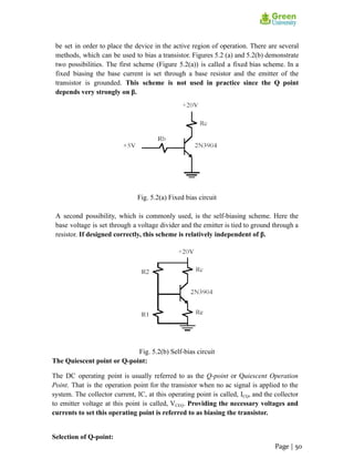
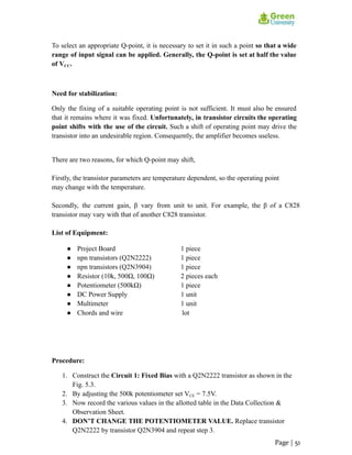
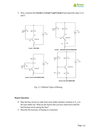
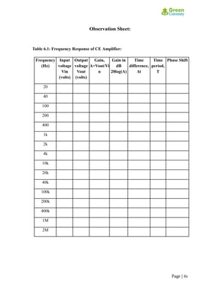
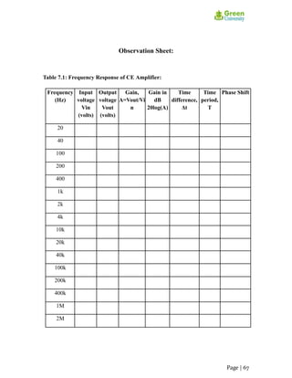
This document provides instructions and background information for an experiment to study the I-V characteristics of diodes using a circuit with a diode and resistor. Students will connect the circuit using different diode models and measure the current and voltage relationship, observing that diodes only conduct current in one direction. They will also use an AC input to observe the diode's rectifying behavior.
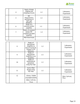
![COURSE SYLLABUS
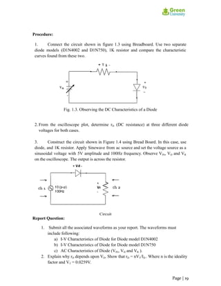
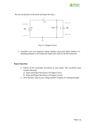
1 Faculty Faculty of Science & Engineering
2 Department Department of EEE
3 Programme BSEEE [BSc in Electrical & Electronic Engineering]
4 Name of Course Electronics Lab
5 Course Code EEE 314
6
Trimester and
Year
7 Pre-requisites Electronics I (EEE 201) and Electronics II (EEE 209)
8 Status Core EEE Course
9 Credit Hours 1.5
10 Section
11 Class Hours
12 Class Location Room: 901, Building 2
13 Course website
14
Name (s) of
Academic staff
/ Instructor(s)
15 Contact
16 Office
17 Counseling Hours
18 Text Book
1. “Microelectronics Circuits” (5th or 6th Edition) – by Adel S. Sedra &
Kenneth C. Smith. Published by Oxford University Press.
19 Reference 1. “Microelectronics Circuit Analysis and Design” (4th Edition) -
by Donald A. Neamen. Published by McGraw Hill Higher Education.
20 Equipment & Aids Electronic Hardware Equipment, Oscilloscope, Graph Paper
Page | 6](https://image.slidesharecdn.com/eee-214electronicslabmanual-230616103105-6aeb6cd5/85/EEE-214-Electronics-Lab-Manual-pdf-6-320.jpg)
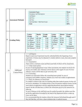
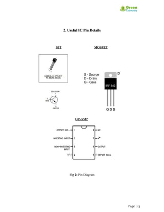


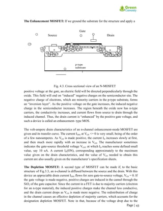
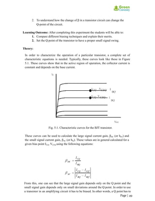
![Theory:
BJT
Transistor has two p-n junctions (see figure below). One junction is called emitter
junction and other is called collector junction. When transistor is used as an amplifier, it
is operated in active mode. In active mode, emitter junction is forward biased and
collector junction is reverse biased.
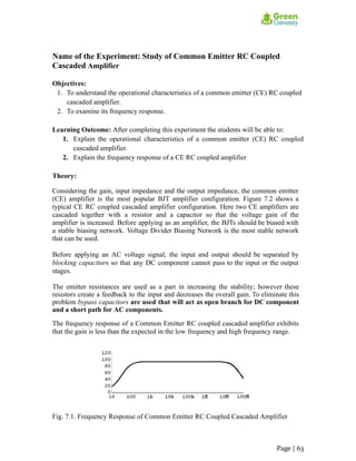
Figure 4.1
Emitter current is given by
IE = InE + IpE
We can also write
IE = IC + IB = [(1 + β)/β]IC
Where β = IC /IB is called common emitter short circuit current gain.
For a good transistor, IC>>IB i.e. β>>1. IC can also be expressed as IC = α IE. Where, α = β/
(1+β). The factor α is called common base short circuit current gain. For good
transistor, α is close to unity.
Proper dc biasing of a transistor is a prerequisite for proper operation as an amplifier.
The purpose of the biasing is to fix the IC (dc) and VCE (dc). But IC is a function of
temperature, VBE and β. It is always desirable to design a biasing circuit where IC is
insensitive to change in β.
When E-B junction is forward biased and C-B junction is reverse biased, the transistor
operates in active mode. For saturation mode of operation, both junctions are
Page | 41](https://image.slidesharecdn.com/eee-214electronicslabmanual-230616103105-6aeb6cd5/85/EEE-214-Electronics-Lab-Manual-pdf-41-320.jpg)