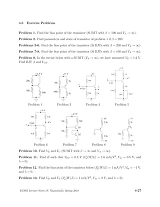
4.5 Exercise Problems
Problem 1. Find the bias point of the transistor (Si BJT with β = 100 and VA → ∞).
Problem 2. Find parameters and state of transistor of problem 1 if β = 200.
Problems 3-6. Find the bias point of the transistor (Si BJTs with β = 200 and VA → ∞).
Problems 7-8. Find the bias point of the transistor (Si BJTs with β = 100 and VA → ∞).
Problem 9. In the circuit below with a SI BJT (VA → ∞), we have measured VE = 1.2 V.
Find BJT β and VCE.
30k
20k
2.5 V
500
15 V
50k
100k
5k
3k
vo
vi
0.47 Fµ
18k
22k 1k
9 V
vi
vo
47 Fµ
µ4.7 F
270
240
15 V
34 k 1 k
5.9 k
Problem 1 Problem 3 Problem 4 Problem 5
vo
vi
16 V
1.5k
6.2k
510nF
30k
510
500
2.5 V
Q2
Q1
32k
18k
−3V
2.3k
2.3k
3V
VE
30k
5V
5V−
5k
5k
Problem 6 Problem 7 Problem 8 Problem 9
Problem 10. Find VE and VC (SI BJT with β → ∞ and VA → ∞).
Problem 11. Find R such that VDS = 0.8 V (k′
n(W/L) = 1.6 mA/V2
, Vtn = 0.5 V, and
λ = 0).
Problem 12. Find the bias point of the transistor below (k′
p(W/L) = 1 mA/V2
, Vtp = −1 V,
and λ = 0.
Problem 13. Find VD and VS (k′
n(W/L) = 1 mA/V2
, Vtn = 2 V, and λ = 0).
ECE65 Lecture Notes (F. Najmabadi), Spring 2010 4-27
4.6 Solution to Selected Exercise Problems
Problem 1. Find the bias point of the transistor (Si BJT with β = 100 and VA → ∞).
30k
20k
2.5 V
500
500
12k
1.5 V
2.5 V
This is a fixed bias scheme (because there is no RE) with a voltage divider
providing VBB (It is unstable to temperature changes, see problem 2).
Assuming BJT (PNP) in the active state and replacing R2/R1 voltage
divider with its Thevenin equivalent:
RB = 30 k 20 k = 12 k, VBB =
30
30 + 20
× 2.5 = 1.5 V
EB-KVL: 2.5 = VEB + 12 × 103
IB + 1.5
IB = (2.5 − 1.5 − 0.7)/(12 × 103
) = 25 µA
IC = βIB = 2.5 mA
EC-KVL: 2.5 = VEC + 500IC
VEC = 2.5 − 500 × 2.5 × 10−3
= 1.25 V
Since VEC ≥ 0.7 V and IC > 0, assumption of BJT in active is justified.
Bias Summary: VEC = 1.25 V, IC = 2.5 mA, and IB = 25 µA.
Problem 4. Find the bias point (Si BJT with β = 200 and VA → ∞).
vo
vi
0.47 Fµ
18k
22k 1k
9 V
VBB
RB
1k
9V
Assume BJT (NPN) in active. Replace R1/R2 voltage divider
with its Thevenin equivalent (note capacitors are open):
RB = 18 k 22 k = 9.9 k, VBB =
22
18 + 22
× 9 = 4.95 V
BE-KVL: VBB = RBIB + VBE + 103
IE IB =
IE
1 + β
=
IE
201
4.95 − 0.7 = IE
9.9 × 10³
201
+ 103
IE = 4 mA ≈ IC, IB =
IC
β
= 20 µA
CE-KVL: VCC = VCE + 103
IE
VCE = 9 − 103
× 4 × 10−3
= 5 V
Since VCE ≥ 0.7 V and IC > 0, assumption of BJT in active is justified.
Bias Summary: VCE = 5 V, IC = 4 mA, and IB = 20 µA.
ECE65 Lecture Notes (F. Najmabadi), Spring 2010 4-30
Problem 5. Find the bias point (Si BJT with β = 200 and VA → ∞).
vi
vo
47 Fµ
µ4.7 F
270
240
15 V
34 k 1 k
5.9 k
VBB
RB
270 + 240
15V
1k
= 510
Assume BJT (NPN) is in active. Replace R1/R2 voltage divider
with its Thevenin equivalent. Since capacitors are open, the
emitter resistance for bias is 270 + 240 = 510 Ω.
RB = 5.9 k 34 k = 5.0 k, VBB =
5.9
5.9 + 34
15 = 2.22 V
BE-KVL: VBB = RBIB + VBE + 510IE IB =
IE
1 + β
=
IE
201
2.22 − 0.7 = IE
5.0 × 10³
201
+ 510
IE = 3 mA ≈ IC, IB =
IC
β
= 15 µA
CE-KVL: VCC = 1000IC + VCE + 510IE
VCE = 15 − 1, 510 × 3 × 10−3
= 10.5 V
Since VCE ≥ 0.7 V and IC > 0, assumption of BJT in active is justified.
Bias Summary: VCE = 10.5 V, IC = 3 mA, and IB = 15 µA.
Problem 6. Find the bias point (Si BJT with β = 200 and VA → ∞).
vo
vi
16 V
1.5k
6.2k
510nF
30k
510
VCC VD0
6.2k
30k
−
+
−
+
VBB
RB
510
1.5k
16V
Assuming that the BJT is in the active state, the base voltage has to be large enough to
forward bias the BE junction and, therefore, the diode would also be forward biased. We
can find the Thevenin equivalent of the voltage divider part by noting (see circuit above:)
VBB = Voc =
6.2
30 + 6.2
(VCC − VD0) + VD0 = 2.74 + 0.83VD0 (V)
RB = RT = 30 k 6.2 k = 5.14 k
ECE65 Lecture Notes (F. Najmabadi), Spring 2010 4-31

Electronics 1

  • 1.
    4.5 Exercise Problems Problem1. Find the bias point of the transistor (Si BJT with β = 100 and VA → ∞). Problem 2. Find parameters and state of transistor of problem 1 if β = 200. Problems 3-6. Find the bias point of the transistor (Si BJTs with β = 200 and VA → ∞). Problems 7-8. Find the bias point of the transistor (Si BJTs with β = 100 and VA → ∞). Problem 9. In the circuit below with a SI BJT (VA → ∞), we have measured VE = 1.2 V. Find BJT β and VCE. 30k 20k 2.5 V 500 15 V 50k 100k 5k 3k vo vi 0.47 Fµ 18k 22k 1k 9 V vi vo 47 Fµ µ4.7 F 270 240 15 V 34 k 1 k 5.9 k Problem 1 Problem 3 Problem 4 Problem 5 vo vi 16 V 1.5k 6.2k 510nF 30k 510 500 2.5 V Q2 Q1 32k 18k −3V 2.3k 2.3k 3V VE 30k 5V 5V− 5k 5k Problem 6 Problem 7 Problem 8 Problem 9 Problem 10. Find VE and VC (SI BJT with β → ∞ and VA → ∞). Problem 11. Find R such that VDS = 0.8 V (k′ n(W/L) = 1.6 mA/V2 , Vtn = 0.5 V, and λ = 0). Problem 12. Find the bias point of the transistor below (k′ p(W/L) = 1 mA/V2 , Vtp = −1 V, and λ = 0. Problem 13. Find VD and VS (k′ n(W/L) = 1 mA/V2 , Vtn = 2 V, and λ = 0). ECE65 Lecture Notes (F. Najmabadi), Spring 2010 4-27
  • 2.
    4.6 Solution toSelected Exercise Problems Problem 1. Find the bias point of the transistor (Si BJT with β = 100 and VA → ∞). 30k 20k 2.5 V 500 500 12k 1.5 V 2.5 V This is a fixed bias scheme (because there is no RE) with a voltage divider providing VBB (It is unstable to temperature changes, see problem 2). Assuming BJT (PNP) in the active state and replacing R2/R1 voltage divider with its Thevenin equivalent: RB = 30 k 20 k = 12 k, VBB = 30 30 + 20 × 2.5 = 1.5 V EB-KVL: 2.5 = VEB + 12 × 103 IB + 1.5 IB = (2.5 − 1.5 − 0.7)/(12 × 103 ) = 25 µA IC = βIB = 2.5 mA EC-KVL: 2.5 = VEC + 500IC VEC = 2.5 − 500 × 2.5 × 10−3 = 1.25 V Since VEC ≥ 0.7 V and IC > 0, assumption of BJT in active is justified. Bias Summary: VEC = 1.25 V, IC = 2.5 mA, and IB = 25 µA. Problem 4. Find the bias point (Si BJT with β = 200 and VA → ∞). vo vi 0.47 Fµ 18k 22k 1k 9 V VBB RB 1k 9V Assume BJT (NPN) in active. Replace R1/R2 voltage divider with its Thevenin equivalent (note capacitors are open): RB = 18 k 22 k = 9.9 k, VBB = 22 18 + 22 × 9 = 4.95 V BE-KVL: VBB = RBIB + VBE + 103 IE IB = IE 1 + β = IE 201 4.95 − 0.7 = IE 9.9 × 10³ 201 + 103 IE = 4 mA ≈ IC, IB = IC β = 20 µA CE-KVL: VCC = VCE + 103 IE VCE = 9 − 103 × 4 × 10−3 = 5 V Since VCE ≥ 0.7 V and IC > 0, assumption of BJT in active is justified. Bias Summary: VCE = 5 V, IC = 4 mA, and IB = 20 µA. ECE65 Lecture Notes (F. Najmabadi), Spring 2010 4-30
  • 3.
    Problem 5. Findthe bias point (Si BJT with β = 200 and VA → ∞). vi vo 47 Fµ µ4.7 F 270 240 15 V 34 k 1 k 5.9 k VBB RB 270 + 240 15V 1k = 510 Assume BJT (NPN) is in active. Replace R1/R2 voltage divider with its Thevenin equivalent. Since capacitors are open, the emitter resistance for bias is 270 + 240 = 510 Ω. RB = 5.9 k 34 k = 5.0 k, VBB = 5.9 5.9 + 34 15 = 2.22 V BE-KVL: VBB = RBIB + VBE + 510IE IB = IE 1 + β = IE 201 2.22 − 0.7 = IE 5.0 × 10³ 201 + 510 IE = 3 mA ≈ IC, IB = IC β = 15 µA CE-KVL: VCC = 1000IC + VCE + 510IE VCE = 15 − 1, 510 × 3 × 10−3 = 10.5 V Since VCE ≥ 0.7 V and IC > 0, assumption of BJT in active is justified. Bias Summary: VCE = 10.5 V, IC = 3 mA, and IB = 15 µA. Problem 6. Find the bias point (Si BJT with β = 200 and VA → ∞). vo vi 16 V 1.5k 6.2k 510nF 30k 510 VCC VD0 6.2k 30k − + − + VBB RB 510 1.5k 16V Assuming that the BJT is in the active state, the base voltage has to be large enough to forward bias the BE junction and, therefore, the diode would also be forward biased. We can find the Thevenin equivalent of the voltage divider part by noting (see circuit above:) VBB = Voc = 6.2 30 + 6.2 (VCC − VD0) + VD0 = 2.74 + 0.83VD0 (V) RB = RT = 30 k 6.2 k = 5.14 k ECE65 Lecture Notes (F. Najmabadi), Spring 2010 4-31