BJT Q- POINTDESIGN
PRESENTATION
A P P L I E D E X P E R I M E N T S A N D
E L E C T R O N I C S
Presented By:
茱席拉 4090H430
孟沙克 4090H439
馬希布 4090H411
艾米略 4090H424
柯多明 4090H434
倫諾思 C100H004
奧洛林 4090H445
Date:
7th
January, 2022
2.
OVERVIE
W
• Goals
• Constraints
•Given Information
Sources of Information
• Fundamental Equations/
Laws
• Questions during design
process
• Test of Values
• Final result for BJT bias
3.
GOALS
1
• Design aquiescent point,
Q1 to be Icq=50 mA
• The goal of Transistor
Biasing is to establish a
known quiescent
operating point, or Q-
point for the bipolar
transistor to work
4.
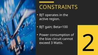
CONSTRAINTS
• BJT operatesin the
active region.
• BJT gain; Beta=100
• Power consumption of
the bias circuit cannot
exceed 3 Watts.
2
5.
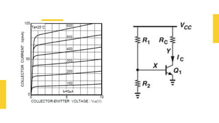
GIVEN
INFORMATION
3
•BJT output characteristicsgraph
•Bias circuit (Voltage divider Bias
Configuration) ~in our case there is no
resistor at the emitter a.k.a (Resistive Divider
Biasing without Emitter Degeneration)
•Saturation current, Is=5×10-16
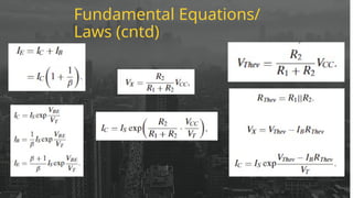
Design thought-process
(with calculations)
5
•Since BJT operates in the active region and Icq=50mA, what should the max
value of Ic be?
• With a maximum power consumption of 3W, what is the maximum supply
voltage Vcc allowed?
• Now that we have the max Vcc allowed, what value should we actually use,
considering possible fluctuations in current and voltage drops throughout
the circuit?
• With the agreed value of Vcc, and using the BJT characteristic graph, what
10.
Design thought-process
(Contd)
•What shouldthe maximum value of Rc be?
•Since saturation current value is given and Icq is known, what should be the
Vbe value of the transistor?
11.
•Taking into accountthe rule of thumb
{ I2=~Ic÷10 } for a voltage divider circuit,
where I2 is the current flowing through R2,
what is a suitable value for R2?
•What should be the value of R1 that coincides
with the calculated values of R2, Vcc?
12.
What should bethe value of R1 that coincides
with the calculated values of R2, Vcc?
Using the redrawn equivalent circuit: (Thevenin
equivalent circuit)
•How can the calculated values be verified?
Additional Suggestions forCircuit Design
“While proper choice of R1 and R2 in the circuit
makes the bias relatively insensitive to Beta, the
exponential dependence of Ic upon the resistive
divider, leads to substantial bias variations.
(Such variations were encountered in the design
process). Thus the circuit is still not practical.”
The following voltage divider biasing
configuration alleviates the problem of
sensitivity to β and VBE and is the most widely
used transistor biasing method . This occurs
because Re exhibits a linear (rather than
exponential) I-V relationship. Thus an error in
Vb due to inaccuracies in R1, R2 or Vcc is
18.
Additional Suggestions forCircuit
Design
Possible Circuit Values for this configuration*:
R1 = 23.7kΩ ,R2= 2kΩ, Rc = 90Ω, Re = 10Ω Vcc= 20V, VceQ =10V
Voltage divider network biasing makes the transistor circuit
independent of changes in beta as the biasing voltages set at the
transistors base, emitter, and collector terminals are not
dependent on external circuit values.


![Multisim_simulation_project_3_^0_4[1]-2.pptx](https://cdn.slidesharecdn.com/ss_thumbnails/multisimsimulationproject3041-2-240418183400-1d9cbd89-thumbnail.jpg?width=640&height=640&fit=bounds)


