Download to read offline

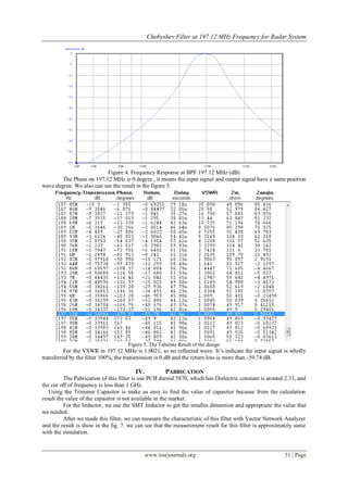
![Chebyshev Filter at 197.12 MHz Frequency for Radar System
V. Conclusion
The result of the simulation show that the calculation that we made is approximately with the real value
of the capasitor and inductor. The design from simulation we can pabricated to get the real Bandpass filter,
which has small dimention and good result for the measurement.
Acknowledgements
The author would like to thank to all my colleagues who have assistance on designed and discussed about the filter in this pa per.
REFERENCES
[1] Sayre, Cotter W. 2008. “Complete Wireless Design”. New York. Mc Graw Hill.
[2] Liu. Y, Dou W.B, and Zhao.Y. 2010. A Tri Band Bandpass Filter realized using tri-mode T shape branches. Progress in
Electromagnetic Research, Vol. 105, 425–444, 2010
[3] Christiano, Lawrence J and Fitzgerald, Terry J. “The Band Pass Filter”. NBER Working Paper
[4] White, F.J. 2004. “High Frequency Technique”. New Jersey: John Wiley & Sons, Inc.
[5] Susanti, D.N, Permana D. 2012. “Design and Simulation of 160 MHz Bandpass Filter with 60 MHz Bandwidth”.IJEN Journal Vol:12
Issue : 05 2012
www.iosrjournals.org 33 | Page](https://image.slidesharecdn.com/e0512833-130403051032-phpapp02/85/E0512833-6-320.jpg)

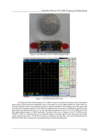
The document discusses the design and simulation of a Chebyshev bandpass filter operating at 197.12 MHz for radar systems, focusing on its applications and specifications. It outlines the calculation of required component values and provides simulation results indicating strong performance metrics including a VSWR of 1.0021 and a return loss of -59.74 dB. The results show that the simulations align closely with the expected values, leading to a successfully fabricated filter that meets radar communication needs.