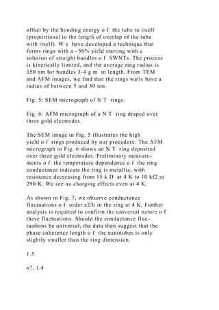
The document discusses the manipulation of individual carbon nanotubes using an atomic force microscope to create nanodevices, including field-effect transistors (FETs) and rings. It highlights the electrical properties of these nanotubes and presents techniques for producing high-yield rings of single-wall nanotubes. The results indicate significant control over the nanotubes' position and properties, enabling advanced applications in nanoelectronics.

![very high tensile strength and are extremely rigid.
Because o f these characteristics, a great number o f
applications for NTs have been proposed, such as
1D nanowires and switching elements in nano-
devices [1].
In this paper we discuss first the manipulation o f
nanotubes on a patterned substrate, then field-effect
transistors (FETs) and single-electron transistors
(SETs) in which nanotubes are the channel. Finally
we demonstrate the capability o f making rings o f
nanotubes.
2. M A N I P U L A T I O N
There is a strong Van der Waals attraction
between nanotubes, and between nanotubes and the
substrate they are deposited upon. Because o f the
high binding energy with the substrate (~0.8 eV//~
for a 1 0 0 / ~ diameter multi-wall tube [2]) the tube
can be pinned in a highly strained (bent)
configuration despite its high Young's modulus (~1
TPa). W e can manipulate the N T position at room
temperature by applying lateral forces with the tip o f
an atomic force microscope (AFM). W e found the
shear stress on surfaces such as H-passivated silicon
is high, of the order o f 10 7 N/m, such that not only
the position but also the shape o f the N T can be
controlled [2].
a ) - ~ { ~ , " b ) , , :i:: ::'
'::ii~ :~ilili!
~i ~](https://image.slidesharecdn.com/elseviermicroelectronicengineering461999101-104-221017190205-adb37b5b/85/E-L-S-E-V-I-E-R-Microelectronic-Engineering-46-1999-101-104-docx-2-320.jpg)
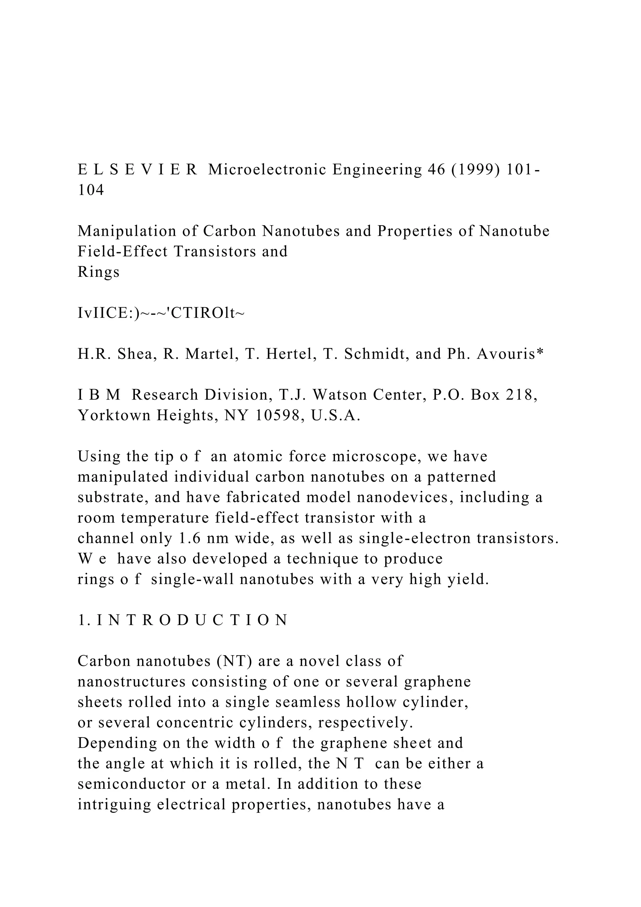
![bridging two Au electrodes deposited on a 140 nm
thick gate oxide film over a doped Si wafer, which is
used as a back gate. The source-drain current Isd
between the electrodes was measured as a function
of source-drain voltage V~d and gate-source voltage
Vg.
Nanotube
50
4O
20
10
0
- i | i i | i i I -
V ~ = ] O 0 m V 10-61 - , , , ' ' 1
i,~O~o ~" Io-~I- t 4
I0-11L , , , I J -
¢ ~ . . . ~ l b 2 ~ - 2 0 2 4 6
~ ~ vo {v)
-6 -4 -2 0 2 4 6 8
vQ (v)
Fig. 2: A field-effect transistor based on a single
nanotube.](https://image.slidesharecdn.com/elseviermicroelectronicengineering461999101-104-221017190205-adb37b5b/85/E-L-S-E-V-I-E-R-Microelectronic-Engineering-46-1999-101-104-docx-4-320.jpg)
![The top of Fig. 2 is a schematic diagram of the
nanotube FET. The lower section shows the room
temperature transfer characteristics Isd-V~ for several
values of Vsa for a 1.6 nm diameter SWNT. We
observe clear transistor action. For Vg<0 the Isd-V~d
curves (not shown) are linear, but become
increasingly non-linear for Vg>0, up to a point where
the current becomes immeasurably small for Vg>>0.
The inset in Fig. 2 shows the FET conductance vs.
Vg: it can be modulated by over 5 orders of
magnitude.
The nanotube FET behaves very much like a p-
channel MOSFET, and transport is dominated by
holes. The saturation at negative Vg is in part due to
the large (~ 1 MD) contact resistance.
A key issue is the origin of the holes: one
possibility is that the carrier concentration is inherent
to the nanotube. Another possibility is that most of
the holes are injected at the gold-NT contact because
of the difference in work function between the two
materials, as suggested by Tans et al. [3]. Our results
favor the first explanation, and we determine the 1D
hole density to be 9x106 cm l . This value
corresponds to 1 hole per 250 carbon atoms,
suggesting the tube is degenerate and/or highly
doped, perhaps as a results of its processing [4].
Devices made with MWNTs rather than SWNTs
typically exhibit no gate action. However, we have
successfully used deformed MWNTs as the channel
of a room temperature FET, although with a
conductance modulation only of order 2 [4].](https://image.slidesharecdn.com/elseviermicroelectronicengineering461999101-104-221017190205-adb37b5b/85/E-L-S-E-V-I-E-R-Microelectronic-Engineering-46-1999-101-104-docx-5-320.jpg)
![4. S I N G L E - E L E C T R O N T R A N S I S T O R
Because of their very small size, and the high
contact resistance, our FET devices exhibit Coulomb
blockade behavior at low temperatures, when the
charging energy e2/2C to add an electron to the tube
is much larger than kBT, where C is the capacitance
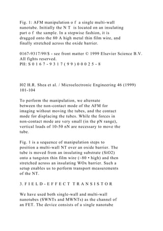
of the tube, and T temperature [5]. Fig. 3 is a plot of
Isa vs. Vg of a bundle of SWNT draped over two gold
electrodes 0.4 gm apart at 290 K, 77 K, and 4 K for
Vsa = 20 mV, 50 mV, and 5 mV, respectively. The
insets are Isd-Vsa curves at selected gate voltages.
The 290 K data show FET behavior and linear I-
V curves, with a minimum device resistance of 250
kD. At 4 K, the I-V curves have a pronounced
Coulomb gap, and there is very sharp nonmonotonic
structure in I~d vs. Vg corresponding to the lining up
of states in the tube with the Fermi level of one of
H.R. Shea et al. I Microelectronic Engineering 46 (1999) 101-
104 103
8 0 ' . ~ ;.'3 ~ ' ' ~¢'~'~'¢6~ 5 ~ , 4 , , ~ < . iTemperature =
290K Jl
8°I-~'°°E :: / ' l ~ - , i
4 0 o 4 0 ~ , . . j
0 o L I V s d ( I m V ) , I I " I I ~
-10 -5 0 5 10
Gate Voltage (V)](https://image.slidesharecdn.com/elseviermicroelectronicengineering461999101-104-221017190205-adb37b5b/85/E-L-S-E-V-I-E-R-Microelectronic-Engineering-46-1999-101-104-docx-6-320.jpg)
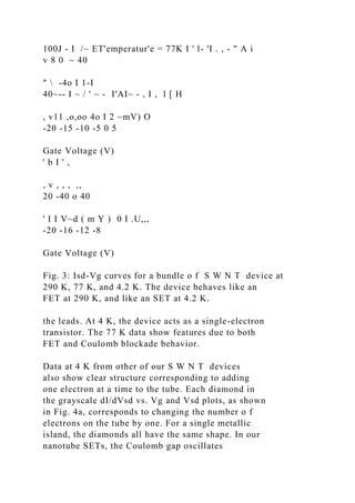
![aperiodically with Vg, which is suggestive of single-
electron transport through multiple Coulomb islands
formed within the N T bundle.
The depletion o f carriers in the tube, and the
associated decrease in tube capacitance, are clearly
visible in Fig. 4b as an increase in the width o f the
blockade region at large positive gate voltage.
It has been observed by several groups that only
a small section o f some nanotubes act as a Coulomb
island [6]. One can determine the charging energy o f
a length o f N T by calculating its capacitance.
Alternatively, one can infer the length o f the part o f
the tube that is charging from the measured charging
energy. We always observe that the length o f N T that
is charging as determined from the measured
charging energy is less than the spacing between the
electrodes by a factor o f between 1.5 and 20. This
behavior is probably attributable to multiple islands
formed within a N T bundle, and possibly also to
barriers formed along the tube due to bending o f the
tube [6,7].
a)
>~
b)
3 -
2 -
1](https://image.slidesharecdn.com/elseviermicroelectronicengineering461999101-104-221017190205-adb37b5b/85/E-L-S-E-V-I-E-R-Microelectronic-Engineering-46-1999-101-104-docx-8-320.jpg)
![" o
c 1.3
o
o
1.2
. . . . ! . . . . i . . . . i . . . .
. . , a i . . . . i . . . . I . • • •
-15 -10 -5 0 5
vg (v)
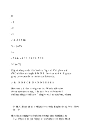
Fig. 7: Ring conductance in units of e2]h vs. Vg at 4
K for Vsd = 1 and 5 mV, showing conductance
fluctuations o f a probably universal character.
We thank A.G. Rinzler, R.E. Smalley, and H. Dai for
providing us with the single- and multi-wall
nanotubes.
REFERENCES
* e-mail address: [email protected]
1. M.S. Dresselhaus, G. Dresselhaus, and P.C.
Eklund, Science o f Fullerenes and Carbon
Nanotubes, Academic Press, San Diego, 1996
2. T. Hertel, R. Martel, and Ph. Avouris, J. Phys.
Chem. B 102 (1998) 910
3. S. J. Tans, A.R.M. Verschueren, and C. Dekker,
Nature 393 (1998) 49](https://image.slidesharecdn.com/elseviermicroelectronicengineering461999101-104-221017190205-adb37b5b/85/E-L-S-E-V-I-E-R-Microelectronic-Engineering-46-1999-101-104-docx-11-320.jpg)