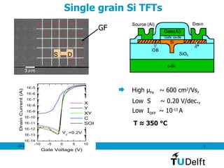
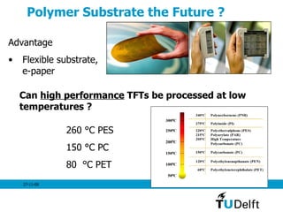
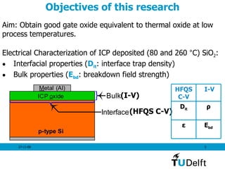
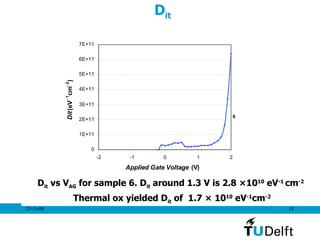
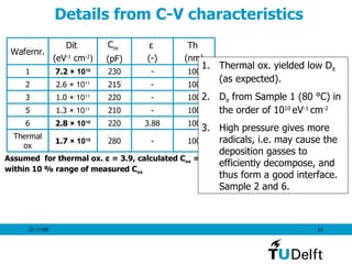
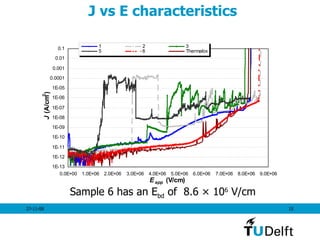
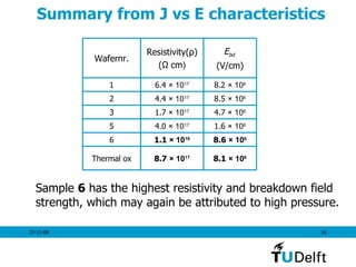
Electrical Characterization of  ICP deposited SiO 2 Oxide integrity and Interface investigation Parvesh BEng project
 Contents Introduction    Single Grain Si TFTs  Inductive Coupled Plasma A brief theory      (non) Ideal C-V   Experimental details  Various deposition conditions  Results and Discussion  C-V and J-E characteristics Conclusions
   High  µ Fe   ~ 600 cm 2 /Vs,  Low  S  ~ 0.20 V/dec.,  Low  I OFF  ~ 10 -13  A  Single grain Si TFTs T ≈ 350  °C   GF D S
Polymer Substrate the Future ? Advantage Flexible substrate,  e-paper Can  high performance  TFTs be processed at low temperatures ? 260  °C  PES 150  °C  PC 80  °C  PET
Objectives of this research (HFQS C-V) (I-V) Electrical Characterization of ICP deposited (80 and 260  ° C) SiO 2 : Interfacial properties ( D it : interface trap density) Bulk properties ( E bd : breakdown field strength) Aim: Obtain good gate oxide equivalent to thermal oxide at low process temperatures. E bd ε ρ D it I-V HFQS C-V
Solution: ICP (Inductive Coupled Plasma) TFT group of TUD proposed ICPECVD because of the following advantages over low temperature PECVD and LPCVD: Remote plasma-system High density of radicals over a wide  temperature/pressure range Independent control of the radical fluxes and the bombarding energy
Ideal Capacitance-Voltage Theory Three operation modes in C-V characteristics: Accumulation of holes at the Si/SiO 2  interface (at negative applied gate voltage). Depletion, when the holes are depleted leaving behind the acceptor ions (small positive voltage). Inversion, when the Si surface is inverted creating an electron layer at the Si/SiO 2  interface,  source   : through thermal generation of electron/hole pairs in the depletion region . C-V Characteristic
The (non) ideal frequency dependence C-V  In the ideal case: differences between  high  frequency  dQ/dV  and very  low  frequency  dQ/dV  arise in inversion mode. ( C= dQ/dV (differential charge on the gate or Si surface/differential change in voltage across the MOS capacitor) ). In the non-ideal case with dangling and strained bonds at the Si/SiO 2  interface: differences also arise in depletion mode, because these traps capture and release charges at very low frequency ac or low ramp rate.
The result and equivalent circuits High Frequency and Quasi Static C-V  characteristics D it  = C it /q A Equivalent circuits
Experimental details Reference = Thermal oxide 100 149 4 260 6 100 132 2.2 260 5 100 122 2.2 80 3 100 132 2.2 260 2 100 122 2.2 80 1 Th (nm) t  (s) p  (Pa) T  ( °C ) Wafernr. Various deposition conditions MOS capacitors on p-type,  0.1-0.2 ohm cm, (100) silicon wafers, Al contact. (Al) Ohmic contacts at backside of wafers Deposition have been performed at 80 and 260  ° C Rf power = 500 W; Gas flow Ar. = 140 sccm, SiH 4 /He (5%): 150 sccm and O 2  = 9.2 sccm. Sample 5 was exposed to oxygen plasma before deposition.
Experimental details The C-V were carried out with LCR meter (1 MHz) and 4156 C parameter analyzer (6.7 mV/s), respectively  I-V (in accumulation, sweep) measurements. The ideal process condition will be evaluated by interface trap density, resistivity at an electric field of 1 MV/cm, and the breakdown field strength (E bd ) at which the current density J exceeds 1  μ A/cm 2 .
C-V Results Process conditions: T = 260 °C, p = 4 Pa
D it D it  vs V AG  for sample 6. D it  around 1.3 V is 2.8  ×10 10  eV -1  cm -2 Thermal ox yielded D it  of  1.7 × 10 10  eV -1 cm -2
Details from C-V characteristics Assumed  for thermal ox.  ε  = 3.9, calculated C ox  = 258 pF, within 10 % range of measured C ox Thermal ox. yielded low D it  (as expected). D it  from Sample 1 (80  ° C)  in the order of 10 10  eV -1  cm -2 High pressure gives more radicals, i.e.  may cause the deposition gasses to efficiently decompose, and thus form a good interface. Sample 2 and 6. 100 3.88 220 2.8  × 10 10 6 100 - 280 1.7  × 10 10 Thermal ox 100 - 210 1.3  × 10 11 5 100 - 220 1.0  × 10 11 3 100 - 215 2.6  × 10 11 2 100 - 230 7.2  × 10 10 1 Th  (nm) ε   (-) C ox   (pF) Dit  (eV -1  cm -2 ) Wafernr.
J vs E characteristics Sample 6 has an E bd  of  8.6  × 10 6  V/cm
Summary from J vs E characteristics Sample  6  has the highest resistivity and breakdown field strength, which may again be attributed to high pressure. 8.6  × 10 6 1.1  × 10 18 6 8.1  × 10 6 8.7  × 10 17 Thermal ox 1.6  × 10 6 4.0  × 10 17 5 4.7  × 10 6 1.7  × 10 17 3 8.5  × 10 6 4.4  × 10 17 2 8.2  × 10 6 6.4  × 10 17 1 E bd   (V/cm) Resistivity( ρ ) (Ω cm ) Wafernr.
Conclusions  ICPECVD has advantages such as remote plasma-system, high density of radicals over a wide  temperature/pressure range and independent control of the radical fluxes and the bombarding energy. Deposition at T = 260  ° C yielded an Dit of 2.79  ×  10 10  eV -1  cm -2 , equivalent with that of thermal ox. 1.66  ×  10 10  eV -1  cm -2 .  Even at T = 80  ° C, Dit of 7.22  × 10 10  eV -1  cm -2  was successfully obtained.  Resistivity of 1.1  ×  10 18  Ω cm and breakdown field strength of 8.6  ×  10 6  V/cm  are comparable to thermal oxide with  ρ  of 8.7  ×  10 17  Ω cm and E bd  of 8.1 10 6  V/cm.  The experimental results show that achieving good bulk oxide and Si/SiO 2  interfacial properties with ICPECVD is promising (for future implementation in high performance (SG) TFTs) .

Presentation B Engproject

  • 1.
    Electrical Characterization of ICP deposited SiO 2 Oxide integrity and Interface investigation Parvesh BEng project
  • 2.
     Contents Introduction Single Grain Si TFTs Inductive Coupled Plasma A brief theory (non) Ideal C-V Experimental details Various deposition conditions Results and Discussion C-V and J-E characteristics Conclusions
  • 3.
    High µ Fe ~ 600 cm 2 /Vs, Low S ~ 0.20 V/dec., Low I OFF ~ 10 -13 A Single grain Si TFTs T ≈ 350 °C GF D S
  • 4.
    Polymer Substrate theFuture ? Advantage Flexible substrate, e-paper Can high performance TFTs be processed at low temperatures ? 260 °C PES 150 °C PC 80 °C PET
  • 5.
    Objectives of thisresearch (HFQS C-V) (I-V) Electrical Characterization of ICP deposited (80 and 260 ° C) SiO 2 : Interfacial properties ( D it : interface trap density) Bulk properties ( E bd : breakdown field strength) Aim: Obtain good gate oxide equivalent to thermal oxide at low process temperatures. E bd ε ρ D it I-V HFQS C-V
  • 6.
    Solution: ICP (InductiveCoupled Plasma) TFT group of TUD proposed ICPECVD because of the following advantages over low temperature PECVD and LPCVD: Remote plasma-system High density of radicals over a wide temperature/pressure range Independent control of the radical fluxes and the bombarding energy
  • 7.
    Ideal Capacitance-Voltage TheoryThree operation modes in C-V characteristics: Accumulation of holes at the Si/SiO 2 interface (at negative applied gate voltage). Depletion, when the holes are depleted leaving behind the acceptor ions (small positive voltage). Inversion, when the Si surface is inverted creating an electron layer at the Si/SiO 2 interface, source : through thermal generation of electron/hole pairs in the depletion region . C-V Characteristic
  • 8.
    The (non) idealfrequency dependence C-V In the ideal case: differences between high frequency dQ/dV and very low frequency dQ/dV arise in inversion mode. ( C= dQ/dV (differential charge on the gate or Si surface/differential change in voltage across the MOS capacitor) ). In the non-ideal case with dangling and strained bonds at the Si/SiO 2 interface: differences also arise in depletion mode, because these traps capture and release charges at very low frequency ac or low ramp rate.
  • 9.
    The result andequivalent circuits High Frequency and Quasi Static C-V characteristics D it = C it /q A Equivalent circuits
  • 10.
    Experimental details Reference= Thermal oxide 100 149 4 260 6 100 132 2.2 260 5 100 122 2.2 80 3 100 132 2.2 260 2 100 122 2.2 80 1 Th (nm) t (s) p (Pa) T ( °C ) Wafernr. Various deposition conditions MOS capacitors on p-type, 0.1-0.2 ohm cm, (100) silicon wafers, Al contact. (Al) Ohmic contacts at backside of wafers Deposition have been performed at 80 and 260 ° C Rf power = 500 W; Gas flow Ar. = 140 sccm, SiH 4 /He (5%): 150 sccm and O 2 = 9.2 sccm. Sample 5 was exposed to oxygen plasma before deposition.
  • 11.
    Experimental details TheC-V were carried out with LCR meter (1 MHz) and 4156 C parameter analyzer (6.7 mV/s), respectively I-V (in accumulation, sweep) measurements. The ideal process condition will be evaluated by interface trap density, resistivity at an electric field of 1 MV/cm, and the breakdown field strength (E bd ) at which the current density J exceeds 1 μ A/cm 2 .
  • 12.
    C-V Results Processconditions: T = 260 °C, p = 4 Pa
  • 13.
    D it Dit vs V AG for sample 6. D it around 1.3 V is 2.8 ×10 10 eV -1 cm -2 Thermal ox yielded D it of 1.7 × 10 10 eV -1 cm -2
  • 14.
    Details from C-Vcharacteristics Assumed for thermal ox. ε = 3.9, calculated C ox = 258 pF, within 10 % range of measured C ox Thermal ox. yielded low D it (as expected). D it from Sample 1 (80 ° C) in the order of 10 10 eV -1 cm -2 High pressure gives more radicals, i.e. may cause the deposition gasses to efficiently decompose, and thus form a good interface. Sample 2 and 6. 100 3.88 220 2.8 × 10 10 6 100 - 280 1.7 × 10 10 Thermal ox 100 - 210 1.3 × 10 11 5 100 - 220 1.0 × 10 11 3 100 - 215 2.6 × 10 11 2 100 - 230 7.2 × 10 10 1 Th (nm) ε (-) C ox (pF) Dit (eV -1 cm -2 ) Wafernr.
  • 15.
    J vs Echaracteristics Sample 6 has an E bd of 8.6 × 10 6 V/cm
  • 16.
    Summary from Jvs E characteristics Sample 6 has the highest resistivity and breakdown field strength, which may again be attributed to high pressure. 8.6 × 10 6 1.1 × 10 18 6 8.1 × 10 6 8.7 × 10 17 Thermal ox 1.6 × 10 6 4.0 × 10 17 5 4.7 × 10 6 1.7 × 10 17 3 8.5 × 10 6 4.4 × 10 17 2 8.2 × 10 6 6.4 × 10 17 1 E bd (V/cm) Resistivity( ρ ) (Ω cm ) Wafernr.
  • 17.
    Conclusions ICPECVDhas advantages such as remote plasma-system, high density of radicals over a wide temperature/pressure range and independent control of the radical fluxes and the bombarding energy. Deposition at T = 260 ° C yielded an Dit of 2.79 × 10 10 eV -1 cm -2 , equivalent with that of thermal ox. 1.66 × 10 10 eV -1 cm -2 . Even at T = 80 ° C, Dit of 7.22 × 10 10 eV -1 cm -2 was successfully obtained. Resistivity of 1.1 × 10 18 Ω cm and breakdown field strength of 8.6 × 10 6 V/cm are comparable to thermal oxide with ρ of 8.7 × 10 17 Ω cm and E bd of 8.1 10 6 V/cm. The experimental results show that achieving good bulk oxide and Si/SiO 2 interfacial properties with ICPECVD is promising (for future implementation in high performance (SG) TFTs) .