Download to read offline

![2
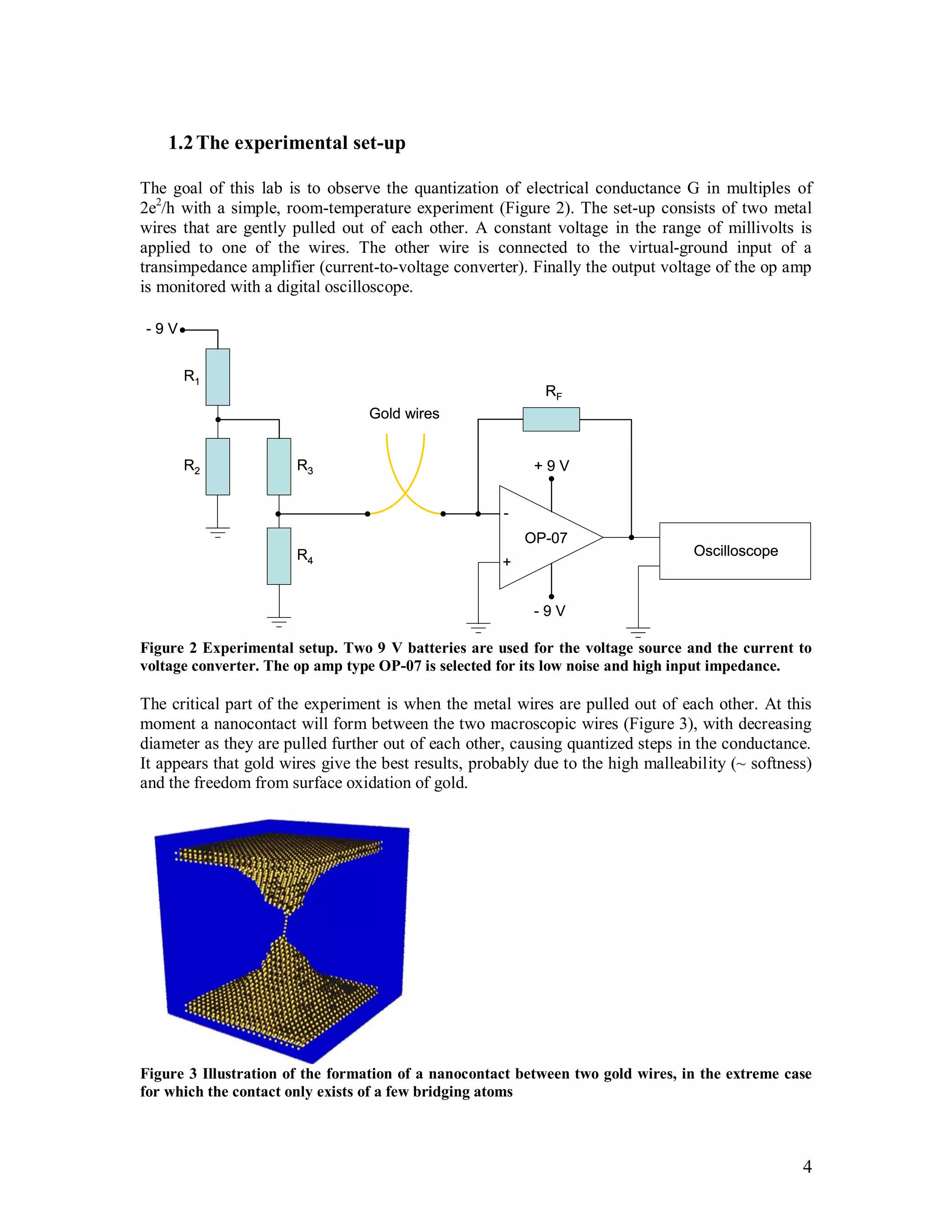
1. Introduction
The first experiment on ballistic transport goes back to 1965, when Yuri Sharvin (Moscow) used
a pair of point contacts to inject and detect a beam of electrons in a single-crystalline metal. In his
experiment he used a two-dimensional electron gas in a GaAs-AlGaAs heterojunction to create a
quantum point contact. In 1988, the Delft-Philips and Cambridge groups reported the observation
of a sequence of steps in the conductance of a constriction in a 2D electron gas, as its width W
was varied by means of the voltage on the gate. The steps are near integer multiples of 2e²/h
1/13k. A far more simple experiment however, was proposed by Costa-Krämer et al [1] in
1995, placing in contact two metallic wires and separating them, while forming a ballistic
nanowire in between. It is on the latter experiment that this lab is based.
1.1 The physics of quantized conductance
Let us first consider the conductance of a one-dimensional wire of length L. The conductance is
the reverse of the resistance and is equal to the current divided by the voltage
V
I
R
G
1 (1)
.
The current is given by the following formula
L
veN
I (2)
for which v is the velocity of the electrons, e is the elementary charge (= absolute value of the
charge of an electron) and N is the total number of electrons that contribute to the current. The
drop in potential energy for 1 electron going from one end of the wire to the other is
eVE (3)
.
Substituting both equation (2) and (3) in equation (1), gives
EL
Nve
G
2
(4)
.
The problem reduces now to computing the number of contributing electrons N. At each of the
two terminals (call them A and B), which are connected to the two ends of the one-dimensional
wire, the quantum states are filled up to the Fermi energy, EFA respectively EFB, with two
electrons per state (Pauli exclusion principle). At terminal A, the Fermi energy level is higher by
E due to the applied voltage and this causes the current flow. So from terminal A all the
electrons that occupy the states in a range E below EFA, can flow to unoccupied states in
terminal B. The number of contributing electrons N equals twice the number of quantum states S
in [EFA - E, EFA].
Recall from chapter 1, section 1.7, that for particles in a one-dimensional box of length L, the
wavenumber is restricted to values
L
n
kn
2
...2,1,0 n (5)
and thus the de Broglie wavelength of an electron can only take on discrete values
n
L
n ...2,1,0 n (6)
.
The formula of the velocity of an electron is](https://image.slidesharecdn.com/0494d061-9803-4afc-ba2a-2339f3867202-150505090305-conversion-gate02/75/QC-2-2048.jpg)
![3
m
h
m
p
v
(7)
,
with m the effective mass of an electron, so the electron velocity in a one-dimensional wire can
only have the following discrete values
Lm
nh
vn ...2,1,0 n (8)
.
The number of electrons N, which occupy the S states in [EFA - E, EFA], travel at different
velocities depending on the quantum state. This velocity range
Lm
Sh
Lm
xh
Lm
hSx
vvv xSx
)( (9)
converts to a range of kinetic energy
L
vSh
vmv
vvm
Ekin
2
2 (10)
.
The potential energy E, provided to the system by the applied voltage, equals the kinetic energy
Ekin of the electrons that propagate through the wire. Isolating the number of quantum states S
from (10), results in
vh
EL
vh
LE
S kin
(11)
vh
EL
SN
2
2 (12)
.
Substituting the number of contributing electrons N (12) into equation (4) immediately gives
h
e
G
2
2
(13)
.
Now consider the conductance of a nanosized contact, like we will make in this experiment. As
seen in Figure 1, a nanosized contact acts as a ballistic conductor, for which the scattering of
electrons at the sample boundaries limits the current, rather than impurity scattering. Although
one might expect the current I to be infinitely large in the ballistic transport regime, it is actually
finite, because electrons are scattered back at the entrance of the constriction.
The nanocontact acts like a waveguide for electrons, with a finite, integer number of occupied
modes “above cutoff”, that are able to propagate*
. As the size of the contact is increased
(decreased), the number of allowed modes increases (decreases) discontinuously. For each
allowed mode, the nanosized contact acts like a one-dimensional wire with conductance G =
2e2
/h.
Figure 1 Electron trajectories characteristic for diffusive
(l < W, L), quasi-ballistic (W < l < L) and ballistic (W, L
< l) transport regimes with l the electron mean free
path, W the width and L the length of the channel
*
This is a rather rough argument. For a rigorous explanation read C. W. J. Beenakker and H. van Houten,
“Quantum Transport in Semiconductor nanostructures,” Solid State Phys. 44, 1-228 (1991).](https://image.slidesharecdn.com/0494d061-9803-4afc-ba2a-2339f3867202-150505090305-conversion-gate02/75/QC-3-2048.jpg)


The document describes an experiment to observe quantized conductance in gold wire nanocontacts. A circuit is constructed using batteries, resistors, and an operational amplifier to apply a voltage between two gold wires and measure the current as the wires are slowly separated. Quantized steps in the conductance are expected as the contact width decreases to the nanoscale due to the quantum confinement of electron transport. Students will perform the experiment, record oscilloscope measurements of the conductance steps for both gold and solder wires, and analyze the results to determine if they match theoretical predictions.


