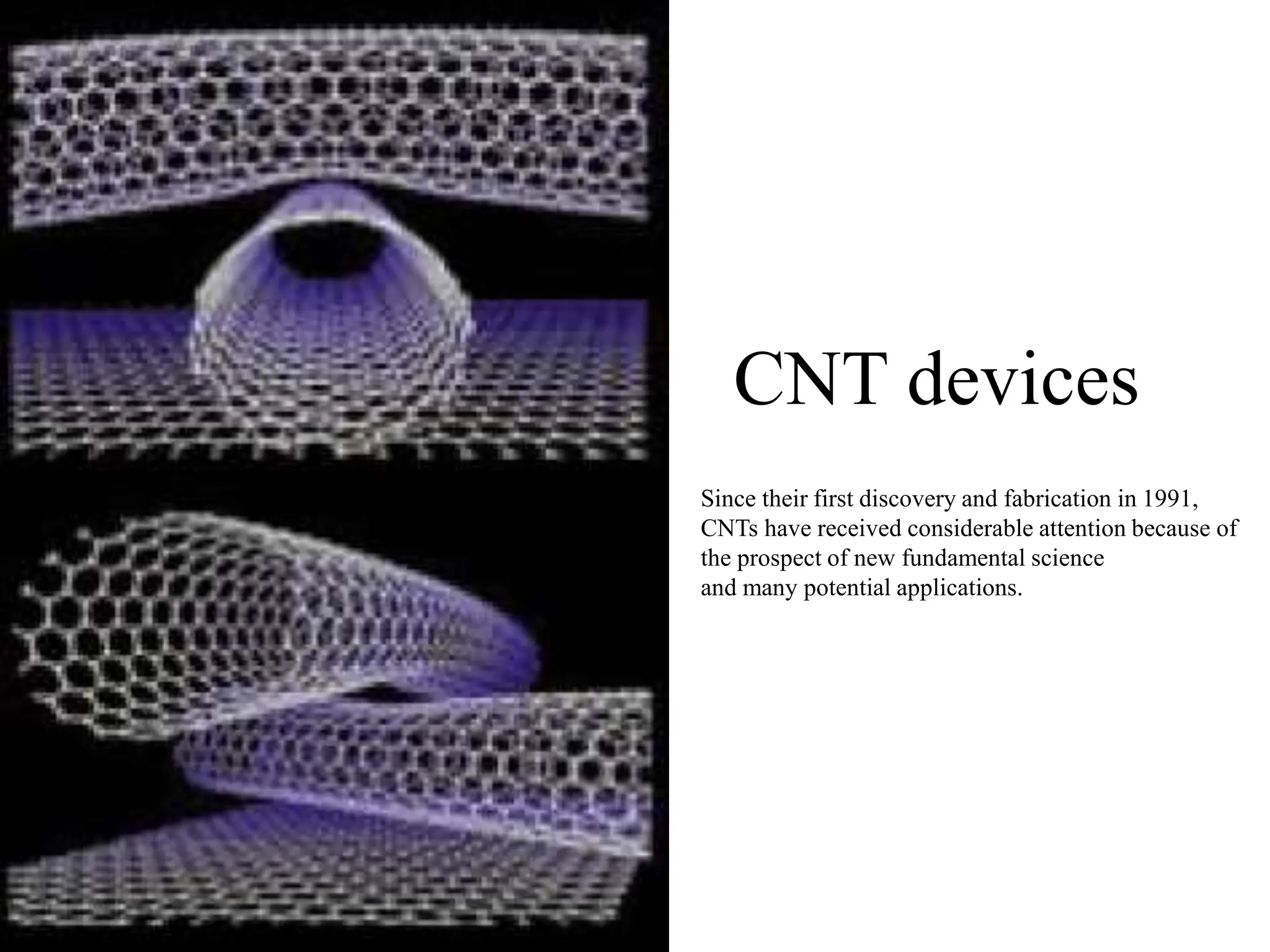
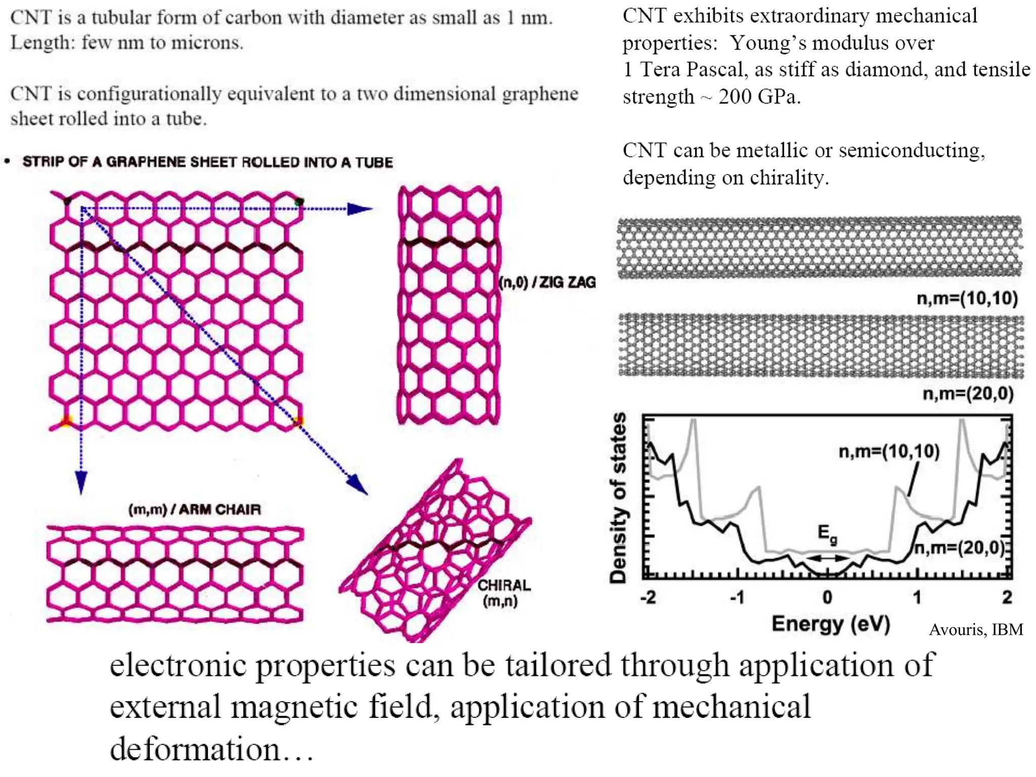
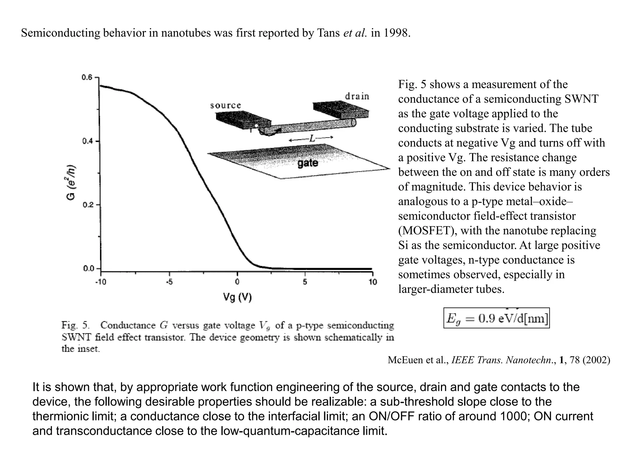
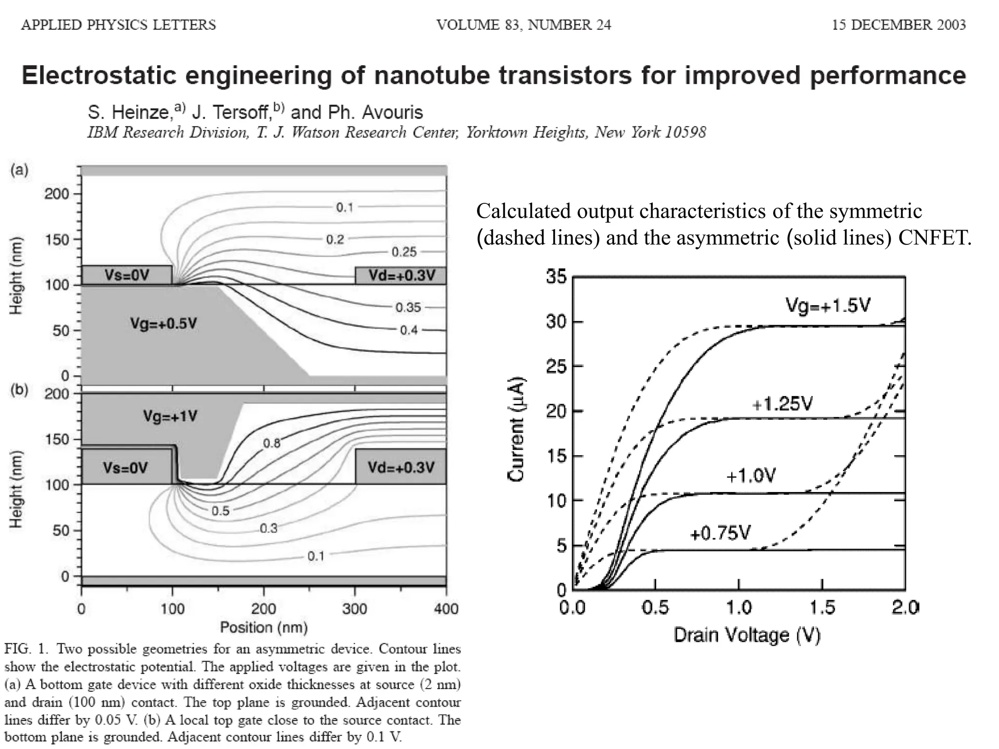
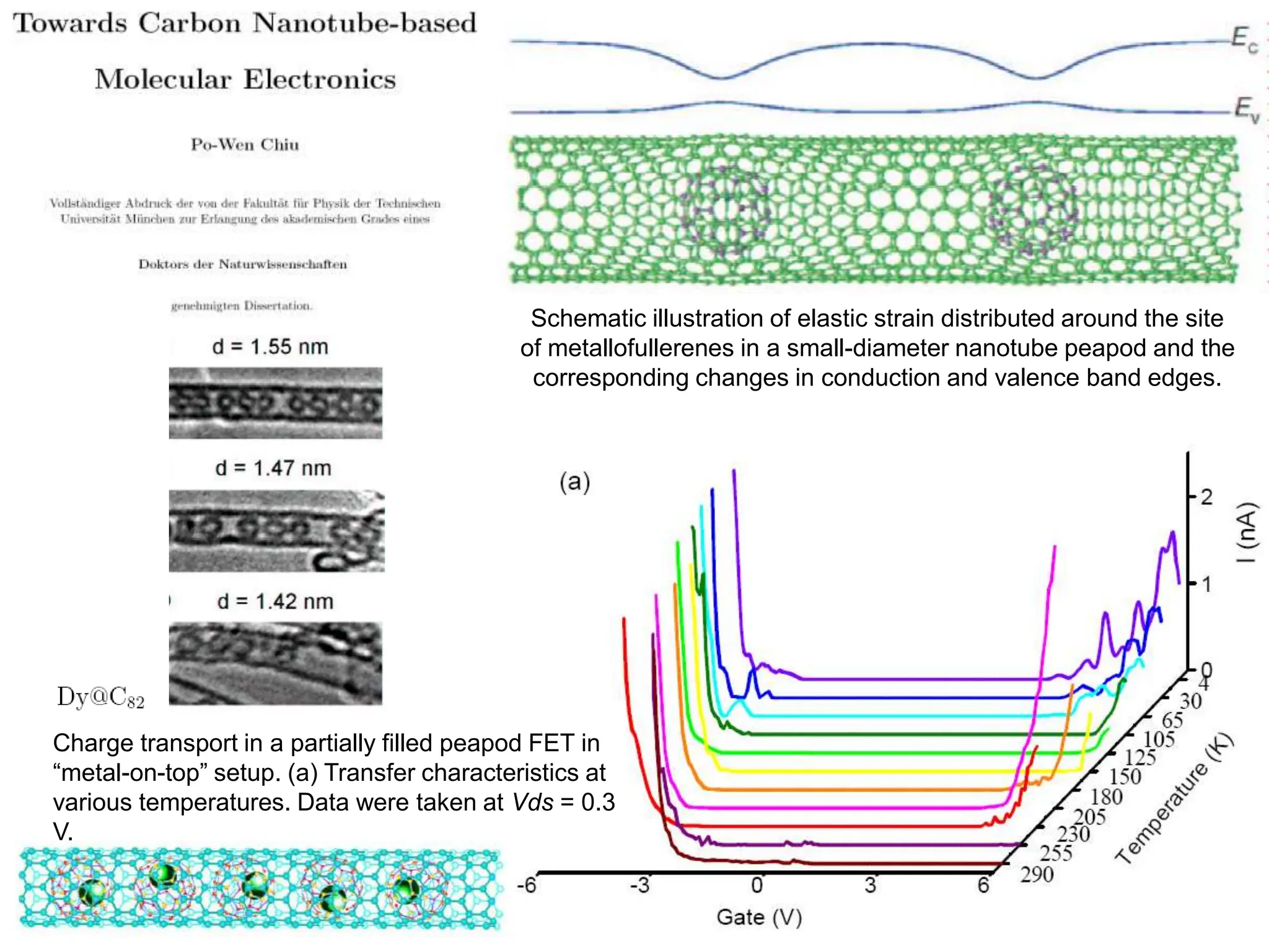
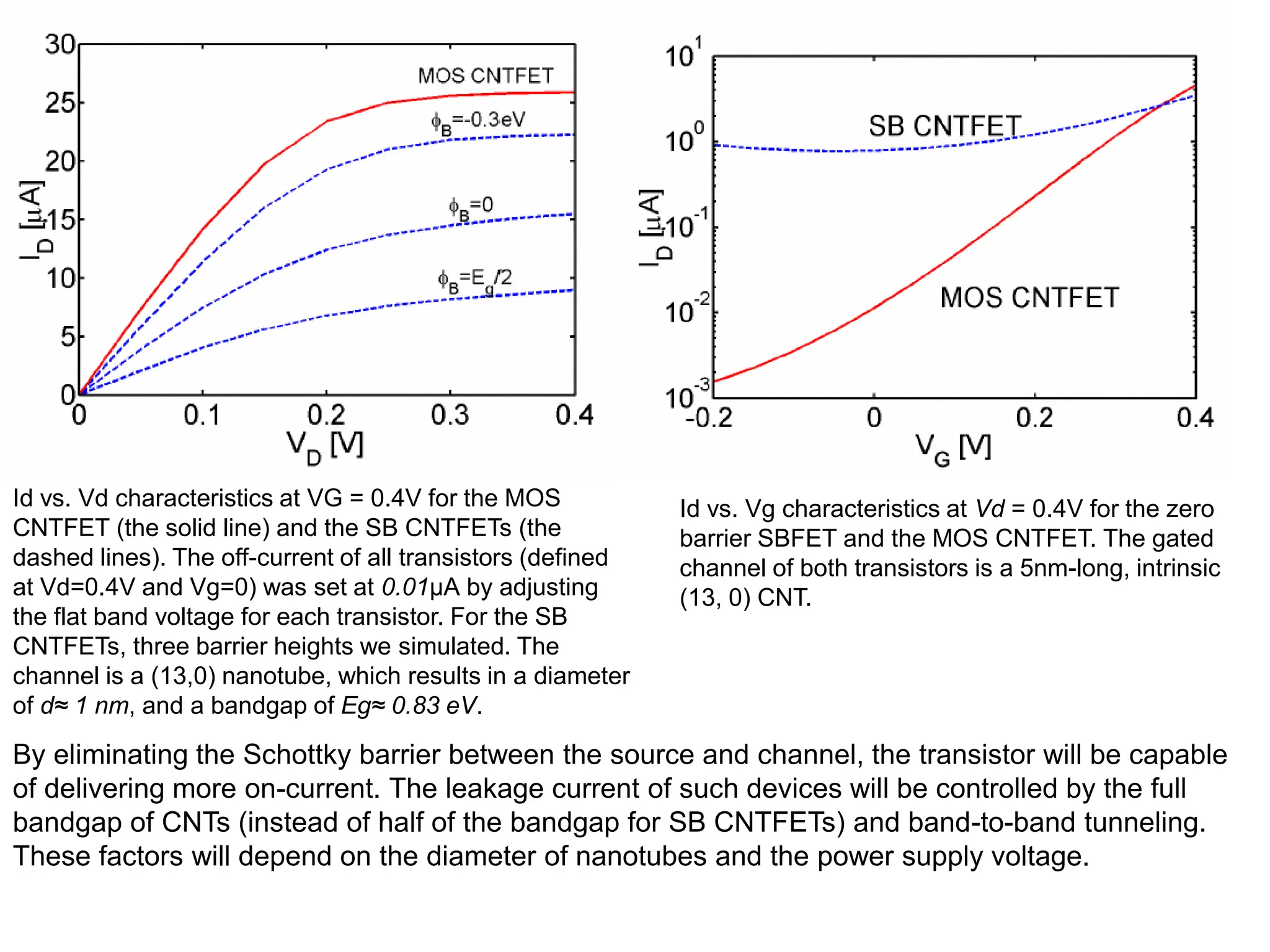
SlideShare a Scribd company logo
1 of 25
CNT devices
Since their first discovery and fabrication in 1991,
CNTs have received considerable attention because of
the prospect of new fundamental science
and many potential applications.
Avouris, IBM
Stretching And confined deformation
Strain of less than 1% results in
the CNT changing from metal to
semiconductor.
Twisting and bending
The encapsulated fullerenes can rotate
freely in the space of a (10, 10) tube at
room temperature, and the rotation of
fullerenes will affect C60@(10, 10)
peapod electronic properties significantly;
generally, orientational disorderwill
remove the sharp features of the average
density of states (DOS). However, the
rotation of fullerenes cannot induce a
metal–insulator transition. Unlike the
multicarrier metallic C60@(10, 10)
peapod, the C60@(17, 0) peapod is a
semiconductor, and the effects of the
encapsulated fullerenes on tube valence
bands and conduction bands are
asymmetrical.
The distances between the centres of the
fullerenes are 0.984 and 1.278 nm for the
C60@(10, 10) peapod and C60@(17, 0)
peapod, respectively.
Peapods
J. Chen, and J. Dong, J. Phys. Condens. Matter, 16, 1401 (2
It is shown that, by appropriate work function engineering of the source, drain and gate contacts to the
device, the following desirable properties should be realizable: a sub-threshold slope close to the
thermionic limit; a conductance close to the interfacial limit; an ON/OFF ratio of around 1000; ON current
and transconductance close to the low-quantum-capacitance limit.
Semiconducting behavior in nanotubes was first reported by Tans et al. in 1998.
Fig. 5 shows a measurement of the
conductance of a semiconducting SWNT
as the gate voltage applied to the
conducting substrate is varied. The tube
conducts at negative Vg and turns off with
a positive Vg. The resistance change
between the on and off state is many orders
of magnitude. This device behavior is
analogous to a p-type metal–oxide–
semiconductor field-effect transistor
(MOSFET), with the nanotube replacing
Si as the semiconductor. At large positive
gate voltages, n-type conductance is
sometimes observed, especially in
larger-diameter tubes.
McEuen et al., IEEE Trans. Nanotechn., 1, 78 (2002)
Semiconducting nanotubes are typically p-type at Vg=0 because of the contacts and also because chemical species,
particularly oxygen, adsorb on the tube and act as weak p-type dopants. Experiments have shown that changing a
tube’s chemical environment can change this doping level—shifting the voltage at which the device turns on by a
significant amount. This has spurred interest in nanotubes as chemical sensors.
Adsorbate doping can be a problem for reproducible device behavior, however.
Controlled chemical doping of tubes, both p- and n-type, has been accomplished in a number of ways. N-type doping
was first done using alkali metals that donate electrons to the tube. This has been used to create n-type transistors, p-n
junctions, and p-n-p devices. Alkali metals are not air-stable, however, so other techniques are under development,
such as using polymers for charge-transfer doping
Scattering sites in nanotubes:
I–V characteristics at different Vgs for a p-
type SWNT FET utilizing an electrolyte gate
in order to improve gate efficiency.
McEuen et al., IEEE Trans. Nanotechn., 1, 78 (2002)
Implying a mean-free path of approx. 700 nm.
Maximum transconductance dI/dVg=20uA/V at Vg=-0.9V.
Normalizing this to the device width of ~2nm: 10mS/um.
Bottom - gated CNT FET
Calculated conductance vs gate voltage at room temperature, varying
(a) the work function of the metal electrode, and (b) doping of the NT.
In (a) the work function of the metal electrode is changed by -0.2 eV (red
dashed), -0.1 eV (orange dashed), 0 eV (green), +0.1 eV (light blue),
and +0.2 eV (blue), from left to right, respectively. In (b) the doping
atomic fraction is n-type 0.001 (red), 0.0005 (orange), and 0.0001
(green), and p-type 0.0001 (blue dashed), from left to right, respectively.
Thus the gate field induces switching by modulating the contact resistance (the
junction barriers). Oxygen adsorption at the junctions modifies the barriers (i.e.
the local band-bending of the CNT) and affects the injection of carriers (holes
or electrons).
The inverse subthreshold slope, which is a measure of the
efficiency of the gate field in turning on the device,
decreases with a decrease in gate oxide thickness. This
behavior cannot be explained by conventional field-effect
transistor models, and has in fact been shown to be a result
of the presence of Schottky barriers at the metal/nanotube
interface at the source and drain.
There is a clear difference in the inverse subthreshold slope for the case of sweeping all gate segments together (S=400
mV/dec) versus sweeping only the inner segments (S=180 mV/dec). We attribute the observed change in S to a change from
Schottky barrier modulation to bulk switching. (b) shows linear plots of the subthreshold portion (where the current is
dominated by carrier density) of the transfer characteristics when the inner gate segments are swept together or separately.
The current nearly identical, despite the fact that the effective gate lengths differ by a factor of 1.6 . This is in contrast to the
expected behavior of diffusive transport, where the current varies inversely with the gate length.
Calculated output characteristics of the symmetric
(dashed lines) and the asymmetric (solid lines) CNFET.
We have introduced nanotemplate to control selective growth,
length and diameter of CNT. Ohmic contact of the CNT/metal
interface was formed by rapid thermal annealing (RTA).
Diameter control and surface modification of CNT open the
possibility to energy band gap modulation.
Diode-like rectifying behavior was observed in a CNx /C multiwalled
nanotube due to its being one half doped with nitrogen.
FETs based on an individual CNx /C nanotube were fabricated by focused
ion-beam technology. The nanotube transistors exhibited n-type
semiconductor characteristics, and the conductance of nanotube FETs can
be modulated more than four orders of magnitude at room temperature.
The electron mobility of a CNx /C NT FET estimated from its
transconductance was as high as 3840 cm2/Vs. The n-type gate
modulation could be explained as due the effect of bending of the valence
band in the Schottky-barrier junction.
CNTs doped with fullerenes inside nanotubes (so-called peapods) are interesting materials for novel CNT FET
channels. Transport properties of various peapods such as C60-, Gd@C82-, and Ti2@C92-peapods have been
studied by measuring FET I-V characteristics. Metallofulleren peapod FETs exhibited ambipolar behavior both
p- and n-type characteristics by changing the gate voltage, whereas C60-peapod FETs showed unipolar p-type
characteristics similar to the FETs of intact single-walled nanotubes. This difference can be explained in terms
of a bandgap narrowing of the single-walled nanotube due to the incorporation of metallofullerenes. The
bandgap narrowing was large in the peapods of metallofullerene, where more electrons are transferred from
encapsulated metal atoms to the fullerene cages.
The entrapped fullerene molecules are capable of
modifying the electronic structure of the host tube. It is,
therefore, anticipated that the encapsulation of fullerene
molecules can play a role in band gap engineering in
nanotubes and hence that peapods may generate
conceptually novel molecular devices.
Schematic illustration of elastic strain distributed around the site
of metallofullerenes in a small-diameter nanotube peapod and the
corresponding changes in conduction and valence band edges.
Charge transport in a partially filled peapod FET in
“metal-on-top” setup. (a) Transfer characteristics at
various temperatures. Data were taken at Vds = 0.3
V.
CNT junction
Current vs. voltage characteristics of an all-carbon transistor
with semiconducting nanotube as channel, with different voltag
at the carbon gate. The back gate is kept at 0 V. The measurem
were carried out at 4 K.
The band profile of the SB CNTFET at the minimal leakage bias (VG=0V) for VD=0.6V. The band profile of
the MOS CNTFET when the source-drain current is low. (VD=0.6V and VG=-0.3V). The channel is a (13,0)
nanotube.
Ambipolar conduction leads to a large
leakage current that exponentially
increases with the power supply voltage,
especially when the tube diameter is
large. An asymmetric gate oxide SB
CNTFET has been proposed as a means
of suppressing ambipolar conduction. SB
CNTFETs of any type, however, will likely
suffer from the need to place the gate
electrode close to the source (which
increases parasitic capacitance) and
metal-induced gap states, which
increase source to drain tunneling and
limit the minimum channel length.
Id vs. Vd characteristics at VG = 0.4V for the MOS
CNTFET (the solid line) and the SB CNTFETs (the
dashed lines). The off-current of all transistors (defined
at Vd=0.4V and Vg=0) was set at 0.01µA by adjusting
the flat band voltage for each transistor. For the SB
CNTFETs, three barrier heights we simulated. The
channel is a (13,0) nanotube, which results in a diameter
of d≈ 1 nm, and a bandgap of Eg≈ 0.83 eV.
Id vs. Vg characteristics at Vd = 0.4V for the zero
barrier SBFET and the MOS CNTFET. The gated
channel of both transistors is a 5nm-long, intrinsic
(13, 0) CNT.
By eliminating the Schottky barrier between the source and channel, the transistor will be capable
of delivering more on-current. The leakage current of such devices will be controlled by the full
bandgap of CNTs (instead of half of the bandgap for SB CNTFETs) and band-to-band tunneling.
These factors will depend on the diameter of nanotubes and the power supply voltage.

More Related Content

Similar to CNT as Field Effect Transistor application

Analytical Modeling of Tunneling Field Effect Transistor (TFET)
Analytical Modeling of Tunneling Field Effect Transistor (TFET)Analytical Modeling of Tunneling Field Effect Transistor (TFET)
Analytical Modeling of Tunneling Field Effect Transistor (TFET)Abu Obayda
 
ECE 6030 Device Electronics.docx
ECE 6030 Device Electronics.docxECE 6030 Device Electronics.docx
ECE 6030 Device Electronics.docxwrite31
 
Nanoelectronics Final
Nanoelectronics FinalNanoelectronics Final
Nanoelectronics Finalshikha2510
 
Performance analysis of cntfet and mosfet focusing channel length, carrier mo...
Performance analysis of cntfet and mosfet focusing channel length, carrier mo...Performance analysis of cntfet and mosfet focusing channel length, carrier mo...
Performance analysis of cntfet and mosfet focusing channel length, carrier mo...IJAMSE Journal
 
Mfsfet metal ferroelectric semiconductor field effect transistor
Mfsfet  metal ferroelectric semiconductor field effect transistorMfsfet  metal ferroelectric semiconductor field effect transistor
Mfsfet metal ferroelectric semiconductor field effect transistordhanusharavindhan
 
Transistor and it's working principle
Transistor and it's working principleTransistor and it's working principle
Transistor and it's working principleEkram Bin Mamun
 
transistoranditsworkingprinciple-160427150207 (1).pdf
transistoranditsworkingprinciple-160427150207 (1).pdftransistoranditsworkingprinciple-160427150207 (1).pdf
transistoranditsworkingprinciple-160427150207 (1).pdfrahulreddy773814
 
Poster_STEM_Research
Poster_STEM_ResearchPoster_STEM_Research
Poster_STEM_ResearchJada Gray
 
Welcome to International Journal of Engineering Research and Development (IJERD)
Welcome to International Journal of Engineering Research and Development (IJERD)Welcome to International Journal of Engineering Research and Development (IJERD)
Welcome to International Journal of Engineering Research and Development (IJERD)IJERD Editor
 
Carbon Nano tubes and its Applications in the Field of Electronics and Comput...
Carbon Nano tubes and its Applications in the Field of Electronics and Comput...Carbon Nano tubes and its Applications in the Field of Electronics and Comput...
Carbon Nano tubes and its Applications in the Field of Electronics and Comput...ijsrd.com
 
A Comparative Study on Carbon Nanotube MOSFET, Silicon Nanowire MOSFET and Si...
A Comparative Study on Carbon Nanotube MOSFET, Silicon Nanowire MOSFET and Si...A Comparative Study on Carbon Nanotube MOSFET, Silicon Nanowire MOSFET and Si...
A Comparative Study on Carbon Nanotube MOSFET, Silicon Nanowire MOSFET and Si...Mukit Ahmed Chowdhury
 
Modeling and Structure Optimization of Tapped Transformer
Modeling and Structure Optimization of Tapped Transformer Modeling and Structure Optimization of Tapped Transformer
Modeling and Structure Optimization of Tapped Transformer IJECEIAES
 
Modeling and Structure Optimization of Tapped Transformer
Modeling and Structure Optimization of Tapped Transformer Modeling and Structure Optimization of Tapped Transformer
Modeling and Structure Optimization of Tapped Transformer Yayah Zakaria
 
Carbonnanotubes
CarbonnanotubesCarbonnanotubes
CarbonnanotubesHoang Tien
 
Abstract_CNTFET_2015_STEM-Day
Abstract_CNTFET_2015_STEM-DayAbstract_CNTFET_2015_STEM-Day
Abstract_CNTFET_2015_STEM-DayJada Gray
 

Similar to CNT as Field Effect Transistor application (20)

CNFET Technology
CNFET TechnologyCNFET Technology
CNFET Technology
 
Analytical Modeling of Tunneling Field Effect Transistor (TFET)
Analytical Modeling of Tunneling Field Effect Transistor (TFET)Analytical Modeling of Tunneling Field Effect Transistor (TFET)
Analytical Modeling of Tunneling Field Effect Transistor (TFET)
 
ECE 6030 Device Electronics.docx
ECE 6030 Device Electronics.docxECE 6030 Device Electronics.docx
ECE 6030 Device Electronics.docx
 
Nanoelectronics Final
Nanoelectronics FinalNanoelectronics Final
Nanoelectronics Final
 
Cnt flow-sensorss
Cnt flow-sensorssCnt flow-sensorss
Cnt flow-sensorss
 
Performance analysis of cntfet and mosfet focusing channel length, carrier mo...
Performance analysis of cntfet and mosfet focusing channel length, carrier mo...Performance analysis of cntfet and mosfet focusing channel length, carrier mo...
Performance analysis of cntfet and mosfet focusing channel length, carrier mo...
 
Carbon nanotube
Carbon nanotubeCarbon nanotube
Carbon nanotube
 
Master's Thesis Presentation
Master's Thesis PresentationMaster's Thesis Presentation
Master's Thesis Presentation
 
Mfsfet metal ferroelectric semiconductor field effect transistor
Mfsfet  metal ferroelectric semiconductor field effect transistorMfsfet  metal ferroelectric semiconductor field effect transistor
Mfsfet metal ferroelectric semiconductor field effect transistor
 
Transistor and it's working principle
Transistor and it's working principleTransistor and it's working principle
Transistor and it's working principle
 
transistoranditsworkingprinciple-160427150207 (1).pdf
transistoranditsworkingprinciple-160427150207 (1).pdftransistoranditsworkingprinciple-160427150207 (1).pdf
transistoranditsworkingprinciple-160427150207 (1).pdf
 
Poster_STEM_Research
Poster_STEM_ResearchPoster_STEM_Research
Poster_STEM_Research
 
Welcome to International Journal of Engineering Research and Development (IJERD)
Welcome to International Journal of Engineering Research and Development (IJERD)Welcome to International Journal of Engineering Research and Development (IJERD)
Welcome to International Journal of Engineering Research and Development (IJERD)
 
Carbonnanotubes
Carbonnanotubes Carbonnanotubes
Carbonnanotubes
 
Carbon Nano tubes and its Applications in the Field of Electronics and Comput...
Carbon Nano tubes and its Applications in the Field of Electronics and Comput...Carbon Nano tubes and its Applications in the Field of Electronics and Comput...
Carbon Nano tubes and its Applications in the Field of Electronics and Comput...
 
A Comparative Study on Carbon Nanotube MOSFET, Silicon Nanowire MOSFET and Si...
A Comparative Study on Carbon Nanotube MOSFET, Silicon Nanowire MOSFET and Si...A Comparative Study on Carbon Nanotube MOSFET, Silicon Nanowire MOSFET and Si...
A Comparative Study on Carbon Nanotube MOSFET, Silicon Nanowire MOSFET and Si...
 
Modeling and Structure Optimization of Tapped Transformer
Modeling and Structure Optimization of Tapped Transformer Modeling and Structure Optimization of Tapped Transformer
Modeling and Structure Optimization of Tapped Transformer
 
Modeling and Structure Optimization of Tapped Transformer
Modeling and Structure Optimization of Tapped Transformer Modeling and Structure Optimization of Tapped Transformer
Modeling and Structure Optimization of Tapped Transformer
 
Carbonnanotubes
CarbonnanotubesCarbonnanotubes
Carbonnanotubes
 
Abstract_CNTFET_2015_STEM-Day
Abstract_CNTFET_2015_STEM-DayAbstract_CNTFET_2015_STEM-Day
Abstract_CNTFET_2015_STEM-Day
 

Recently uploaded

Russian Call Girls Kolkata Chhaya 🤌 8250192130 🚀 Vip Call Girls Kolkata
Russian Call Girls Kolkata Chhaya 🤌  8250192130 🚀 Vip Call Girls KolkataRussian Call Girls Kolkata Chhaya 🤌  8250192130 🚀 Vip Call Girls Kolkata
Russian Call Girls Kolkata Chhaya 🤌 8250192130 🚀 Vip Call Girls Kolkataanamikaraghav4
 
Low Rate Call Girls Nashik Vedika 7001305949 Independent Escort Service Nashik
Low Rate Call Girls Nashik Vedika 7001305949 Independent Escort Service NashikLow Rate Call Girls Nashik Vedika 7001305949 Independent Escort Service Nashik
Low Rate Call Girls Nashik Vedika 7001305949 Independent Escort Service NashikCall Girls in Nagpur High Profile
 
Kalyan callg Girls, { 07738631006 } || Call Girl In Kalyan Women Seeking Men ...
Kalyan callg Girls, { 07738631006 } || Call Girl In Kalyan Women Seeking Men ...Kalyan callg Girls, { 07738631006 } || Call Girl In Kalyan Women Seeking Men ...
Kalyan callg Girls, { 07738631006 } || Call Girl In Kalyan Women Seeking Men ...Pooja Nehwal
 
《伯明翰城市大学毕业证成绩单购买》学历证书学位证书区别《复刻原版1:1伯明翰城市大学毕业证书|修改BCU成绩单PDF版》Q微信741003700《BCU学...
《伯明翰城市大学毕业证成绩单购买》学历证书学位证书区别《复刻原版1:1伯明翰城市大学毕业证书|修改BCU成绩单PDF版》Q微信741003700《BCU学...《伯明翰城市大学毕业证成绩单购买》学历证书学位证书区别《复刻原版1:1伯明翰城市大学毕业证书|修改BCU成绩单PDF版》Q微信741003700《BCU学...
《伯明翰城市大学毕业证成绩单购买》学历证书学位证书区别《复刻原版1:1伯明翰城市大学毕业证书|修改BCU成绩单PDF版》Q微信741003700《BCU学...ur8mqw8e
 
presentation about microsoft power point
presentation about microsoft power pointpresentation about microsoft power point
presentation about microsoft power pointchhavia330
 
如何办理(Adelaide毕业证)阿德莱德大学毕业证成绩单Adelaide学历认证真实可查
如何办理(Adelaide毕业证)阿德莱德大学毕业证成绩单Adelaide学历认证真实可查如何办理(Adelaide毕业证)阿德莱德大学毕业证成绩单Adelaide学历认证真实可查
如何办理(Adelaide毕业证)阿德莱德大学毕业证成绩单Adelaide学历认证真实可查awo24iot
 
Call Girls Service Kolkata Aishwarya 🤌 8250192130 🚀 Vip Call Girls Kolkata
Call Girls Service Kolkata Aishwarya 🤌  8250192130 🚀 Vip Call Girls KolkataCall Girls Service Kolkata Aishwarya 🤌  8250192130 🚀 Vip Call Girls Kolkata
Call Girls Service Kolkata Aishwarya 🤌 8250192130 🚀 Vip Call Girls Kolkataanamikaraghav4
 
VIP Call Girls Hitech City ( Hyderabad ) Phone 8250192130 | ₹5k To 25k With R...
VIP Call Girls Hitech City ( Hyderabad ) Phone 8250192130 | ₹5k To 25k With R...VIP Call Girls Hitech City ( Hyderabad ) Phone 8250192130 | ₹5k To 25k With R...
VIP Call Girls Hitech City ( Hyderabad ) Phone 8250192130 | ₹5k To 25k With R...Suhani Kapoor
 
High Profile Call Girls In Andheri 7738631006 Call girls in mumbai Mumbai ...
High Profile Call Girls In Andheri 7738631006 Call girls in mumbai  Mumbai ...High Profile Call Girls In Andheri 7738631006 Call girls in mumbai  Mumbai ...
High Profile Call Girls In Andheri 7738631006 Call girls in mumbai Mumbai ...Pooja Nehwal
 
VIP Call Girl Saharanpur Aashi 8250192130 Independent Escort Service Saharanpur
VIP Call Girl Saharanpur Aashi 8250192130 Independent Escort Service SaharanpurVIP Call Girl Saharanpur Aashi 8250192130 Independent Escort Service Saharanpur
VIP Call Girl Saharanpur Aashi 8250192130 Independent Escort Service SaharanpurSuhani Kapoor
 
Develop Keyboard Skill.pptx er power point
Develop Keyboard Skill.pptx er power pointDevelop Keyboard Skill.pptx er power point
Develop Keyboard Skill.pptx er power pointGetawu
 
Thane Escorts, (Pooja 09892124323), Thane Call Girls
Thane Escorts, (Pooja 09892124323), Thane Call GirlsThane Escorts, (Pooja 09892124323), Thane Call Girls
Thane Escorts, (Pooja 09892124323), Thane Call GirlsPooja Nehwal
 
Call Girls In Andheri East Call 9892124323 Book Hot And Sexy Girls,
Call Girls In Andheri East Call 9892124323 Book Hot And Sexy Girls,Call Girls In Andheri East Call 9892124323 Book Hot And Sexy Girls,
Call Girls In Andheri East Call 9892124323 Book Hot And Sexy Girls,Pooja Nehwal
 
Call Girls Kothrud Call Me 7737669865 Budget Friendly No Advance Booking
Call Girls Kothrud Call Me 7737669865 Budget Friendly No Advance BookingCall Girls Kothrud Call Me 7737669865 Budget Friendly No Advance Booking
Call Girls Kothrud Call Me 7737669865 Budget Friendly No Advance Bookingroncy bisnoi
 
Call Girls in Vashi Escorts Services - 7738631006
Call Girls in Vashi Escorts Services - 7738631006Call Girls in Vashi Escorts Services - 7738631006
Call Girls in Vashi Escorts Services - 7738631006Pooja Nehwal
 
Top Rated Pune Call Girls Katraj ⟟ 6297143586 ⟟ Call Me For Genuine Sex Serv...
Top Rated  Pune Call Girls Katraj ⟟ 6297143586 ⟟ Call Me For Genuine Sex Serv...Top Rated  Pune Call Girls Katraj ⟟ 6297143586 ⟟ Call Me For Genuine Sex Serv...
Top Rated Pune Call Girls Katraj ⟟ 6297143586 ⟟ Call Me For Genuine Sex Serv...Call Girls in Nagpur High Profile
 
Dubai Call Girls O528786472 Call Girls In Dubai Wisteria
Dubai Call Girls O528786472 Call Girls In Dubai WisteriaDubai Call Girls O528786472 Call Girls In Dubai Wisteria
Dubai Call Girls O528786472 Call Girls In Dubai WisteriaUnited Arab Emirates
 
9004554577, Get Adorable Call Girls service. Book call girls & escort service...
9004554577, Get Adorable Call Girls service. Book call girls & escort service...9004554577, Get Adorable Call Girls service. Book call girls & escort service...
9004554577, Get Adorable Call Girls service. Book call girls & escort service...Pooja Nehwal
 
(ZARA) Call Girls Jejuri ( 7001035870 ) HI-Fi Pune Escorts Service
(ZARA) Call Girls Jejuri ( 7001035870 ) HI-Fi Pune Escorts Service(ZARA) Call Girls Jejuri ( 7001035870 ) HI-Fi Pune Escorts Service
(ZARA) Call Girls Jejuri ( 7001035870 ) HI-Fi Pune Escorts Serviceranjana rawat
 

Recently uploaded (20)

Russian Call Girls Kolkata Chhaya 🤌 8250192130 🚀 Vip Call Girls Kolkata
Russian Call Girls Kolkata Chhaya 🤌  8250192130 🚀 Vip Call Girls KolkataRussian Call Girls Kolkata Chhaya 🤌  8250192130 🚀 Vip Call Girls Kolkata
Russian Call Girls Kolkata Chhaya 🤌 8250192130 🚀 Vip Call Girls Kolkata
 
Low Rate Call Girls Nashik Vedika 7001305949 Independent Escort Service Nashik
Low Rate Call Girls Nashik Vedika 7001305949 Independent Escort Service NashikLow Rate Call Girls Nashik Vedika 7001305949 Independent Escort Service Nashik
Low Rate Call Girls Nashik Vedika 7001305949 Independent Escort Service Nashik
 
Kalyan callg Girls, { 07738631006 } || Call Girl In Kalyan Women Seeking Men ...
Kalyan callg Girls, { 07738631006 } || Call Girl In Kalyan Women Seeking Men ...Kalyan callg Girls, { 07738631006 } || Call Girl In Kalyan Women Seeking Men ...
Kalyan callg Girls, { 07738631006 } || Call Girl In Kalyan Women Seeking Men ...
 
《伯明翰城市大学毕业证成绩单购买》学历证书学位证书区别《复刻原版1:1伯明翰城市大学毕业证书|修改BCU成绩单PDF版》Q微信741003700《BCU学...
《伯明翰城市大学毕业证成绩单购买》学历证书学位证书区别《复刻原版1:1伯明翰城市大学毕业证书|修改BCU成绩单PDF版》Q微信741003700《BCU学...《伯明翰城市大学毕业证成绩单购买》学历证书学位证书区别《复刻原版1:1伯明翰城市大学毕业证书|修改BCU成绩单PDF版》Q微信741003700《BCU学...
《伯明翰城市大学毕业证成绩单购买》学历证书学位证书区别《复刻原版1:1伯明翰城市大学毕业证书|修改BCU成绩单PDF版》Q微信741003700《BCU学...
 
presentation about microsoft power point
presentation about microsoft power pointpresentation about microsoft power point
presentation about microsoft power point
 
如何办理(Adelaide毕业证)阿德莱德大学毕业证成绩单Adelaide学历认证真实可查
如何办理(Adelaide毕业证)阿德莱德大学毕业证成绩单Adelaide学历认证真实可查如何办理(Adelaide毕业证)阿德莱德大学毕业证成绩单Adelaide学历认证真实可查
如何办理(Adelaide毕业证)阿德莱德大学毕业证成绩单Adelaide学历认证真实可查
 
🔝 9953056974🔝 Delhi Call Girls in Ajmeri Gate
🔝 9953056974🔝 Delhi Call Girls in Ajmeri Gate🔝 9953056974🔝 Delhi Call Girls in Ajmeri Gate
🔝 9953056974🔝 Delhi Call Girls in Ajmeri Gate
 
Call Girls Service Kolkata Aishwarya 🤌 8250192130 🚀 Vip Call Girls Kolkata
Call Girls Service Kolkata Aishwarya 🤌  8250192130 🚀 Vip Call Girls KolkataCall Girls Service Kolkata Aishwarya 🤌  8250192130 🚀 Vip Call Girls Kolkata
Call Girls Service Kolkata Aishwarya 🤌 8250192130 🚀 Vip Call Girls Kolkata
 
VIP Call Girls Hitech City ( Hyderabad ) Phone 8250192130 | ₹5k To 25k With R...
VIP Call Girls Hitech City ( Hyderabad ) Phone 8250192130 | ₹5k To 25k With R...VIP Call Girls Hitech City ( Hyderabad ) Phone 8250192130 | ₹5k To 25k With R...
VIP Call Girls Hitech City ( Hyderabad ) Phone 8250192130 | ₹5k To 25k With R...
 
High Profile Call Girls In Andheri 7738631006 Call girls in mumbai Mumbai ...
High Profile Call Girls In Andheri 7738631006 Call girls in mumbai  Mumbai ...High Profile Call Girls In Andheri 7738631006 Call girls in mumbai  Mumbai ...
High Profile Call Girls In Andheri 7738631006 Call girls in mumbai Mumbai ...
 
VIP Call Girl Saharanpur Aashi 8250192130 Independent Escort Service Saharanpur
VIP Call Girl Saharanpur Aashi 8250192130 Independent Escort Service SaharanpurVIP Call Girl Saharanpur Aashi 8250192130 Independent Escort Service Saharanpur
VIP Call Girl Saharanpur Aashi 8250192130 Independent Escort Service Saharanpur
 
Develop Keyboard Skill.pptx er power point
Develop Keyboard Skill.pptx er power pointDevelop Keyboard Skill.pptx er power point
Develop Keyboard Skill.pptx er power point
 
Thane Escorts, (Pooja 09892124323), Thane Call Girls
Thane Escorts, (Pooja 09892124323), Thane Call GirlsThane Escorts, (Pooja 09892124323), Thane Call Girls
Thane Escorts, (Pooja 09892124323), Thane Call Girls
 
Call Girls In Andheri East Call 9892124323 Book Hot And Sexy Girls,
Call Girls In Andheri East Call 9892124323 Book Hot And Sexy Girls,Call Girls In Andheri East Call 9892124323 Book Hot And Sexy Girls,
Call Girls In Andheri East Call 9892124323 Book Hot And Sexy Girls,
 
Call Girls Kothrud Call Me 7737669865 Budget Friendly No Advance Booking
Call Girls Kothrud Call Me 7737669865 Budget Friendly No Advance BookingCall Girls Kothrud Call Me 7737669865 Budget Friendly No Advance Booking
Call Girls Kothrud Call Me 7737669865 Budget Friendly No Advance Booking
 
Call Girls in Vashi Escorts Services - 7738631006
Call Girls in Vashi Escorts Services - 7738631006Call Girls in Vashi Escorts Services - 7738631006
Call Girls in Vashi Escorts Services - 7738631006
 
Top Rated Pune Call Girls Katraj ⟟ 6297143586 ⟟ Call Me For Genuine Sex Serv...
Top Rated  Pune Call Girls Katraj ⟟ 6297143586 ⟟ Call Me For Genuine Sex Serv...Top Rated  Pune Call Girls Katraj ⟟ 6297143586 ⟟ Call Me For Genuine Sex Serv...
Top Rated Pune Call Girls Katraj ⟟ 6297143586 ⟟ Call Me For Genuine Sex Serv...
 
Dubai Call Girls O528786472 Call Girls In Dubai Wisteria
Dubai Call Girls O528786472 Call Girls In Dubai WisteriaDubai Call Girls O528786472 Call Girls In Dubai Wisteria
Dubai Call Girls O528786472 Call Girls In Dubai Wisteria
 
9004554577, Get Adorable Call Girls service. Book call girls & escort service...
9004554577, Get Adorable Call Girls service. Book call girls & escort service...9004554577, Get Adorable Call Girls service. Book call girls & escort service...
9004554577, Get Adorable Call Girls service. Book call girls & escort service...
 
(ZARA) Call Girls Jejuri ( 7001035870 ) HI-Fi Pune Escorts Service
(ZARA) Call Girls Jejuri ( 7001035870 ) HI-Fi Pune Escorts Service(ZARA) Call Girls Jejuri ( 7001035870 ) HI-Fi Pune Escorts Service
(ZARA) Call Girls Jejuri ( 7001035870 ) HI-Fi Pune Escorts Service
 

CNT as Field Effect Transistor application

  • 1. CNT devices Since their first discovery and fabrication in 1991, CNTs have received considerable attention because of the prospect of new fundamental science and many potential applications.
  • 3. Stretching And confined deformation Strain of less than 1% results in the CNT changing from metal to semiconductor.
  • 5. The encapsulated fullerenes can rotate freely in the space of a (10, 10) tube at room temperature, and the rotation of fullerenes will affect C60@(10, 10) peapod electronic properties significantly; generally, orientational disorderwill remove the sharp features of the average density of states (DOS). However, the rotation of fullerenes cannot induce a metal–insulator transition. Unlike the multicarrier metallic C60@(10, 10) peapod, the C60@(17, 0) peapod is a semiconductor, and the effects of the encapsulated fullerenes on tube valence bands and conduction bands are asymmetrical. The distances between the centres of the fullerenes are 0.984 and 1.278 nm for the C60@(10, 10) peapod and C60@(17, 0) peapod, respectively. Peapods J. Chen, and J. Dong, J. Phys. Condens. Matter, 16, 1401 (2
  • 6.
  • 7. It is shown that, by appropriate work function engineering of the source, drain and gate contacts to the device, the following desirable properties should be realizable: a sub-threshold slope close to the thermionic limit; a conductance close to the interfacial limit; an ON/OFF ratio of around 1000; ON current and transconductance close to the low-quantum-capacitance limit. Semiconducting behavior in nanotubes was first reported by Tans et al. in 1998. Fig. 5 shows a measurement of the conductance of a semiconducting SWNT as the gate voltage applied to the conducting substrate is varied. The tube conducts at negative Vg and turns off with a positive Vg. The resistance change between the on and off state is many orders of magnitude. This device behavior is analogous to a p-type metal–oxide– semiconductor field-effect transistor (MOSFET), with the nanotube replacing Si as the semiconductor. At large positive gate voltages, n-type conductance is sometimes observed, especially in larger-diameter tubes. McEuen et al., IEEE Trans. Nanotechn., 1, 78 (2002)
  • 8. Semiconducting nanotubes are typically p-type at Vg=0 because of the contacts and also because chemical species, particularly oxygen, adsorb on the tube and act as weak p-type dopants. Experiments have shown that changing a tube’s chemical environment can change this doping level—shifting the voltage at which the device turns on by a significant amount. This has spurred interest in nanotubes as chemical sensors. Adsorbate doping can be a problem for reproducible device behavior, however. Controlled chemical doping of tubes, both p- and n-type, has been accomplished in a number of ways. N-type doping was first done using alkali metals that donate electrons to the tube. This has been used to create n-type transistors, p-n junctions, and p-n-p devices. Alkali metals are not air-stable, however, so other techniques are under development, such as using polymers for charge-transfer doping Scattering sites in nanotubes: I–V characteristics at different Vgs for a p- type SWNT FET utilizing an electrolyte gate in order to improve gate efficiency. McEuen et al., IEEE Trans. Nanotechn., 1, 78 (2002) Implying a mean-free path of approx. 700 nm. Maximum transconductance dI/dVg=20uA/V at Vg=-0.9V. Normalizing this to the device width of ~2nm: 10mS/um.
  • 9.
  • 10. Bottom - gated CNT FET
  • 11.
  • 12.
  • 13. Calculated conductance vs gate voltage at room temperature, varying (a) the work function of the metal electrode, and (b) doping of the NT. In (a) the work function of the metal electrode is changed by -0.2 eV (red dashed), -0.1 eV (orange dashed), 0 eV (green), +0.1 eV (light blue), and +0.2 eV (blue), from left to right, respectively. In (b) the doping atomic fraction is n-type 0.001 (red), 0.0005 (orange), and 0.0001 (green), and p-type 0.0001 (blue dashed), from left to right, respectively. Thus the gate field induces switching by modulating the contact resistance (the junction barriers). Oxygen adsorption at the junctions modifies the barriers (i.e. the local band-bending of the CNT) and affects the injection of carriers (holes or electrons).
  • 14. The inverse subthreshold slope, which is a measure of the efficiency of the gate field in turning on the device, decreases with a decrease in gate oxide thickness. This behavior cannot be explained by conventional field-effect transistor models, and has in fact been shown to be a result of the presence of Schottky barriers at the metal/nanotube interface at the source and drain.
  • 15. There is a clear difference in the inverse subthreshold slope for the case of sweeping all gate segments together (S=400 mV/dec) versus sweeping only the inner segments (S=180 mV/dec). We attribute the observed change in S to a change from Schottky barrier modulation to bulk switching. (b) shows linear plots of the subthreshold portion (where the current is dominated by carrier density) of the transfer characteristics when the inner gate segments are swept together or separately. The current nearly identical, despite the fact that the effective gate lengths differ by a factor of 1.6 . This is in contrast to the expected behavior of diffusive transport, where the current varies inversely with the gate length.
  • 16. Calculated output characteristics of the symmetric (dashed lines) and the asymmetric (solid lines) CNFET.
  • 17.
  • 18. We have introduced nanotemplate to control selective growth, length and diameter of CNT. Ohmic contact of the CNT/metal interface was formed by rapid thermal annealing (RTA). Diameter control and surface modification of CNT open the possibility to energy band gap modulation.
  • 19.
  • 20. Diode-like rectifying behavior was observed in a CNx /C multiwalled nanotube due to its being one half doped with nitrogen. FETs based on an individual CNx /C nanotube were fabricated by focused ion-beam technology. The nanotube transistors exhibited n-type semiconductor characteristics, and the conductance of nanotube FETs can be modulated more than four orders of magnitude at room temperature. The electron mobility of a CNx /C NT FET estimated from its transconductance was as high as 3840 cm2/Vs. The n-type gate modulation could be explained as due the effect of bending of the valence band in the Schottky-barrier junction.
  • 21. CNTs doped with fullerenes inside nanotubes (so-called peapods) are interesting materials for novel CNT FET channels. Transport properties of various peapods such as C60-, Gd@C82-, and Ti2@C92-peapods have been studied by measuring FET I-V characteristics. Metallofulleren peapod FETs exhibited ambipolar behavior both p- and n-type characteristics by changing the gate voltage, whereas C60-peapod FETs showed unipolar p-type characteristics similar to the FETs of intact single-walled nanotubes. This difference can be explained in terms of a bandgap narrowing of the single-walled nanotube due to the incorporation of metallofullerenes. The bandgap narrowing was large in the peapods of metallofullerene, where more electrons are transferred from encapsulated metal atoms to the fullerene cages. The entrapped fullerene molecules are capable of modifying the electronic structure of the host tube. It is, therefore, anticipated that the encapsulation of fullerene molecules can play a role in band gap engineering in nanotubes and hence that peapods may generate conceptually novel molecular devices.
  • 22. Schematic illustration of elastic strain distributed around the site of metallofullerenes in a small-diameter nanotube peapod and the corresponding changes in conduction and valence band edges. Charge transport in a partially filled peapod FET in “metal-on-top” setup. (a) Transfer characteristics at various temperatures. Data were taken at Vds = 0.3 V.
  • 23. CNT junction Current vs. voltage characteristics of an all-carbon transistor with semiconducting nanotube as channel, with different voltag at the carbon gate. The back gate is kept at 0 V. The measurem were carried out at 4 K.
  • 24. The band profile of the SB CNTFET at the minimal leakage bias (VG=0V) for VD=0.6V. The band profile of the MOS CNTFET when the source-drain current is low. (VD=0.6V and VG=-0.3V). The channel is a (13,0) nanotube. Ambipolar conduction leads to a large leakage current that exponentially increases with the power supply voltage, especially when the tube diameter is large. An asymmetric gate oxide SB CNTFET has been proposed as a means of suppressing ambipolar conduction. SB CNTFETs of any type, however, will likely suffer from the need to place the gate electrode close to the source (which increases parasitic capacitance) and metal-induced gap states, which increase source to drain tunneling and limit the minimum channel length.
  • 25. Id vs. Vd characteristics at VG = 0.4V for the MOS CNTFET (the solid line) and the SB CNTFETs (the dashed lines). The off-current of all transistors (defined at Vd=0.4V and Vg=0) was set at 0.01µA by adjusting the flat band voltage for each transistor. For the SB CNTFETs, three barrier heights we simulated. The channel is a (13,0) nanotube, which results in a diameter of d≈ 1 nm, and a bandgap of Eg≈ 0.83 eV. Id vs. Vg characteristics at Vd = 0.4V for the zero barrier SBFET and the MOS CNTFET. The gated channel of both transistors is a 5nm-long, intrinsic (13, 0) CNT. By eliminating the Schottky barrier between the source and channel, the transistor will be capable of delivering more on-current. The leakage current of such devices will be controlled by the full bandgap of CNTs (instead of half of the bandgap for SB CNTFETs) and band-to-band tunneling. These factors will depend on the diameter of nanotubes and the power supply voltage.