IRJET- A Implementation of High Speed On-Chip Monitoring Circuit by using SAR...
Research Inventy: International Journal of Engineering and Science
1. RESEARCH INVENTY: International Journal of Engineering and Science
ISSN: 2278-4721, Vol. 1, Issue 9 (November 2012), PP 46-52
www.researchinventy.com
Digitally Controlled Current-Mode Dc–Dc Converter Ic
Murali Munraj
Abstract: The main focus of this paper is the implementation of mixed -signal peak current mode control in
low-power dc–dc converters for portable applications. A DAC is used to link the digital volta ge loop
compensator to the analog peak current mode loop. Conventional DAC architectures, such as flash or are not
suitable due to excessive power consumption and limited bandwidth of the reconstruction filter, respectively.
The charge-pump based DAC (CP-DAC) used in this work has relatively poor linearity compared to more
expensive DAC topologies; however, this can be tolerated since the linearity has a minor effect on the converter
dynamics as long as the limit-cycle conditions are met. The CP-DAC has a guaranteed monotonic behavior
from the digital current command to the peak inductor current, which is essential for maintaining stability. A
buck converter IC, which was fabricated in a 0.18 m CMOS process with 5 V compatible transistors, achieves
response time of 4 s at for a 200 mA load-step. The active area of the controller is only 0.077 mm and the total
controller current-draw, which is heavily dominated by the on-chip senseFET current-sensor, is below 250 A
for a load current of 50mA.
Index Terms: CPM, current-mode, dc–dc converter, digital con- trol, integrated circuits, power management,
SMPS, voltage regu- lators.
1. Introduction
High-Frequency dc–dc converters are inc re asi ngl y being integrated into system-on-chip (So Cs)
designs, in order to provide one or more tightly regulated supply voltages for various mixed-signal blocks. In
most low-power applications, the power conversion effici en cy of the converters must be maximized over the full
range of operating current. At the same time, the PCB footprint of the filter co mponents should be min imized
by operating at the highest possible switching frequency, which makes low-power design very challenging. In
sub-1 W applications, the controller power-consumption must be min imized to avoid degrading the overall
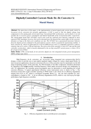
converter efficiency. A typical experimental efficiency versus load-current curve is shown in Fig. 1. The
maximu m current draw of the controller operating in PWM mode is also shown for an efficiency degradation
ranging fro m 0.2% to 2%, which is considered acceptable. Below mA, the total controller cur- rent-
consumption is limited to 250 A for an efficiency degradation of 0.2%, which is very chall en gin g for h igh-
performance, high-frequency controllers.
Fig. 1. Efficiency degradation due to controller power consumption.
46
2. DigitallyControlled Current-Mode Dc–Dc Converter Ic…
Fig. 2. Synchronous buck converter with mixed -signal current mode control.
Below several hundred MHz, full monolithic integration in CM OS processes is not feasible today, due
to size and cost con- straints for the passive components [1]. Instead, the system-in- package (SiP) solutio n is
gaining mo m ent u m for high-efficiency onversion in the several-to-ten’s of MHz range. SiP consists of packaging
the die and passives together to reduce the footprint and parasitics [2]. Several dc–dc converters having in-
package inductors that use proprietary packaging/integration techniques have been intro du c e d [2] –[ 4] . In cludi ng
the inductor in the same package as the die allows further optimizat ion of the efficiency compared to traditional
designs, where the inductor characteristics are unknown to the IC manufacturer. This work is targeted to SiP
applications in the 2–10 MHz range. Peak current-mode control (CPM) provides inherent cycle-by-cycle
current-limiting in the power transistors and simplified loop dynamics, wh ich allows simp le and robust
compensation of the control-loop [5] as shown basic architecture was first reported in [16]. In addition
to providing numerous additional imp lementation details and new measurement results, this paper examines the
effect of charge/discharge current mis match inside the charge- pump on the converter’s closed-loop operation
and reaches new conclusions about the application range of this topology. This paper also investigates the effect
of current source mismatch in the DAC architecture. This paper is organized as follows. The limit-cycle
phenomenon for mixed-signal CPM is analyzed in Sect ion II, leading to minimu m resolution requirements for
the DAC. The pro- posed low-power DAC architecture fo r linking the voltage and current loops is presented in
Section III. The high-bandwidth analog current sensing scheme is presented in Section V and experimental
results for the fabricated prototype are reported in Section VII.
2. Limit-Cycle Oscillations In Current- Mode Control
Unless otherwise stated, it is assumed that the converter runs in CPM without slope-compensation,
which implies that the steady-state duty-cycle is limited to in order to avoid inherent instability in the current
loop [5]. Instability in the un- compensated current loop has been shown to appear slightly
below[17].Thetwoquantizers (the DAC and the ADC) in the feedback loop make hybrid CPM prone to limit-
cycle oscillat ions, a phe- nomenon which is well understood in digital voltage-mode controllers [18], [19]. In this
section, the analysis method presented in [18] is extended for the hybrid CPM. The DC output voltage change
caused by changing the DAC input by one LSB, , is given bydomain, while the current-regulation loop
has a traditional analog imp lementation. Using this architecture, a DAC is required at the interface of the two
loops, in order to generate an analog current command. Mixed-signal CPM benefits from the simplicity of the
analog current loop and the flexib ility of the digitally compensated voltage loop. With this approach, a
reconfigurable digital co mpensator can be used without the need for sampling the inductor current. The high-
frequency digital pulse-width modulator (DPWM) required for fu lly d igital CPM schemes [12]–[14] is also
eliminated, resulting in a practical, low-cost implementation.The design of a low-power DAC specialized for
mix e d-si gn al CPM is the main focus of this work. A flash architecture is not appropriate due to high power
consumption, which limits the light-load efficiency of the buck converter. In [11], a on e- bit DAC was used to
meet the tight resolution re quir e m e nts of mixed-signal CPM; however, the low-pass rec o nstru ctio n filter in
the DAC introduces an undesirable pole in the syste m transfer function. Th is pole limits the control
bandwidth and overall regulation performance. An adaptive control sch e m e was develop ed to address this
issue [11], where the DAC over-samp ling rate and filter corner frequency of the DA C are varied in real-time
to achieve both low steady-state pow e r consumption and fast transient response. In this work, the aim is to
eliminate the main shortcomings of the previous
47
3. DigitallyControlled Current-Mode Dc–Dc Converter Ic…
Fig. 3. Simp lified architecture of the integrated dc–dc converter with a hybrid CPM control scheme and the
novel DAC.
D AC approach, namely the bandwidth restriction imposed by the DAC’s low-pass filter, while at the
same time generating a high resolution voltage reference for the current-loop. The si mpl e low-power DAC
architecture is applied to the hybrid sch e m e for a synchronous buck converter IC, as shown in Fig. 3. The
IC includes the control circu its, as well as a seg m e nt ed power-stage [15] for imp roving light-load
efficiency. Unlik e othe r top olo gies topologies, the proposed DAC does not require ext ensiv e digital signal
processing (noise shaping) or high-fr eq u en c y clocks beyond the switching frequency. The CP-DAC basic
architecture was first reported in [16]. In addit ion to providing numerous additional implementation details
and new measurement results, this paper examines the effect of charge/discharge current mis match inside the
charge- pump on the converter’s closed-loop operation and reaches new conclusions about the application range
of this topology. This paper also investigates the effect of current source mis match in the DAC architecture.This
paper is organized as follows. The limit -cycle phenom- enon for mixed-signal CPM is analyzed in Section II,
leading to minimu m resolution requirements for the DAC. The pro- posed low-power DAC architecture for
lin king the voltage and current loops is presented in Section III. The high-bandwidth analog current sensing
scheme is presented in Section V and experimental results
TABLE I SYSTEM SPECIFICATIONS
48
4. DigitallyControlled Current-Mode Dc–Dc Converter Ic…
Fig.4 . Load-step response showing the effect of dec r ea sing b y 2.5 fro m (a) to (b).
Fig. 5. Min imu m DAC resolution for different values of .
The minimu m resolution is highly load dependent. The resolution requirements in DCM mode are
analyzed in [20]. The presence of limit-cycle oscillations in the inductor current is con- firmed experimentally
in the load-step response of Fig. 6. For a fixed DAC resolution, reducing the sensing gain . The oscillations
in Fig. 4(b) disappear when the voltage loop is opened, proving that the oscillat ions are due to the outer
regulation loop. The result is shown in Fig. 5, for the parameters of Table I. The high control-to-output gain in
CPM results in a higher resolution requirement for the DAC, co mpared to the DPWM in voltage-mode
control. It can be seen that unlike voltage-mode control in continuous-conduction mode (CCM), the min imu m
resolution is highly load dependent. The resolution requirements in DCM mode are analyzed in [20]. The
presence of limit-cycle oscillations in the inductor current is con- firmed experimentally in the load-step
response of Fig. 4. The output voltage versus current command, obtained from solving (6), is shown in Fig.
6(a) for different values of and for the parameters given in Table I. The current-loop gain from (7) is
plotted in Fig. 4(b). In both cases, the duty-cycle limit of is shown by the dashed line, beyond which the
current loop is inherently unstable [5].
49
5. DigitallyControlled Current-Mode Dc–Dc Converter Ic…
Fig. 6. (a) Output voltage versus current-command and (b) small-signal gain fo r d ifferent values
3. CLOSED-LOOP RESPONS E
An accurate system model was generated in Matlab/ Simu lin k, based on the extracted parameters of the
power-stage and the mixed-signal blocks, as well as the fin ite precision of the digital registers in the digital
compensator. The simu lated step-response for the closed-loop system is shown in Fig. 14(a) and (b) for 50–
250 mA and 50–500 mA load steps, respectively. The output voltage is regulated back into the zero-error
bin within about 5 s for a load-step of 50–250 mA. The differential current-command
waveform shows that the CP-DAC immed iately adjusts the peak inductor current following the load-step. The
system parameters are summarized in Table I. As mentioned in Section III, the mismatch in the bi- nary-
weighted sources in the programmab le current sink can lead to a no monotonic characteristic from despite
the fact that is monotonic with respect to the target . Th is effect was investigated by simulat ing
the converter in closed-loop with different comb inations of mismatch in the binary weighted current sinks of
Fig. 6, ranging fro m 0 to 20% of. The ideal ratios were varied fro m. The overlapped CP-DAC input/output
characteristics are shown in Fig. 7(a). The figure also includes the characteristic for an ideal DAC with uniform
quantization. The resulting 29 closed-loop responses are overlapped in Fig. 7(b). The simulat ion confirms that
the response is stable in all cases, with only minor d ifferences in the settling time and voltage fluctuation.
Fig 7 (a) Overlapped CP-DAC input/output characteristic for different co mb inations of the current sink ratios in
the CP-DAC. (b) Overlapped closed-loop
50– 500 mA load-step responses for the 28 comb inations of CP-DAC characteristics, showing the minor effect o f
the CP-DAC nonlinearity.
4. E XP E RI M E N TAL RE S ULT S
The converter shown in Fig. 8 includes a segmented power- stage similar to [29] for improved light-
load efficiency. It was fabricated in a 0.18 m CM OS process with 5 V transistors, which are sufficient to
accommodate the single-cell lithiu m-ion battery voltage range of 2.7 V to 4.2 V. The chip micrograph is shown
in Fig. 17. The die measures10mm, while the total active area for the controller (excluding the power-stage) is
only 0.077 . The total controller current-draw, wh ich is do minated by the on-chip senseFET current-
sensor, is below 250 A at 1 0 mA. The current-draw and active area of each block are given in Tab le II.
50
6. DigitallyControlled Current-Mode Dc–Dc Converter Ic…
Fig. 8. Simu lated closed-loop response with a 15 % mi s m atc h between the charge and discharge currents in
the CP DAC.
Table Ii
Summary Of Area And Po wer Consumption For The Controller
Portion Of The Cp m Ic
5. CON CL USI ON
A low-power solution has been proposed for implement ing mixed-signal peak current-mode control
in dc–dc converters for portable applications. The charge-pump DAC has relatively poor linearity co mpared
to more expensive DAC topologies; however, this can be tolerated since the system runs in closed-loop.
The CP-DAC has a guaranteed monotonic behavior from the digital current co mmand to the peak
inductor current which is essential for maintain ing stability. It was shown that mismatches in the charge
and discharge currents in the charge-pump make it impossible to internal store in the digital do main
without using some form of calibrat ion. This is not a major limitation since many linear and nonlinear
digital co mpensators can be implemented simply by calculating each cycle. A major advantage of the
CP-DAC over flash and architectures is the fact that it consumes nearly zero current when the dc–dc
converter is in steady-state. The power consumption of the CP-DAC scales with the frequency of the load
transients. The prototype IC has a fast transient response which can be further improved by using a more
sophisticated compensator. The operating frequency was primarily limited by the bandwidth of the current
sensor, since the power-stage can easily operate beyond 10 MHz. The output voltage range can easily be
extended by imp lementing tradit ional analog slope co mpensation.
Authors
M. Murali has obtained his B.E. (Electrical and Electronics Engineering) fro m Anna University, Chennai in
2010. He is comp leted his M.Tech. (Power Electron ics) fro m JNTU Anantapur. He is editor of International
journal of Emerging Technology and Advanced Engineering. His research area of interest includes Power
Electronics and Embedded Systems.
P.Sundra moorthy has obtained his B.E. &M.E degree fro m Anna University, Chennai Respectively.
Currently doing his research scholar fro m periyar maniammai university. He has 6 years of teaching
experience. His research area of interest includes Power Electronics and Instrumentation.
M.Karthik has obtained his B.Tech.(Electrical and Electronics Engineering) fro m JNTUA Un iversity,
Ananthapur in 2009. He is currently pursuing his M.Tech. (Power Electronics) fro m JNTU Anantapur. His
research area of interest includes Power Electronics and Po wer Systems.
51
7. DigitallyControlled Current-Mode Dc–Dc Converter Ic…
References
[1] M. Alimadadi, S. Sheikhaei, G. Lemieux, S. Mirabbasi, and P. Palmer, “A 3 GHz switching DC–DC converter using clock-tree
charge recy- cling in 90 nm CMOS with integrated output filter,” in Proc. IEEE Int. Solid-State Circuits Conf., 2007, pp. 532–533.
[2] Z. Hayashi, Y. Katayama, M. Edo, and H. Nishio, “High efficiency dc–dc converter chip size modul e with integrated soft
ferrite,” IEEE Trans. Magn., vol. 39, no. 5, pp. 3068–3072, Sep. 2003.
[3] MIC3385: 8 mhz Inductorless Buck Regulator With LDO Standby
Mode Datasheet, micrel, 2007 [Online]. Available: http://www.mi- crel.com
[4] Ep53 52q/ ep5 362q/ ep 5382 q -5 00/6 00/80 0 ma Synchronous Buck Reg- ulators With Integrated Inductor Datasheet, Enpirion, 2006
[Online]. Available: http://www.enpirion.com
[5] R. Erickson and D. Maksimovic, Fundamentals of Power Elec- tronics. Norwell, MA: Kluwer, 2001.
´
[6] C. Lee and P. Mok, “A monolithic current-mode CMOS DC–DC
converter with on-chip current-sensing technique,” IEEE J. Solid-State
Circuits, vol. 39, no. 1, pp. 3–14, 2004.
[7] H. Forghani-Zadeh and G. Rincon-Mora, “An accurate, continuous, and lossless self-learning CMOS current-sensing scheme for
inductor- based DC–DC converters,” IEEE J. Solid-State Circuits, vol. 42, no. 3, pp. 665–679, Mar. 2007.
[8] M. Du and H. Lee, “A 2.5 MHz, 97%-accuracy on-chip current sensor with dynamically-biased shunt feedback for current-mode
switching DC–DC converters,” in Proc. IEEE Int. Symp. Circuits Syst., 2008, pp.
3274–3277.
[9] Y. Ahn, H. Nam, and J. Roh, “A 93.5% efficiency, 400-ma current- mode DC–DC buck converter with watchdog functions,” in
Proc. Int.
SoC Design Conf. (ISOCC), Nov. 2009, pp. 428–431.
[10] S. Saggini and M. Ghioni, “An innovative digital control architecture for low-voltage high-current DC–DC converters with tight
load regu-
lation,” IEEE Trans. Power Electron., vol. 19, no. 1, pp. 210–218, Jan.
2004.
[11] O. T rescases, Z. Lukic, W.-T. Ng, and A. Prodic, “ A low power mixed-signal current-mode DC–DC converter using a
´ ´
one-bit delta
sigma DAC,” in Proc. IEEE Applied Power Electron. Conf. Expo.,
2006, pp. 700–704.
[12] H. Peng and D. Maksimovic, “Digital current-mode controller for
´
DC–DC converters,” in Proc. IEEE Applied Power Electron. Conf. Expo., 2005, pp. 899–905.
[13] S. Chattopadhyay and S. Das, “ A digital current-mode control tech-
nique for DC–DC converters,” IEEE Trans. Power Electron., vol. 21, no. 6, pp. 1718–1726, 2006.
[14] Y.-S. Jung, “Small-signal model-based design of digital currrent-mode control,” IEEE Proc. Elect. Power Appl., vol. 152, no. 4, 2005.
[15] R. Williams, W. Grabowski, A. Cowell, M. Darwish, and J.
Berwick, “The dual-gate W-switched power MOSFET: A new concept for improving light load efficiency in DC/DC
converters,”
in Proc. IEEE Int. Symp. Power Se mi con d. Devi ce s ICs, 1997,
pp. 193–196.
[16] O. Trescases, N. Rahman, A. Prodic, and W. T. Ng, “ A 1 V buck converter IC with hybrid current-mode control and a
charge-pump
dac,” in IEEE Power Electron. Specialists Conf. (PESC), Jun. 2008, pp. 1122–1128.
[17] R. Ridley,“ A new small-signal model for current-mode control,”Ph.D. dissertation, Virginia Polytechnic Inst., Blacksburg, 1990.
[18] A. Peterchev and S. Sanders, “ Qu anti zatio n resolution and limit cycling in digitally controlled PWM converters,” IEEE Trans. Power
Electron., vol. 18, pp. 301–308, Jan. 2003.
[19] H. Peng, A. Prodic, E. Alarcon, and D. Maksimovic, “Modeling of quantization effects in digitally cont roll ed DC–DC
´ ´
converters,” IEEE
Trans. Power Electron., vol. 22, no. 1, pp. 208–209, 2007.
[20] J. Chen, M. Ribeiro, R. Payseo, D. Zhou, and J. Smith, “DPWM
time resolution requirements for digitally controlled DC–DC con- verters,” in Proc. IEEE Applied Power Electron. Conf.
Expo., 2006, pp. 1127–1132.
52
![DigitallyControlled Current-Mode Dc–Dc Converter Ic…
Fig. 2. Synchronous buck converter with mixed -signal current mode control.
Below several hundred MHz, full monolithic integration in CM OS processes is not feasible today, due
to size and cost con- straints for the passive components [1]. Instead, the system-in- package (SiP) solutio n is
gaining mo m ent u m for high-efficiency onversion in the several-to-ten’s of MHz range. SiP consists of packaging
the die and passives together to reduce the footprint and parasitics [2]. Several dc–dc converters having in-
package inductors that use proprietary packaging/integration techniques have been intro du c e d [2] –[ 4] . In cludi ng
the inductor in the same package as the die allows further optimizat ion of the efficiency compared to traditional
designs, where the inductor characteristics are unknown to the IC manufacturer. This work is targeted to SiP
applications in the 2–10 MHz range. Peak current-mode control (CPM) provides inherent cycle-by-cycle
current-limiting in the power transistors and simplified loop dynamics, wh ich allows simp le and robust
compensation of the control-loop [5] as shown basic architecture was first reported in [16]. In addition
to providing numerous additional imp lementation details and new measurement results, this paper examines the
effect of charge/discharge current mis match inside the charge- pump on the converter’s closed-loop operation
and reaches new conclusions about the application range of this topology. This paper also investigates the effect
of current source mismatch in the DAC architecture. This paper is organized as follows. The limit-cycle
phenomenon for mixed-signal CPM is analyzed in Sect ion II, leading to minimu m resolution requirements for
the DAC. The pro- posed low-power DAC architecture fo r linking the voltage and current loops is presented in
Section III. The high-bandwidth analog current sensing scheme is presented in Section V and experimental
results for the fabricated prototype are reported in Section VII.
2. Limit-Cycle Oscillations In Current- Mode Control
Unless otherwise stated, it is assumed that the converter runs in CPM without slope-compensation,
which implies that the steady-state duty-cycle is limited to in order to avoid inherent instability in the current
loop [5]. Instability in the un- compensated current loop has been shown to appear slightly
below[17].Thetwoquantizers (the DAC and the ADC) in the feedback loop make hybrid CPM prone to limit-
cycle oscillat ions, a phe- nomenon which is well understood in digital voltage-mode controllers [18], [19]. In this
section, the analysis method presented in [18] is extended for the hybrid CPM. The DC output voltage change
caused by changing the DAC input by one LSB, , is given bydomain, while the current-regulation loop
has a traditional analog imp lementation. Using this architecture, a DAC is required at the interface of the two
loops, in order to generate an analog current command. Mixed-signal CPM benefits from the simplicity of the
analog current loop and the flexib ility of the digitally compensated voltage loop. With this approach, a
reconfigurable digital co mpensator can be used without the need for sampling the inductor current. The high-
frequency digital pulse-width modulator (DPWM) required for fu lly d igital CPM schemes [12]–[14] is also
eliminated, resulting in a practical, low-cost implementation.The design of a low-power DAC specialized for
mix e d-si gn al CPM is the main focus of this work. A flash architecture is not appropriate due to high power
consumption, which limits the light-load efficiency of the buck converter. In [11], a on e- bit DAC was used to
meet the tight resolution re quir e m e nts of mixed-signal CPM; however, the low-pass rec o nstru ctio n filter in
the DAC introduces an undesirable pole in the syste m transfer function. Th is pole limits the control
bandwidth and overall regulation performance. An adaptive control sch e m e was develop ed to address this
issue [11], where the DAC over-samp ling rate and filter corner frequency of the DA C are varied in real-time
to achieve both low steady-state pow e r consumption and fast transient response. In this work, the aim is to
eliminate the main shortcomings of the previous
47](data:image/gif;base64,R0lGODlhAQABAIAAAAAAAP///yH5BAEAAAAALAAAAAABAAEAAAIBRAA7)