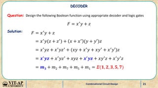
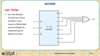
This document discusses combinational circuit design and decoders. It contains:
- An overview of binary adders, decoders, encoders, multiplexers and other combinational circuits.
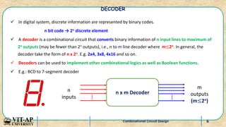
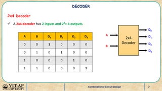
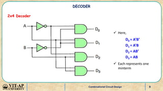
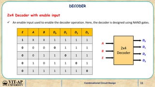
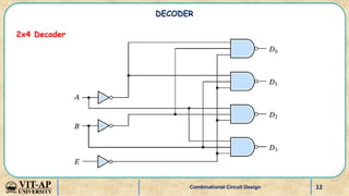
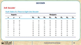
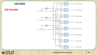
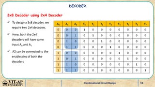
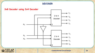
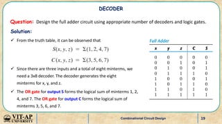
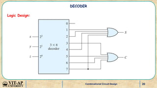
- Explanations and truth tables for 2x4 and 3x8 decoders. Decoders are used to convert binary codes to discrete outputs.
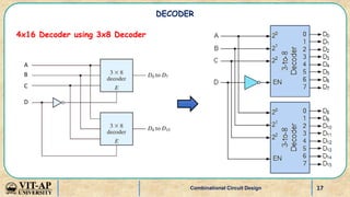
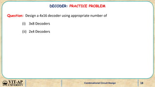
- Examples of designing higher order decoders using lower order decoders, and implementing Boolean functions with decoders.