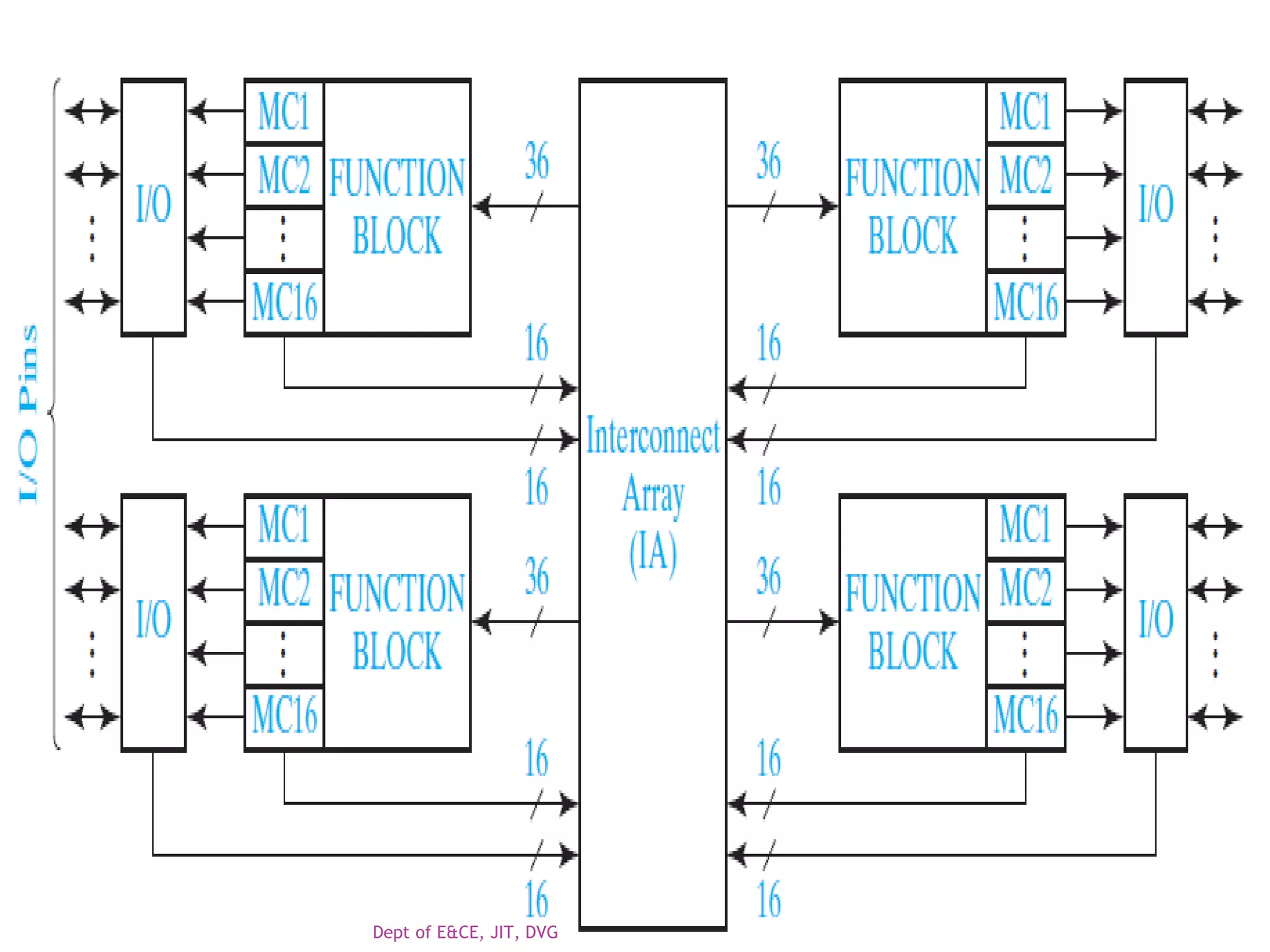
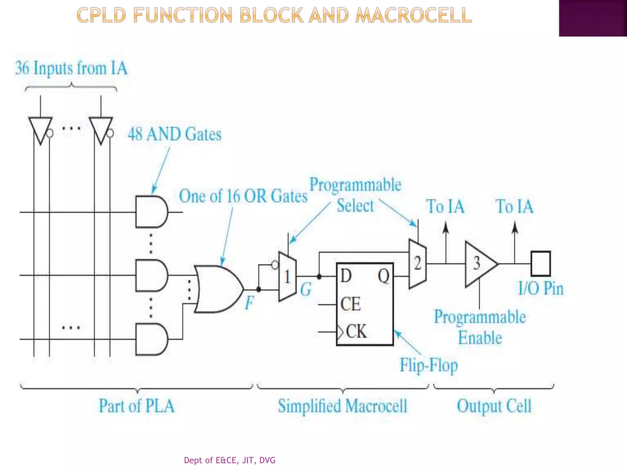
Dept of E&CE, JIT, DVG
 As integrated circuit technology continues to
improve, more and more gates can be placed on a
single chip
 Instead of a single PAL or PLA on a chip, many PALs
or PLAs can be placed on a single CPLD chip and
interconnected.
 When storage elements such as flip-flops are also
included on the same IC, a small digital system can
be implemented with a single CPLD.
 Figure shows the basic architecture Xilinx
XCR3064XL CPLD
Dept of E&CE, JIT, DVG
 Has four function blocks,
 Each block has 16 associated macrocells (MC1,MC2, .)
 Each function block is a programmable AND-OR array
that is configured as a PLA.
 Each macrocell contains a flip-flop and multiplexers
that route signals from the function block to the
input-output (I/O) block or to the interconnect array
(IA).
 The IA selects signals from the macrocell outputs or
I/O blocks and connects them back to function block
inputs.
 Thus, a signal generated in one function block can be
used as an input to any other function block.
 The I/O blocks provide an interface between the bi-
directional I/O pins on the IC and the interior of the
CPLD
Dept of E&CE, JIT, DVG
 Figure shows how a signal generated in the PLA is
routed to an I/O pin through a macrocell.
 Any of the 36 outputs from the IA (or their
complements) can be connected to any inputs of
the 48 AND gates.
 Each OR gate can accept up to 48 product term
inputs from the AND array.
 The first MUX (1) can be programmed to select the
OR-gate output or its complement.
 The MUX (2) at the output of the macrocell can be
programmed to select either the combinational
output (G) or the flip-flop output (Q).
 This output goes to the interconnect array and to
the output cell.
Dept of E&CE, JIT, DVG
 The output cell includes a three-state buffer (3) to
drive the I/O pin.
 When the I/O pin is used as an input, the buffer
must be disabled
Dept of E&CE, JIT, DVG
 An FPGA is an IC that contains an array of identical
logic cells with programmable interconnections.
 The user can program the functions realized by
each logic cell and the connections between the
cells.
 Figure shows the layout of part of a typical FPGA.
 The interior of the FPGA consists of an array of
logic cells, also called configurable logic blocks
(CLBs).
 The array of CLBs is surrounded by a ring of input-
output interface blocks.
 These I/O blocks connect the CLB signals to IC pins.
 The space between the CLBs is used to route
connections between the CLB outputs and inputs.
Dept of E&CE, JIT, DVG
 This CLB contains two function generators, two flip-flops,
and various multiplexers for routing signals within the CLB.
 Each function generator has four inputs and can implement
any function of up
 to four variables. The function generators are implemented
as lookup tables (LUTs).
 A four-input LUT is essentially a reprogrammable ROM with
16 1-bit words. This
 ROM stores the truth table for the function being generated.
The H multiplexer
 selects either F or G depending on the value of H1. The CLB
has two combinational
 outputs (X and Y) and two flip-flop outputs (XQ and YQ).
The X and Y outputs and
Dept of E&CE, JIT, DVG
 To implement a switching function of more than
four variables using 4- variable function
generators, the function must be decomposed into
subfunctions.
 One method of decomposition is based on
Shannon’s expansion theorem.
 Expanding a function of the variables a, b, c, and d
about the variable a:
f(a, b, c, d) = a′ f(0, b, c, d) + a f(1, b, c, d)
= a′ f0 + a f1
Dept of E&CE, JIT, DVG
 The 3-variable function
f0 = f(0, b, c, d) is formed by replacing a with 0 in
f(a, b, c, d), and
f1 = f(1, b, c, d) is formed by replacing a with 1 in
f(a, b, c, d).
• The expansion theorem to a 5-variable function
gives
f(a, b, c, d, e) = a′ f(0, b, c, d, e) + a f(1, b, c, d, e)
= a′ f0 + a f1
 This shows that any 5-variable function can be
realized using two 4-variable function generators
and a 2-to-1 MUX
Dept of E&CE, JIT, DVG
 To realize a 6-variable function using 4-variable
function generators,the expansion theorem twice
G(a, b, c, d, e, f ) = a′G(0, b, c, d, e, f ) + a G(1, b, c, d, e, f )
= a′G0 + a G1
G0 = b′G(0, 0, c, d, e, f ) + b G(0, 1, c, d, e, f )
= b′G00 + b G01
G1 = b′G(1, 0, c, d, e, f ) + b G(1, 1, c, d, e, f )
= b′G10 + bG11
 Because G00,G01,G10, and G11 are all 4-variable
functions, we can realize any 6-variable function using
four 4-variable function generators and three 2-to-1
MUXes, as shown in Figure b
 Thus, we can realize any 6-variable function using two
CLBs of the type shown in Figure
G(a, b, c, d, e, f ) = a′b′G00 + a′b G01 + ab′G10 + ab G11
Dept of E&CE, JIT, DVG

CPLD.pptx

  • 1.
    Dept of E&CE,JIT, DVG
  • 2.
     As integratedcircuit technology continues to improve, more and more gates can be placed on a single chip  Instead of a single PAL or PLA on a chip, many PALs or PLAs can be placed on a single CPLD chip and interconnected.  When storage elements such as flip-flops are also included on the same IC, a small digital system can be implemented with a single CPLD.  Figure shows the basic architecture Xilinx XCR3064XL CPLD Dept of E&CE, JIT, DVG
  • 3.
    Dept of E&CE,JIT, DVG
  • 4.
     Has fourfunction blocks,  Each block has 16 associated macrocells (MC1,MC2, .)  Each function block is a programmable AND-OR array that is configured as a PLA.  Each macrocell contains a flip-flop and multiplexers that route signals from the function block to the input-output (I/O) block or to the interconnect array (IA).  The IA selects signals from the macrocell outputs or I/O blocks and connects them back to function block inputs.  Thus, a signal generated in one function block can be used as an input to any other function block.  The I/O blocks provide an interface between the bi- directional I/O pins on the IC and the interior of the CPLD Dept of E&CE, JIT, DVG
  • 5.
    Dept of E&CE,JIT, DVG
  • 6.
     Figure showshow a signal generated in the PLA is routed to an I/O pin through a macrocell.  Any of the 36 outputs from the IA (or their complements) can be connected to any inputs of the 48 AND gates.  Each OR gate can accept up to 48 product term inputs from the AND array.  The first MUX (1) can be programmed to select the OR-gate output or its complement.  The MUX (2) at the output of the macrocell can be programmed to select either the combinational output (G) or the flip-flop output (Q).  This output goes to the interconnect array and to the output cell. Dept of E&CE, JIT, DVG
  • 7.
     The outputcell includes a three-state buffer (3) to drive the I/O pin.  When the I/O pin is used as an input, the buffer must be disabled Dept of E&CE, JIT, DVG
  • 8.
     An FPGAis an IC that contains an array of identical logic cells with programmable interconnections.  The user can program the functions realized by each logic cell and the connections between the cells.  Figure shows the layout of part of a typical FPGA.  The interior of the FPGA consists of an array of logic cells, also called configurable logic blocks (CLBs).  The array of CLBs is surrounded by a ring of input- output interface blocks.  These I/O blocks connect the CLB signals to IC pins.  The space between the CLBs is used to route connections between the CLB outputs and inputs. Dept of E&CE, JIT, DVG
  • 9.
    Dept of E&CE,JIT, DVG
  • 10.
    Dept of E&CE,JIT, DVG
  • 11.
     This CLBcontains two function generators, two flip-flops, and various multiplexers for routing signals within the CLB.  Each function generator has four inputs and can implement any function of up  to four variables. The function generators are implemented as lookup tables (LUTs).  A four-input LUT is essentially a reprogrammable ROM with 16 1-bit words. This  ROM stores the truth table for the function being generated. The H multiplexer  selects either F or G depending on the value of H1. The CLB has two combinational  outputs (X and Y) and two flip-flop outputs (XQ and YQ). The X and Y outputs and Dept of E&CE, JIT, DVG
  • 12.
     To implementa switching function of more than four variables using 4- variable function generators, the function must be decomposed into subfunctions.  One method of decomposition is based on Shannon’s expansion theorem.  Expanding a function of the variables a, b, c, and d about the variable a: f(a, b, c, d) = a′ f(0, b, c, d) + a f(1, b, c, d) = a′ f0 + a f1 Dept of E&CE, JIT, DVG
  • 13.
     The 3-variablefunction f0 = f(0, b, c, d) is formed by replacing a with 0 in f(a, b, c, d), and f1 = f(1, b, c, d) is formed by replacing a with 1 in f(a, b, c, d). • The expansion theorem to a 5-variable function gives f(a, b, c, d, e) = a′ f(0, b, c, d, e) + a f(1, b, c, d, e) = a′ f0 + a f1  This shows that any 5-variable function can be realized using two 4-variable function generators and a 2-to-1 MUX Dept of E&CE, JIT, DVG
  • 14.
    Dept of E&CE,JIT, DVG
  • 15.
     To realizea 6-variable function using 4-variable function generators,the expansion theorem twice G(a, b, c, d, e, f ) = a′G(0, b, c, d, e, f ) + a G(1, b, c, d, e, f ) = a′G0 + a G1 G0 = b′G(0, 0, c, d, e, f ) + b G(0, 1, c, d, e, f ) = b′G00 + b G01 G1 = b′G(1, 0, c, d, e, f ) + b G(1, 1, c, d, e, f ) = b′G10 + bG11  Because G00,G01,G10, and G11 are all 4-variable functions, we can realize any 6-variable function using four 4-variable function generators and three 2-to-1 MUXes, as shown in Figure b  Thus, we can realize any 6-variable function using two CLBs of the type shown in Figure G(a, b, c, d, e, f ) = a′b′G00 + a′b G01 + ab′G10 + ab G11 Dept of E&CE, JIT, DVG
  • 16.
    Dept of E&CE,JIT, DVG