5 unit.pdf vlsi unit 2 important notes for ece department
1. UNIT V: IMPLEMENTATION STRATEGIES AND TESTING
IMPLEMENTATION STRATEGIES
1. FPGA building block architectures
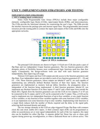
Xilinx Field Programmable Gate Arrays (FPGAs) include three major configurable
elements: configurable logic blocks (CLBs), input/output blocks (IOBs), and interconnections.
The CLBs provide the functional elements for constructing the user’s logic. The IOBs provide
the interface between the package pins and internal signal lines. The programmable interconnect
resources provide routing paths to connect the inputs and outputs of the CLBs and IOBs onto the
appropriate networks.
Figure 1.8 FPGA Architecture
The principal CLB elements are shown in Figure 1.8 Each new CLB also packs a pair of
flip-flops and two independent 4-input function generators. The two function generators offer
designers plenty of flexibility because most combinatorial logic functions need less than four
inputs. Consequently, the design-software tools can deal with each function generator
independently, thus improving cell usage.
Thirteen CLB inputs and four CLB outputs provide access to the function generators and
flip-flops. Four independent inputs are provided to each of two function generators (F1 – F4 and
G1 – G4). These function generators, whose outputs are labeled F' and G', are each capable of
implementing any arbitrarily defined Boolean function of their four inputs. The function
generators are implemented as memory look-up tables; therefore, the propagation delay is
independent of the function being implemented. A third function generator, labeled H', can
implement any Boolean function of its three inputs: F' and G' and a third input from outside the
block (H1). Signals from the function generators can exit the CLB on two outputs; F' or H' can
be connected to the X output, and G' or H' can be connected to the Y output. Thus, a CLB can be
used to implement any two independent functions of up-to-four variables, or any single function
of five variables, or any function of four variables together with some functions of five variables,
or it can implement even some functions of up to nine variables. Implementing wide functions in
a single block reduces both the number of blocks required and the delay in the signal path,
achieving both increased density and speed.
The two storage elements in the CLB are edge-triggered D-type flip-flops with common
clock (K) and clock enable (EC) inputs. A third common input (S/R) can be programmed as
either an asynchronous set or reset signal independently for each of the two registers; this input
also can be disabled for either flip-flop. A separate global Set/ Reset line sets or clears each
register during power-up, reconfiguration, or when a dedicated Reset net is driven active. This
2. Reset net does not compete with other routing resources; it can be connected to any package pin
as a global reset input.
Figure 1.9. Configurable Logic Block
Each flip-flop can be triggered on either the rising or falling clock edge. The source of a
flip-flop data input is programmable: it is driven either by the functions F', G', and H', or the
Direct In (DIN) block input. The flip-flops drive the XQ and YQ CLB outputs. In addition, each
CLB F' and G' function generator contains dedicated arithmetic logic for the fast generation of
carry and borrow signals, greatly increasing the efficiency and performance of adders,
subtracters, accumulators, comparators and even counters.
Multiplexers in the CLB map the four control inputs, labeled C1 through C4 in Figure
1.9, into the four internal control signals (H1, DIN, S/R, and EC) in any arbitrary manner.
The flexibility and symmetry of the CLB architecture facilitates the placement and
routing of a given application. Since the function generators and flip-flops have independent
inputs and outputs, each can be treated as a separate entity during placement to achieve high
packing density. Inputs, outputs, and the functions themselves can freely swap positions within a
CLB to avoid routing congestion during the placement and routing operation.
Input/Output Blocks (IOBs
User-configurable IOBs provide the interface between external package pins and the
internal logic (Figure 3). Each IOB controls one package pin and can be defined for input,
output, or bidirectional signals. Two paths, labeled I1 and I2, bring input signals into the array.
Inputs are routed to an input register that can be programmed as either an edge-triggered flip-flop
or a level-sensitive transparent latch. Optionally, the data input to the register can be delayed by
several nanoseconds to compensate for the delay on the clock signal that first must pass through
a global buffer before arriving at the IOB. This eliminates the possibility of a data hold-time
requirement at the external pin. The I1 and I2 signals that exit the block can each carry either the
direct or registered input signal. Output signals can be inverted or not inverted, and can pass
directly to the pad or be stored in an edge-triggered flip-flop. Optionally, an output enable signal
can be used to place the output buffer in a high-impedance state, implementing 3-state outputs or
bidirectional I/O. Under configuration control, the output (OUT) and output enable (OE) signals
can be inverted, and the slew rate of the output buffer can be reduced to minimize power bus
transients when switching non-critical signals.
3. Figure 1.10 Input / Output Block
There are a number of other programmable options in the IOB. Programmable pull-up
and pull-down resistors are useful for tying unused pins to VCC or ground to minimize power
consumption. Separate clock signals are provided for the input and output registers; these clocks
can be inverted, generating either falling-edge or rising-edge triggered flip-flops. Embedded
logic attached to the IOBs contains test structures compatible with IEEE Standard 1149.1 for
boundary scan testing, permitting easy chip and board-level testing.
Programmable Interconnect
All internal connections are composed of metal segments with programmable switching
points to implement the desired routing. An abundance of different routing resources is provided
to achieve efficient automated routing. The number of routing channels is scaled to the size of
the array; i.e., it increases with array size.
There are three main types of interconnect, distinguished by the relative length of their
segments: single-length lines, double-length lines, and Longlines. The routing scheme was
designed for minimum resistance and capacitance of the average routing path, resulting in
significant performance improvements.
The single-length lines are a grid of horizontal and vertical lines that intersect at a Switch Matrix
between each block. Figure 4 illustrates the single-length interconnect lines surrounding one
CLB in the array.
Figure 1.11 Typical CLB Connections to Adjacent Single-Length Lines
4. Each Switch Matrix consists of programmable n-channel pass transistors used to
establish connections between the single-length lines (Figure 1.11). For example, a signal
entering on the right side of the Switch Matrix can be routed to a single-length line on the top,
left, or bottom sides, or any combination thereof, if multiple branches are required. Single-length
lines are normally used to conduct signals within a localized area and to provide the branching
for nets with fanout greater than one.
Figure 1.12 Switch Matrix
Figure 1.13 Double-Length Lines
The double-length lines (Figure 1.13) consist of a grid of metal segments twice as long
as the single-length lines; i.e, a double-length line runs past two CLBs before entering a Switch
Matrix. Double-length lines are grouped in pairs with the Switch Matrices staggered so that each
line goes through a Switch Matrix at every other CLB location in that row or column. As with
single-length lines, all the CLB inputs except K can be driven from any adjacent double length
line, and each CLB output can drive nearby double length lines in both the vertical and
horizontal planes. Double-length lines provide the most efficient implementation of intermediate
length, point-to-point interconnections.
Longlines form a grid of metal interconnect segments that run the entire length or width
of the array (Figure 1.14). Additional vertical longlines can be driven by special global buffers,
designed to distribute clocks and other high fanout control signals throughout the array with
minimal skew. Longlines are intended for high fan-out, time-critical signal nets. Each Longline
has a programmable splitter switch at its center, that can separate the line into two independent
routing channels, each running half the width or height of the array. CLB inputs can be driven
from a subset of the adjacent Longlines; CLB outputs are routed to the Longlines via 3-state
buffers or the single-length interconnected lines.
Figure 1.14 Longline Routing Resources with Typical CLB Connections
Communication between Longlines and single-length lines is controlled by
programmable interconnect points at the line intersections. Double-length lines do not connect to
other lines.
5. 2. FPGA interconnect routing procedures
Classification:
• Global routing
• Detailed routing
• Special Routing
Global Routing
The details of global routing differ slightly between cell-based ASICs, gate arrays, and FPGAs,
but the principles are the same in each case. A global router does not make any connections, it
just plans them. We typically global route the whole chip (or large pieces if it is a large chip)
before detail routing the whole chip (or the pieces). There are two types of areas to global route:
inside the flexible blocks and between blocks.
Goals and Objectives
The input to the global router is a floorplan that includes the locations of all the fixed and
flexible blocks; the placement information for flexible blocks; and the locations of all the logic
cells. The goal of global routing is to provide complete instructions to the detailed router on
where to route every net.
The objectives of global routing are one or more of thefollowing:
Minimize the total interconnect length.
Maximize the probability that the detailed router can complete the routing.
Minimize the critical path delay.
Global Routing Methods
Global routing cannot use the interconnect-length approximations, such as the half-perimeter
measure, that were used in placement. What is needed now is the actual path and not an
approximation to the path length. However, many of the methods used in global routing are still
based on the solutions to the tree on a graph problem.
Sequential routing:
One approach to global routing takes each net in turn and calculates the shortest path using tree
on graph algorithms—with the added restriction of using the available channels. This process is
known as sequential routing. It handle nets one at a time.
Order-dependent and order-independent algorithms:
Using order-independent routing, a global router proceeds by routing each net, ignoring
how crowded the channels are. Whether a particular net is processed first or last does not
matter, the channel assignment will be the same.
In order-independent routing, after all the interconnects are assigned to channels, the
global router returns to those channels that are the most crowded and reassigns some
interconnects to other, less crowded, channels.
Alternatively, a global router can consider the number of interconnects already placed in
various channels as it proceeds. In this case the global routing is order dependent —the
routing is still sequential, but now the order of processing the nets will affect the results.
Hierarchical routing:
Hierarchical routing handles all nets at a particular level at once.
Rather than handling all of the nets on the chip at the same time, the global-routing
6. problem is made more tractable by dividing the chip area into levels of hierarchy.
By considering only one level of hierarchy at a time the size of the problem is reduced at
each level.
There are two ways to traverse the levels of hierarchy.
Starting at the whole chip, or highest level, and proceeding down to the logic cells is the
top-down approach.
The bottom-up approach starts at the lowest level of hierarchy and globally routes the
smallest areas first.
Global Routing Between Blocks
Figure 1.15 illustrates the global-routing problem for a cell-based ASIC. Each edge in the
channel-intersection graph in Figure 1.15 (c) represents a channel. The global router is restricted
to using these channels. The weight of each edge in the graph corresponds to the length of the
channel. The global router plans a path for each interconnect using this graph.
FIGURE 1.15 Global routing for a cell-based ASIC formulated as a graph problem. (a) A cell-
based ASIC with numbered channels. (b) The channels form the edges of a graph. (c) The
channel-intersection graph. Each channel corresponds to an edge on a graph whose weight
corresponds to the channel length.
Figure 1.15 shows an example of global routing for a net with five terminals, labeled A1
through F1, for the cell-based ASIC shown in Figure 1.15 . If a designer wishes to use minimum
total interconnect path length as an objective, the global router finds the minimum-length tree
shown in Figure 1.15 (b). This tree determines the channels the interconnects will use. For
example, the shortest connection from A1 to B1 uses channels 2, 1, and 5 (in that order). This is
the information the global router passes to the detailed router. Figure 1.15 (c) shows that
minimizing the total path length may not correspond to minimizing the path delay between two
points.
FIGURE 1.16 Finding paths in global routing. (a) A cell-based ASIC (from Figure 1.15 )
showing a single net with a fanout of four (five terminals). We have to order the numbered
channels to complete the interconnect path for terminals A1 through F1. (b) The terminals are
7. projected to the center of the nearest channel, forming a graph. A minimum-length tree for the
net that uses the channels and takes into account the channel capacities. (c) The minimum-length
tree does not necessarily correspond to minimum delay. If we wish to minimize the delay from
terminal A1 to D1, a different tree might be better.
Global Routing Inside Flexible Blocks
We shall illustrate global routing using a gate array. Figure 1.16 (a) shows the routing resources
on a sea-of-gates or channelless gate array. The gate array base cells are arranged in 36 blocks,
each block containing an array of 8-by-16 gate-array base cells, making a total of 4068 base
cells.
The horizontal interconnect resources are the routing channels that are formed from unused rows
of the gate-array base cells, as shown in Figure 1.16 (b) and (c). The vertical resources are
feedthroughs. For example, the logic cell shown in Figure 1.16 (d) is an inverter that contains
two types of feedthrough. The inverter logic cell uses a single gate-array base cell with terminals
(or connectors ) located at the top and bottom of the logic cell. The inverter input pin has two
electrically equivalent terminals that the global router can use as a feedthrough. The output of the
inverter is connected to only one terminal. The remaining vertical track is unused by the inverter
logic cell, so this track forms an uncommitted feedthrough.
Feedthrough
A feedthrough is a conductor used to carry a signal through an enclosure or printed
circuit board. Like any conductor, it has a small amount of capacitance. A "feedthrough
capacitor" has a guaranteed minimum value of shunt capacitance built in it and is used for bypass
purposes in ultra-high-frequency applications.[1]
Feedthroughs can be divided into power and
instrumentation categories. Power feedthroughs are used to carry either high current or high
voltage. Instrumentation feedthroughs are used to carry electrical signals (including
thermocouples) which are normally low current or voltage. Another special type is what is
commonly known as RF-feedthrough, specifically designed to carry very high frequency RF or
microwave electrical signals.
A feedthrough electrical connection may have to withstand considerable pressure
difference across its length. Systems that operate under high vacuum, such as electron
microscopes, require electrical connections through the pressure vessel. Similarly, submersible
vehicles require feedthrough connections between exterior instruments and devices and the
controls within the vehicle pressure hull. A very common example of a feedthrough connection
is an automobile spark plug where the body of the plug must resist the pressure and temperature
produced in the engine, while providing a reliable electrical connection to the spark gap in the
combustion chamber. (Spark plugs are occasionally used as low-cost or improvised feedthrough
connections in non-engine applications.)
Detailed Routing
The global routing step determines the channels to be used for each interconnect. Using this
information the detailed router decides the exact location and layers for each interconnect.
Goals and Objectives
The goal of detailed routing is to complete all the connections between logic cells. The most
common objective is to minimize one or more of the following:
The total interconnect length and area
The number of layer changes that the connections have to make
The delay of criticalpaths
Minimizing the number of layer changes corresponds to minimizing the number of vias that
add parasitic resistance and capacitance to a connection. In some cases the detailed router may
8. not be able to complete the routing in the area provided. In the case of a cell-based ASIC or sea-
of-gates array, it is possible to increase the channel size and try the routing steps again. A
channeled gate array or FPGA has fixed routing resources and in these cases we must start all
over again with floorplanning and placement, or use a larger chip.
Typical metal rules:
Figure 1.17 (a) shows typical metal rules. These rules determine the m1 routing pitch
(track pitch, track spacing, or just pitch). We can set the m1 pitch to one of three values:
via-to-via ( VTV ) pitch (or spacing),
via-to-line ( VTL or line-to-via ) pitch, or
line-to-line ( LTL ) pitch.
The same choices apply to the m2 and other metal layers if they are present. Via-to-via spacing
allows the router to place vias adjacent to each other. Via-to-line spacing is hard to use in
practice because it restricts the router to nonadjacent vias. Using line-to-line spacing prevents the
router from placing a via at all without using jogs and is rarely used. Via-to-via spacing is the
easiest for a router to use and the most common. Using either via-to-line or via-to-via spacing
means that the routing pitch is larger than the minimum metal pitch.
In a stacked via the contact cuts all overlap in a layout plot and it is impossible to tell just how
many vias on which layers are present. Figure 1.18 (b–f) show an alternative way to draw
contacts and vias. Though this is not a standard, using the diagonal box convention makes it
possible to recognize stacked vias and contacts on a layout (in any orientation). I shall use these
conventions when it is necessary.
9. Manhattan routing:
In a two-level metal CMOS ASIC technology we complete the wiring using the two different
metal layers for the horizontal and vertical directions, one layer for each direction. This is
Manhattan routing, because the results look similar to the rectangular north–south and east–
west layout of streets in New York City. Thus, for example, if terminals are on the m2 layer, then
we route the horizontal branches in a channel using m2 and the vertical trunks using m1.
In Detailed routing, The routing regions are divided into channels and switchboxes.
So only need to consider the channel routing problem and the switchbox routing problem.
Special Routing
The routing of nets that require special attention, clock and power nets for example, is
normally done before detailed routing of signal nets. The architecture and structure of these nets
is performed as part of floorplanning, but the sizing and topology of these nets is finalized as part
of the routing step.
(i). Clock Routing
Gate arrays normally use a clock spine (a regular grid), eliminating the need for special
routing (Clock Planning‖ ). The clock distribution grid is designed at the same time as the gate-
array base to ensure a minimum clock skew and minimum clock latency—given power
dissipation and clock buffer area limitations. Cell-based ASICs may use either a clock spine, a
clock tree, or a hybrid approach.
FIGURE 1.19 Clock routing.
Figure 1.19 shows how a clock router may minimize clock skew in a clock spine by making the
path lengths, and thus net delays, to every leaf node equal—using jogs in the interconnect paths if
necessary.
More sophisticated clock routers perform
clock-tree synthesis (automatically choosing the depth and structure of the clock tree)
10. clock-buffer insertion (equalizing the delay to the leaf nodes by balancing interconnect
delays and buffer delays).
Clock skew:
In a synchronous circuit clock skew is the difference in the arrival time between two
sequentially-adjacent registers.
In a synchronous circuit, two registers, or flip-flops, are said to be "sequentially adjacent" if
a logic path connects them.
Given two sequentially-adjacent registers Ri and Rj with clock arrival times at destination
and source register clock pins equal to TCi and TCj respectively, clock skew can be
defined as: Tskew i, j = TCi − TCj.
Clock latency:
Clock latency is defined as the amount of time taken by the clock signal in traveling
from its source to the sinks. Clock latency comprises of two components:
Source latency: It is the time taken by the clock signal in traversing from clock source
(may be PLL, oscillator or some other source) to the clock definition point. It is also
known as source insertion delay. It can be used to model off-chip clock latency when
clock source is not part of the chip itself.
Network latency: It is the time taken by the clock signal in traversing from clock
definition point to the sinks of the clock.
Total clock latency at a point, then, is given as follows:
Clock latency = Source latency + Network latency
The clock tree:
The clock tree may contain multiple-driven nodes (more than one active element driving a net).
The net delay models that we have used break down in this case and we may have to extract the
clock network and perform circuit simulation
Another factor contributing to unpredictable clock skew is changes in clock-buffer delays with
variations in power-supply voltage due to data-dependent activity. This activity-induced clock
skew can easily be larger than the skew achievable using a clock router.
The power buses:
The power buses supplying the buffers driving the clock spine carry direct current
(unidirectional current or DC), but the clock spine itself carries alternating current (bidirectional
current or AC). The difference between electromigration failure rates due to AC and DC leads to
different rules for sizing clock buses.
(ii). Power Routing
Each of the power buses has to be sized according to the current it will carry.
Too much current in a power bus can lead to a failure through a mechanism known as
electromigration.
The required power-bus widths can be estimated automatically from library information,
from a separate power simulation tool, or by entering the power-bus widths to the
routing software by hand.
Many routers use a default power-bus width so that it is quite easy to complete routing of
an ASIC without even knowing about this problem.
MTTF for DC current:
For a direct current (DC) the mean time to failure (MTTF) due to electromigration is
experimentally found to obey the following equation:
MTTF = A J –2
exp – E / k T
where J is the current density;
11. E is approximately 0.5 eV;
k is Boltzmann’s constant = 8.62 x 10 –5
eVK–1
;
T is absolute temperature in kelvins.
MTTF for AC current:
There are a number of different approaches to model the effect of an AC component. A typical
expression is
A J –2
exp – E / k T
MTTF = –––––––––––––––––––––––––
J | J | + k AC/DC | J | 2
where J is the average of J(t) , and | J | is the average of | J |. The constant k AC/DC relates the
relative effects of AC and DC and is typically between 0.01 and 0.0001. Electromigration
problems become serious with a MTTF of less than 10 5
hours (approximately 10 years) for
current densities (DC) greater than 0.5 GAm –2
at temperatures above 150 °C.
TABLE 1: Metallization reliability rules for a typical 0.5 micron ( l = 0.25 m m) CMOS
process.
Layer/contact/via Current limit Metal thickness Resistance
m1 1 mA m m –1
7000 Å 95 m W /square
m2 1 mA m m –1
7000 Å 95 m W /square
m3
0.8 m m square m1 contact to diffusion
0.8 m m square m1 contact to poly
0.8 m m square m1/m2 via (via1)
0.8 m m square m2/m3 via (via2)
2 mA m m –1
0.7 mA
0.7 mA
0.7 mA
0.7 mA
12,000 Å 48 m W /square
11 W
16 W
3.6 W
3.6 W
Table 1 lists example metallization reliability rules —limits for the current you can pass through
a metal layer, contact, or via—for the typical 0.5 m m three-level metal CMOS process, G5. The
limit of 1 mA of current per square micron of metal cross section is a good rule-of- thumb to
follow for current density in aluminum-based interconnect.
Power Grid:
Gate arrays normally use a regular power grid as part of the gate-array base.
The gate-array logic cells contain two fixed-width power buses inside the cell, running
horizontally on m1.
The horizontal m1 power buses are then strapped in a vertical direction by m2 buses, which
run vertically across the chip.
The resistance of the power grid is extracted and simulated with SPICE during the base-array
design to model the effects of IR drops under worst-case conditions.
End-Cap Cells:
Standard cells are constructed in a similar fashion to gate-array cells, with power buses
running horizontally in m1 at the top and bottom of each cell.
A row of standard cells uses end-cap cells that connect to the VDD and VSS power buses
placed by the power router.
12. Power routing of cell-based ASICs may include the option to include vertical m2 straps at a
specified intervals. Alternatively the number of standard cells that can be placed in a row
may be limited during placement.
Flip And Abut Technique:
Using three or more layers of metal for routing, it is possible to eliminate some of the
channels completely.
In these cases we complete all the routing in m2 and m3 on top of the logic cells using
connectors placed in the center of the cells on m1.
If we can eliminate the channels between cell rows, we can flip rows about a horizontal axis
and abut adjacent rows together (a technique known as flip and abut)
Routing Summary:
13. TESTING
Introduction:
Testing Verification
Verifies correctness of hardware.
Three main Categories:
– Logic Verification
– Silicon Debug
– Manufacturing Test
Post-silicon process
Verifies correctness of design unit.
Performed by simulation, hardware
emulation or formal methods.
Performed ―once‖ prior to
manufacturing.
Pre-silicon process
Need for Testing:
• To improve the yield
• Yield of a particular IC = the number of good die divided by the total number of die per
wafer.
Testing Levels:
Testing a die (chip) can occur at the following levels:
Wafer level
Packaged chip level
Board level
System level
Field level
Logic Verification:
Verify that the chip performs its intended function
Example: To check whether Adder adds? Counter counts? FSM yield the right outputs at
each cycle? Modem decodes data correctly?
Run before tapeout to verify the functionality
Tapeout is the final result of the design cycle for integrated circuits or printed circuit
boards, the point at which the artwork for the photomask of a circuit is sent for
manufacture.
Silicon Debug:
Run on the first batch of chips that return from fabrication
Confirm that the chip operates as it was intended and help debug any discrepancies.
Require creative detective work to locate the cause of failures
Manufacturing Test
• Verify every transistor, gate and storage element in the chip functions correctly.
• Conducted on each manufactured chip before shipping to the customer to verify that the
silicon is completely intact.
The need to do this arises from a number of manufacturing defects that might occur during either
chip fabrication or accelerated life testing (where the chip is stressed by over-voltage and over-
temperature operation). Typical defects include the following:
Layer-to-layer shorts (e.g., metal-to-metal)
Discontinuous wires (e.g., metal thins when crossing vertical topology jumps)
Missing or damaged vias
Shorts through the thin gate oxide to the substrate or well
These in turn lead to particular circuit a serious problem, including the following:
Nodes shorted to power or ground
Nodes shorted to each other
14. Inputs floating/outputs disconnected
1. Design for Testability
Introduction:
Design for Test ("Design for Testability" or "DFT") is a name for design techniques that add
certain testability features to a microelectronic hardware product design. The premise of the
added features is that they make it easier to develop and apply manufacturing tests for the
designed hardware. In general, DFT is achieved by employing extra H/W.
The keys to designing circuits that are testable are controllability and observability.
Controllability is the ability to set (to 1) and reset (to 0) every node internal to the
circuit.
Observability is the ability to observe, either directly or indirectly, the state of any node
in the circuit.
Three main approaches to what is commonly called Design for Testability (DFT). These may be
categorized as follows:
a. Ad hoc testing
b. Scan-based approaches
c. Built-in self-test (BIST)
Ad Hoc Testing
Ad hoc test techniques, as their name suggests, are collections of ideas aimed at reducing the
combinational explosion of testing. They are summarized here for historical reasons. They are
only useful for small designs where scan, ATPG, and BIST are not available. A complete scan-
based testing methodology is recommended for all digital circuits.
The following are common techniques for ad hoc testing:
Partitioning large sequential circuits
Adding test points
Adding multiplexers
Providing for easy state reset
Partitioning large sequential circuits: Example-Counters
Long Counters (8-bit) –Partitioned into two 4-bit counter to reduce the length of the
counter.
This is achieved by having the test signal. This test signal block the data propagation at
every 4-bit boundary.
16-test vectors exhaustively can test each 4-bit sections
The data propagation between 4-bit sections may be tested with a few additional vectors.
Adding test points: Example-Bus in a bus-oriented systems
• Bus is used for the test purpose.
• Each register is loadable from the bus and capable of being driven onto the bus.
• Simple Example is Accumulator.
15. • Internal logic values that exist on a data bus are enabled onto the bus for testing purposes.
• Inaccessible inputs are set and the outputs are observed via the bus.
Adding multiplexers
Frequently, multiplexers can be used to provide alternative signal paths during testing. In CMOS,
transmission gate multiplexers provide low area and delay overhead.
Design for Autonomous Test:
Providing for easy state reset
Any design should always have a method of resetting the internal state of the chip within a single
cycle or at most a few cycles. Apart from making testing easier, this also makes simulation faster
as a few cycles are required to initialize the chip.
Summary of Ad hoc Testing
• Used in bus in a bus-oriented systems
• Multiplexers are used to provide alternative signal paths during testing
• Have a method of resetting the internal state of the chip within a single cycle.
• Testing is easier and the simulation is faster because few cycles are required to initialize
the chip.
• Represent a bag of tricks to avoid the overhead of a systematic approach to testing.
Scan Design
Serial Scan
The scan-design strategy for testing has evolved to provide observability and controllability at
each register. In designs with scan, the registers operate in one of two modes.
In normal mode, they behave as expected.
16. In scan mode, they are connected to form a giant shift register called a scan chain
spanning the whole chip. By applying N clock pulses in scan mode, all N bits of state in
the system can be shifted out and new N bits of state can be shifted in.
Therefore, scan mode gives easy observability and controllability of every register in the system.
Modern scan is based on the use of scan registers, as shown in Figure 15.16. The scan register is
a D flip-flop preceded by a multiplexer. When the SCAN signal is deasserted, the register
behaves as a conventional register, storing data on the D input. When SCAN is asserted, the data
is loaded from the SI pin, which is connected in shift register fashion to the previous register Q
output in the scan chain.
For the circuit to load the scan chain, SCAN is asserted and CLK is pulsed eight times to load the
first two ranks of 4-bit registers with data. SCAN is deasserted and CLK is asserted for one cycle
to operate the circuit normally with predefined inputs. SCAN is then reasserted and CLK asserted
eight times to read the stored data out. At the same time, the new register contents can be shifted
in for the next test. Testing proceeds in this manner of serially clocking the data through the scan
register to the right point in the circuit, running a single system clock cycle and serially clocking
the data out for observation.
In this scheme, every input to the combinational block can be controlled and every output can be
observed. In addition, running a random pattern of 1s and 0s through the scan chain can test the
chain itself.
Test generation for this type of test architecture can be highly automated. ATPG techniques can
be used for the combinational blocks and, as mentioned, the scan chain is easily tested.
The prime disadvantage is the area and delay impact of the extra multiplexer in the scan
register. Designers (and managers alike) are in widespread agreement that this cost is more than
offset by the savings in debug time and production test cost.
Parallel Scan: Serial scan chains can become quite long, and the loading and unloading can
dominate testing time. A fairly simple idea is to split the chains into smaller segments. This can
be done on a module-by-module basis or completed automatically to some specified scan length.
17. Extending this to the limit yields an extension to serial scan called random access scan. To some
extent, this is similar to that used inside FPGAs to load and read the control RAM.
The basic idea is shown in Figure 15.17. The figure shows a two-by-two register section.
Each register receives a column (column<m>) and row (row<n>) access signal along with a row
data line (data<n>). A global write signal (write) is connected to all registers. By asserting the
row and column access signals in conjunction with the write signal, any register can be read or
written in exactly the same method as a conventional RAM. The notional logic is shown to the
right of the four registers. Implementing the logic required at the transistor level can reduce the
overhead for each register.
Scannable Register Design: An ordinary flip-flop can be made scannable by adding a
multiplexer on the data input, as shown in Figure 15.18(a). Figure 15.18(b) shows a circuit
design for such a scan register using a transmission-gate multiplexer.
The setup time increases by the delay of the extra transmission gate in series with the D input as
compared to the ordinary static flip-flop. Figure 15.18(c) shows a circuit using clock gating to
obtain nearly the same setup time as the ordinary flip-flop. In either design, if a clock enable is
used to stop the clock to unused portions of the chip, care must be taken that ф always toggles
during scan mode.
18. Built-In Self-Test (BIST)
Self-test and built-in test techniques, as their names suggest, rely on augmenting circuits to allow
them to perform operations upon themselves that prove correct operation. These techniques add
area to the chip for the test logic, but reduce the test time required and thus can lower the overall
system cost.
One method of testing a module is to use signature analysis or cyclic redundancy checking. This
involves using a pseudo-random sequence generator (PRSG) to produce the input signals for a
section of combinational circuitry and a signature analyzer to observe the output signals.
Pseudo-Random Sequence Generator (PRSG)
A PRSG of length n is constructed from a linear feedback shift register (LFSR), which in turn is
made of n flip-flops connected in a serial fashion, as shown in Figure 15.19(a). The XOR of
particular outputs are fed back to the input of the LFSR. An n-bit LFSR will cycle through 2n–1
states before repeating the sequence.
They are described by a characteristic polynomial indicating which bits are fed back. A complete
feedback shift register (CFSR), shown in Figure 15.19(b), includes the zero state that may be
required in some test situations. An n-bit LFSR is converted to an n-bit CFSR by adding an n – 1
input NOR gate connected to all but the last bit. When in state 0…01, the next state is 0…00.
When in state 0…00, the next state is 10…0. Otherwise, the sequence is the same. Alternatively,
the bottom n bits of an n + 1-bit LFSR can be used to cycle through the all zeros state without the
delay of the NOR gate.
19. A signature analyzer receives successive outputs of a combinational logic block and produces a
syndrome that is a function of these outputs. The syndrome is reset to 0, and then XORed with
the output on each cycle. The syndrome is swizzled each cycle so that a fault in one bit is
unlikely to cancel itself out. At the end of a test sequence, the LFSR contains the syndrome that
is a function of all previous outputs. This can be compared with the correct syndrome (derived
by running a test program on the good logic) to determine whether the circuit is good or bad. If
the syndrome contains enough bits, it is improbable that a defective circuit will produce the
correct syndrome.
BIST The combination of signature analysis and the scan technique creates a structure known as
BIST—for Built-In Self-Test or BILBO—for Built-In Logic Block Observation. The 3-bit BIST
register shown in Figure 15.20 is a scannable, resettable register that also can serve as a pattern
generator and signature analyzer.
C[1:0] specifies the mode of operation.
In the reset mode (10), all the flip-flops are synchronously initialized to 0.
In normal mode (11), the flip-flops behave normally with their D input and Q output.
In scan mode (00), the flip-flops are configured as a 3-bit shift register between SI and
SO. Note that there is an inversion between each stage.
In test mode (01), the register behaves as a pseudo-random sequence generator or
signature analyzer.
If all the D inputs are held low, the Q outputs loop through a pseudo-random bit sequence, which
can serve as the input to the combinational logic. If the D inputs are taken from the
combinational logic output, they are swizzled with the existing state to produce the syndrome.
In summary, BIST is performed by first resetting the syndrome in the output register. Then both
registers are placed in the test mode to produce the pseudo-random inputs and calculate the
syndrome. Finally, the syndrome is shifted out through the scan chain.
20. Memory BIST On many chips, memories account for the majority of the transistors.
A robust testing methodology must be applied to provide reliable parts. In a typical MBIST
scheme, multiplexers are placed on the address, data, and control inputs for the memory to allow
direct access during test. During testing, a state machine uses these multiplexers to directly write
a checkerboard pattern of alternating 1s and 0s. The data is read back, checked, then the inverse
pattern is also applied and checked. ROM testing is even simpler: The contents are read out to a
signature analyzer to produce a syndrome.
Other On-Chip Test Strategies:
On-chip speeds are usually so high that directly observing internal behavior for testing can be
difficult or impossible. Designers have included on-chip logic analyzers and oscilloscopes to
deal with this problem. Such systems typically require a trigger signal to initiate data collection,
a high speed timing generator, analog or digital sampling, and a buffer to store the results until
they can be off-loaded at lower speed. A drawback is that the nodes to be observed must be
selected at design time, and these may not be the problem circuits. Nevertheless, probing major
busses and critical analog/RF nodes can be helpful.
Also, on-chip scopes have been used to characterize power supply noise and clock jitter.
21. Analog/digital converter testing requires real-time access to the digital output of the ADC.
Providing parallel digital test ports by reassigning pins on the chip I/O can facilitate this testing.
If this is impossible, a ―capture RAM‖ on chip can be used to capture results in real-time and
then the contents can be transferred off-chip at a slower rate for analysis.
If both ADCs and DACs are present, a loopback strategy can be employed, as shown in Figure
15.21. Both analog and digital signals can loop back. Communication and graphics systems
frequently have I/O systems that can be configured as shown. It is often worthwhile to add a
DAC and an ADC to a system to allow a level of analog self-test.
Providing on-chip debug circuitry involves quite a bit of imagination and forethought in terms of
what might go wrong. It is often called ―defensive design.‖ Today, transistor counts and routing
resources make it possible to include very sophisticated debug tools provided thought is given to
the matter.
2. IDDQ Testing
Bridging faults were introduced in Section 15.5.1.2. A method of testing for bridging faults is
called IDDQ test (VDD supply current Quiescent) or supply current monitoring [Acken83,
Lee92]. This relies on the fact that when a CMOS logic gate is not switching, it draws no DC
current (except for leakage). When a bridging fault occurs, then for some combination of input
conditions, a measurable DC IDD will flow. Testing consists of applying the normal vectors,
allowing the signals to settle, and then measuring IDD. As potentially only one gate is affected,
the IDDQ test has to be very sensitive. In addition, to be effective, any circuits that draw DC
power such as pseudo-nMOS gates or analog circuits have to be disabled. Dynamic gates can
also cause problems. As current measuring is slow, the tests must be run slower (of the order of 1
ms per vector) than normal, which increases the test time.
IDDQ testing can be completed externally to the chip by measuring the current drawn on the
VDD line or internally using specially constructed test circuits. This technique gives a form of
indirect massive observability at little circuit overhead. However, as subthreshold leakage
current increases, IDDQ testing ceases to be effective because variations in subthreshold leakage
exceed currents caused by the faults.
3. Design for Manufacturability
Circuits can be optimized for manufacturability to increase their yield. This can be done in a
number of different ways.
1 Physical At the physical level (i.e., mask level), the yield and hence manufacturability can be
improved by reducing the effect of process defects. The design rules for particular processes will
frequently have guidelines for improving yield. The following list is representative:
Increase the spacing between wires where possible––this reduces the chance of a defect
causing a short circuit.
Increase the overlap of layers around contacts and vias––this reduces the chance that a
misalignment will cause an aberration in the contact structure.
Increase the number of vias at wire intersections beyond one if possible––this reduces the
chance of a defect causing an open circuit.
Increasingly, design tools are dealing with these kinds of optimizations automatically.
2 Redundancy Redundant structures can be used to compensate for defective components on a
chip. For example, memory arrays are commonly built with extra rows. During manufacturing
test, if one of the words is found to be defective, the memory can be reconfigured to access the
spare row instead. Laser-cut wires or electrically programmable fuses can be used for
configuration. Similarly, if the memory has many banks and one or more are found to be
defective, they can be disabled, possibly even under software control.
22. 3 Power Elevated power can cause failure due to excess current in wires, which in turn can cause
metal migration failures. In addition, high-power devices raise the die temperature, degrading
device performance and, over time, causing device parameter shifts.
4 Process Spread Process simulations can be carried out at different process corners. Monte
Carlo analysis can provide better modeling for process spread and can help with centering a
design within the process variations.
5 Yield Analysis When a chip has poor yield or will be manufactured in high volume, dice that
fail manufacturing test can be taken to a laboratory for yield analysis to locate the root cause of
the failure. If particular structures are determined to have caused many of the failures, the layout
of the structures can be redesigned. For example, during volume production ramp-up for the
Pentium microprocessor, the silicide over long thin polysilicon lines was found to crack and raise
the wire resistance. This in turn led to slower-than-expected operation for the cracked chips. The
layout was modified to widen polysilicon wires or strap them with metal wherever possible,
boosting the yield at higher frequencies.
4. Boundary Scan (Board/System level testing)
Up to this point we have concentrated on the methods of testing individual chips. Many system
defects occur at the board level, including open or shorted printed circuit board traces and
incomplete solder joints. At the board level, ―bed-of-nails‖ testers historically were used to test
boards. In this type of a tester, the board-under-test is lowered onto a set of test points (nails) that
probe points of interest on the board. These can be sensed (the observable points) and driven (the
controllable points) to test the complete board. At the chassis level, software programs are
frequently used to test a complete board set. For instance, when a computer boots, it might run a
memory test on the installed memory to detect possible faults.
The increasing complexity of boards and the movement to technologies such as surface mount
technologies (with an absence of throughboard vias) resulted in system designers agreeing on a
unified scan-based methodology called boundary scan for testing chips at the board (and system)
level. Boundary scan was originally developed by the Joint Test Access Group and hence is
commonly referred to as JTAG. Boundary scan has become a popular standard interface for
controlling BIST features as well.
23. The IEEE 1149 boundary scan architecture is shown in Figure 15.22. All of the I/O pins of each
IC on the board are connected serially in a standardized scan chain accessed through the Test
Access Port (TAP) so that every pin can be observed and controlled remotely through the scan
chain. At the board level, ICs obeying the standard can be connected in series to form a scan
chain spanning the entire board. Connections between ICs are tested by scanning values into the
outputs of each chip and checking that those values are received at the inputs of the chips they
drive. Moreover, chips with internal scan chains and BIST can access those features through
boundary scan to provide a unified testing framework.