Downloaded 548 times
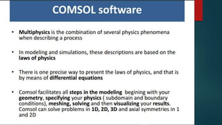
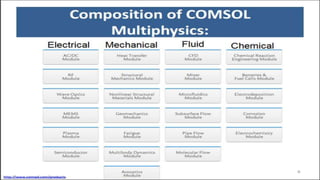

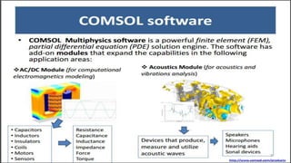
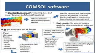
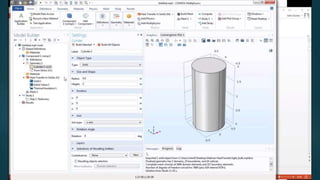
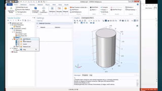
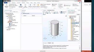
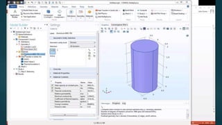
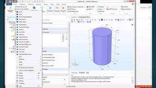
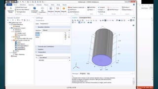
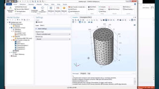
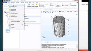
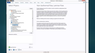
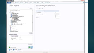
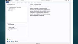
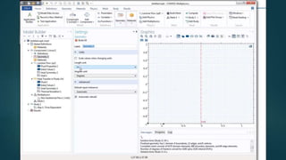
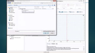
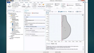
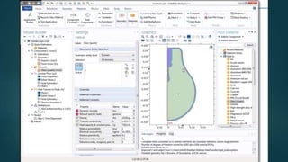
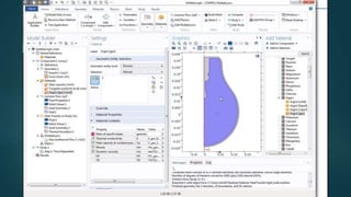
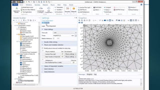
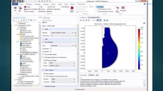
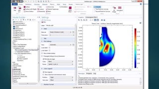
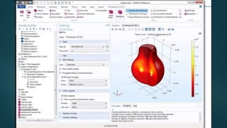
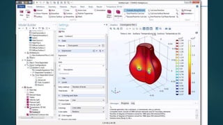
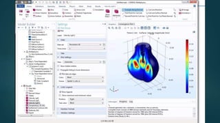
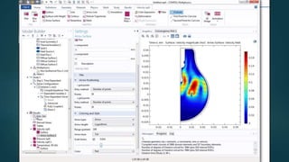
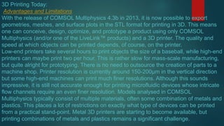
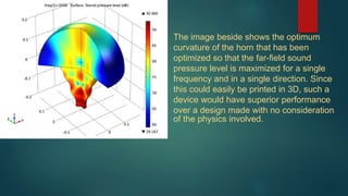


The seminar presented by Manish Kumar Shaw focused on COMSOL Multiphysics, a software for finite element analysis and simulation across various engineering applications. Notable features include its ability to handle coupled systems of partial differential equations, the introduction of custom user interfaces, and integration with MATLAB. The discussion also highlighted advancements in 3D printing capabilities with the software, allowing for design optimization and prototyping directly related to the physics involved.