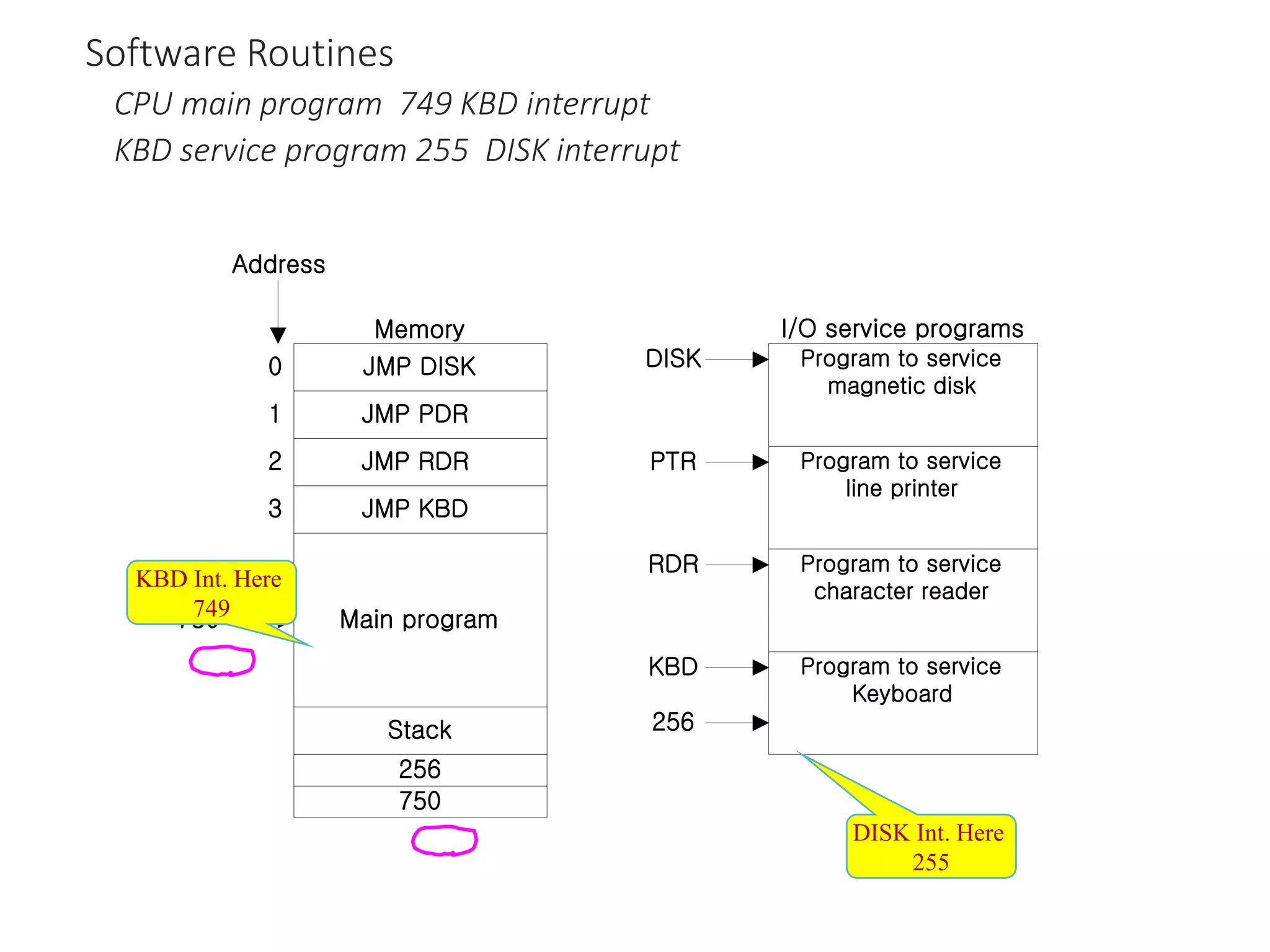
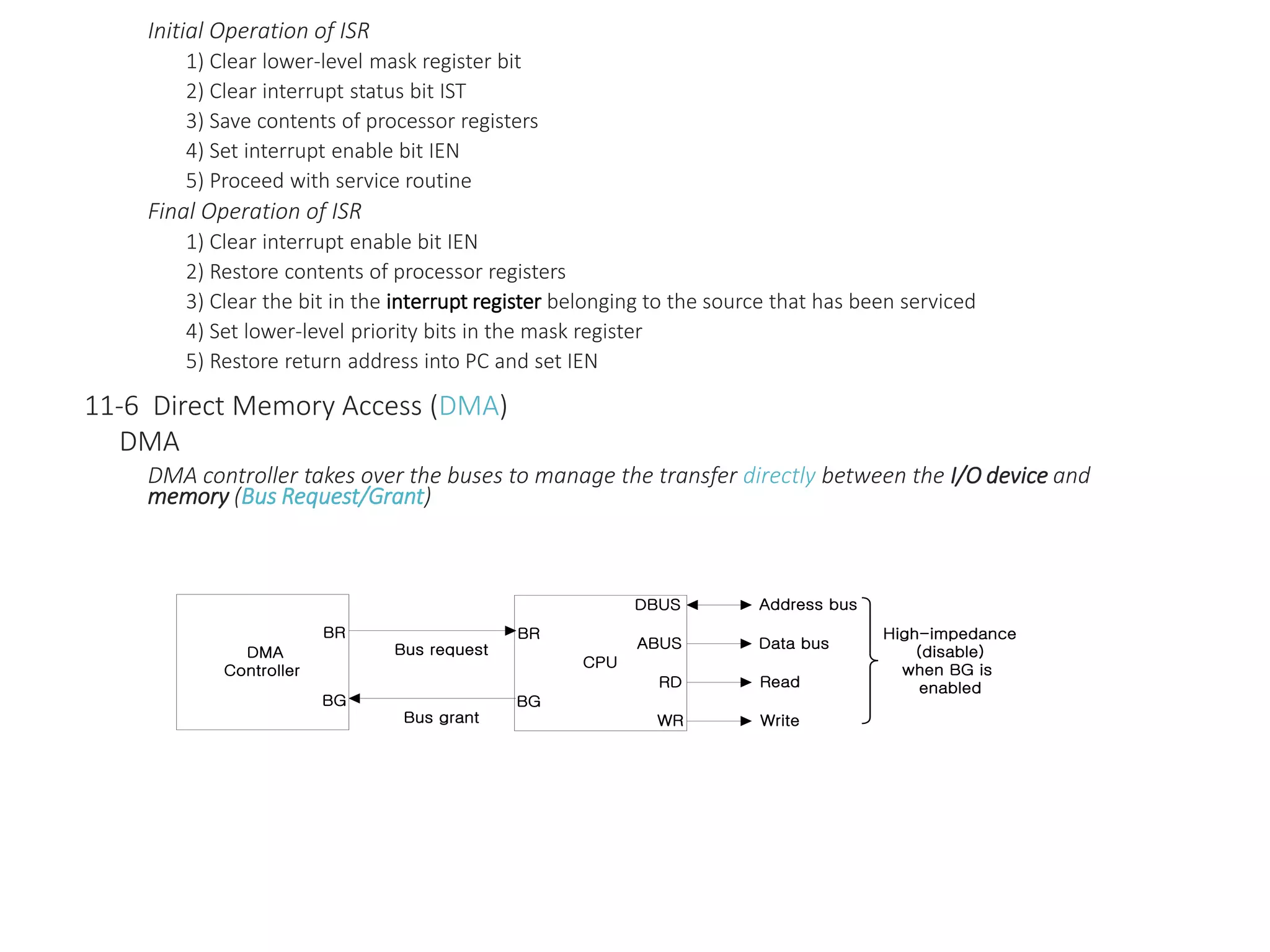
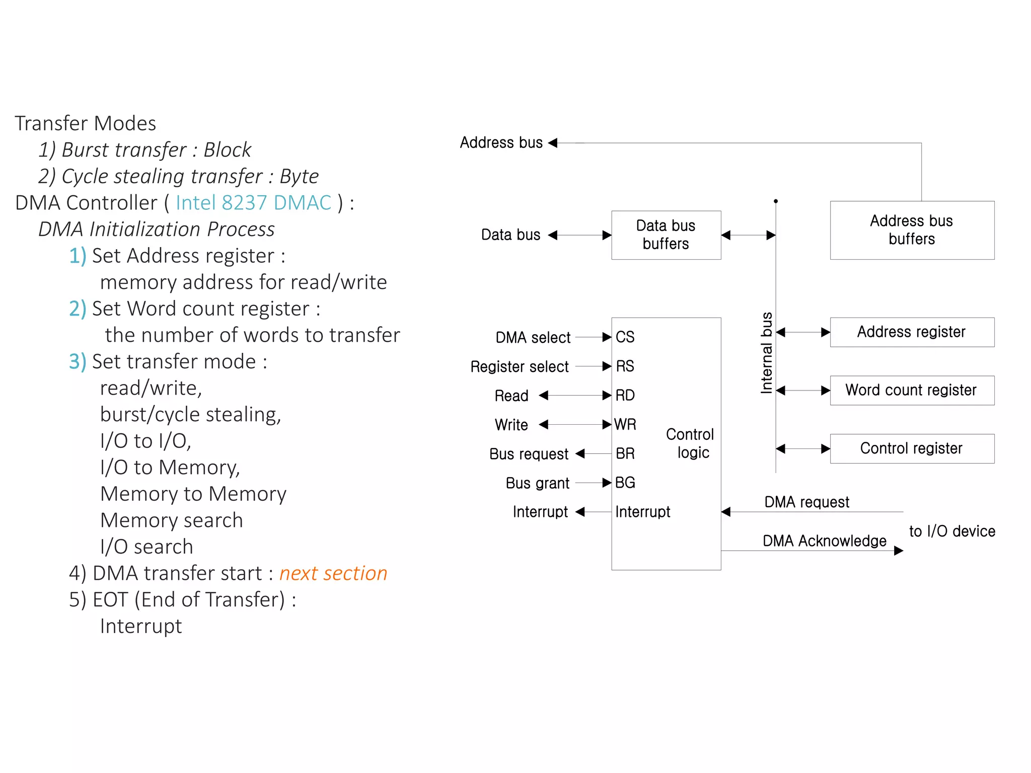
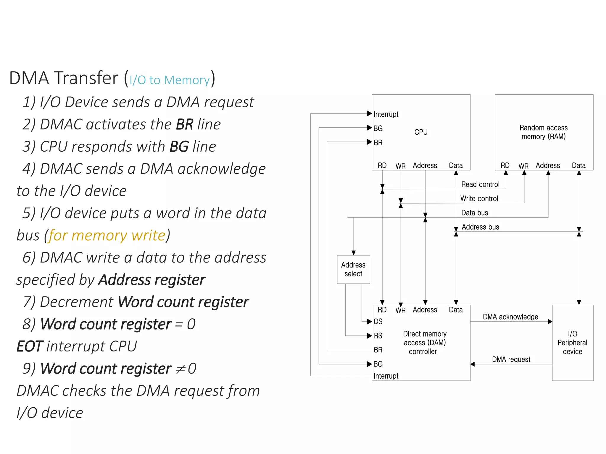
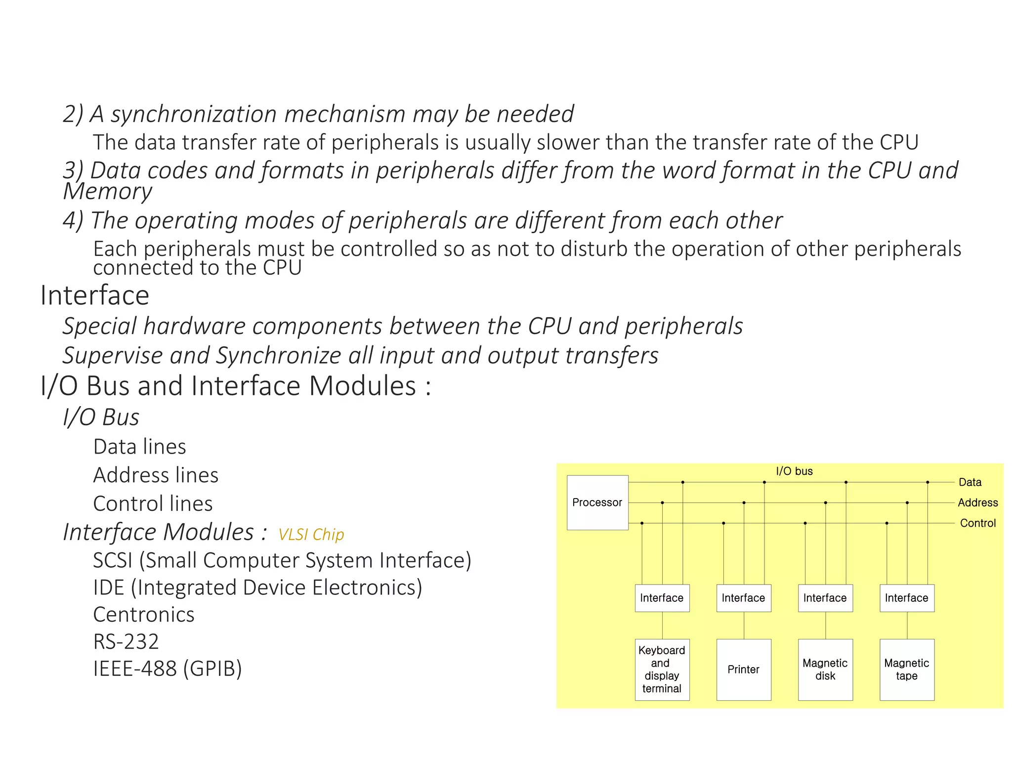
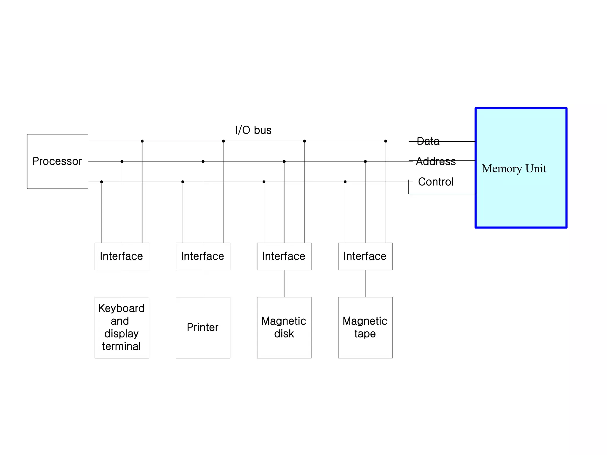
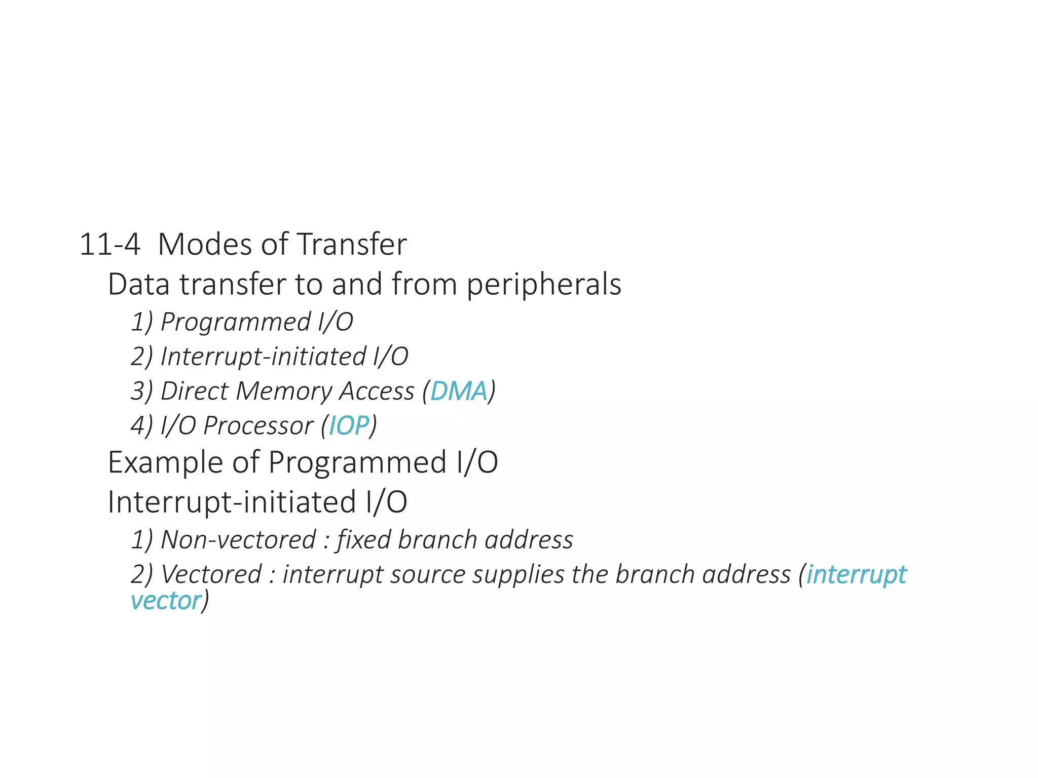
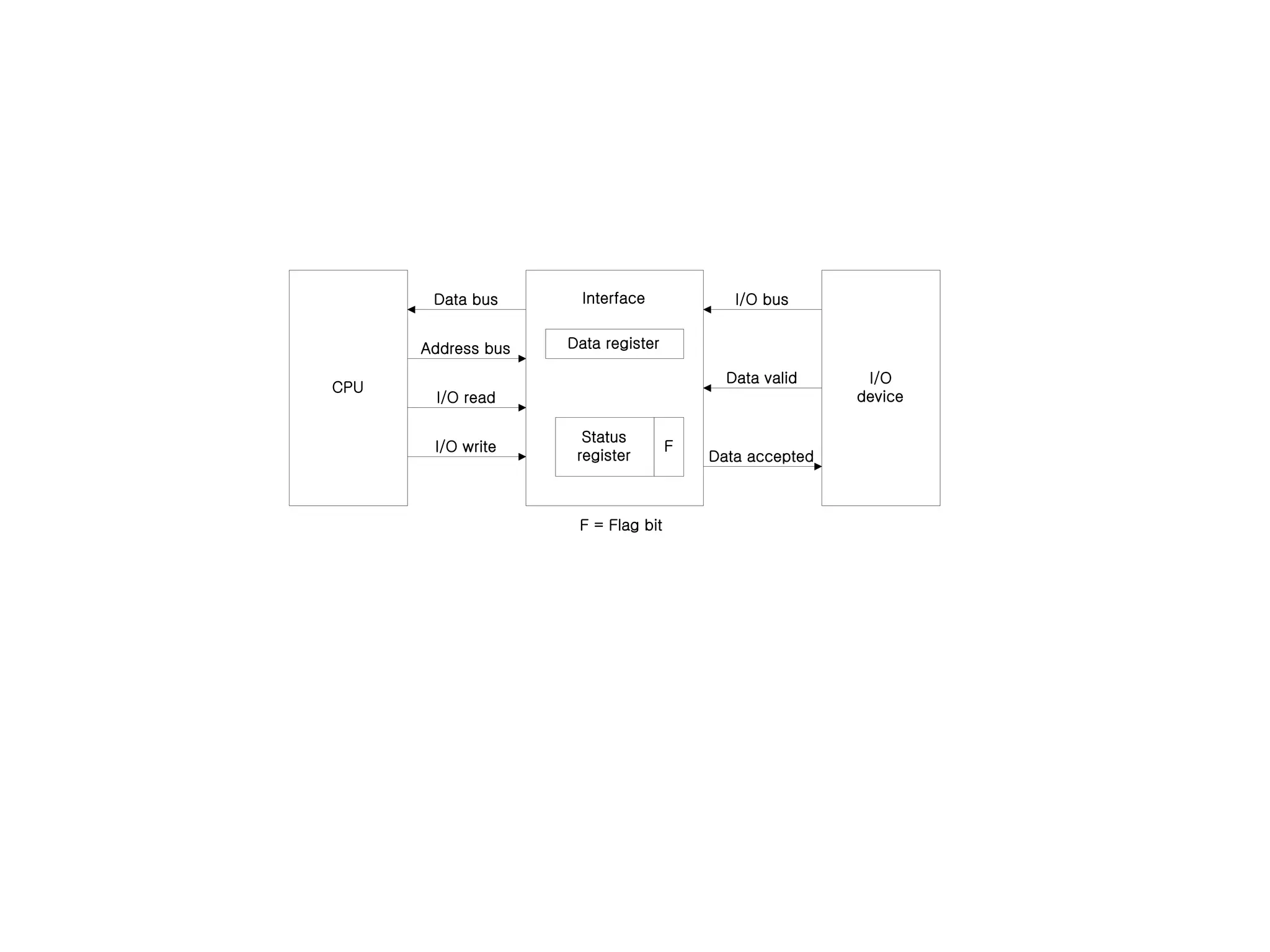
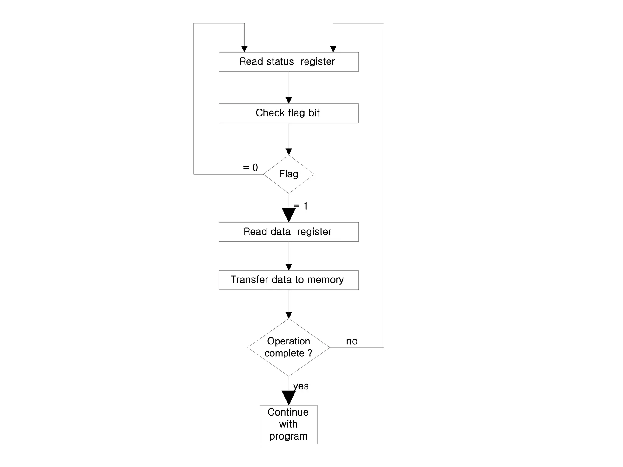
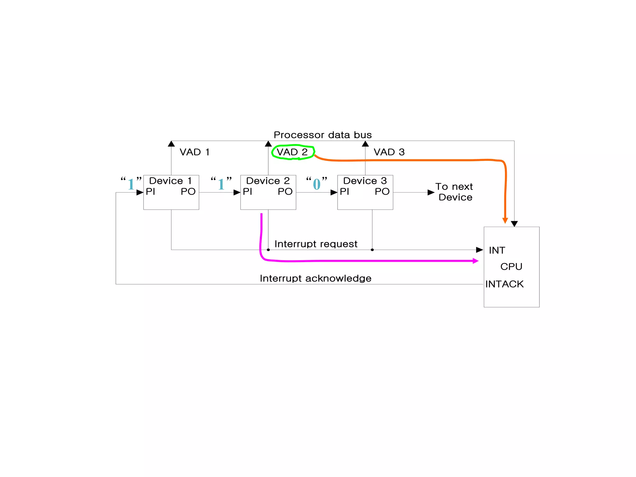
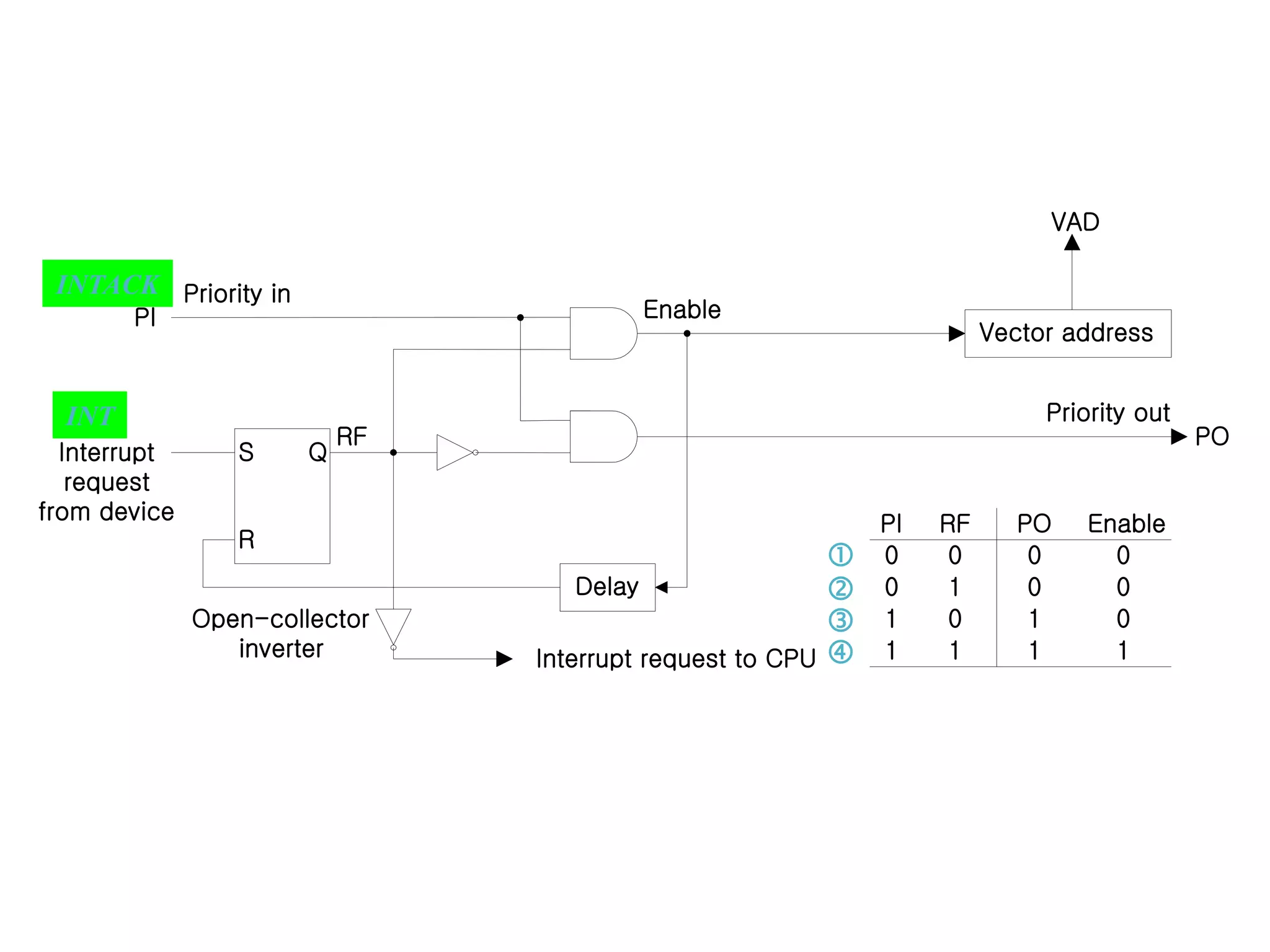
Input-Output
Organization
MCA-05/MSCIT-05/PGDCA-05/BCA-11
Input-Output Organization
11-1 Peripheral Devices
I/O Subsystem
Provides an efficient mode of communication between the central system and the outside environment
Peripheral (or I/O Device)
Input or Output devices attached to the computer
Monitor (Visual Output Device) : CRT, LCD
KBD (Input Device) : light pen, mouse, touch screen, joy stick, digitizer
Printer (Hard Copy Device) : Dot matrix (impact), thermal, ink jet, laser (non-impact)
Storage Device : Magnetic tape, magnetic disk, optical disk
11-2 Input-Output Interface
Interface
1) A conversion of signal values may be required
2) A synchronization mechanism may be needed
The data transfer rate of peripherals is usually slower than the transfer rate of the CPU
3) Data codes and formats in peripherals differ from the word format in the CPU and Memory
4) The operating modes of peripherals are different from each other
Each peripherals must be controlled so as not to disturb the operation of other peripherals connected to the CPU
2) A synchronization mechanism may be needed
The data transfer rate of peripherals is usually slower than the transfer rate of the CPU
3) Data codes and formats in peripherals differ from the word format in the CPU and
Memory
4) The operating modes of peripherals are different from each other
Each peripherals must be controlled so as not to disturb the operation of other peripherals
connected to the CPU
Interface
Special hardware components between the CPU and peripherals
Supervise and Synchronize all input and output transfers
I/O Bus and Interface Modules :
I/O Bus
Data lines
Address lines
Control lines
Interface Modules : VLSI Chip
SCSI (Small Computer System Interface)
IDE (Integrated Device Electronics)
Centronics
RS-232
IEEE-488 (GPIB)
Interface
Keyboard
and
display
terminal
Interface
Magnetic
tape
Interface
Magnetic
disk
Interface
Printer
Processor
Data
Control
Address
I/O bus
Interface
Keyboard
and
display
terminal
Interface
Magnetic
tape
Interface
Magnetic
disk
Interface
Printer
Processor
Data
Control
Address
I/O bus
Memory Unit
I/O command :
1. Control Command
2. Status Command
3. Input Command
4. Output Command
I/O Bus versus Memory Bus
Computer buses can be used to communicate with memory and I/O
1) Use two separate buses, one for memory and the other for I/O
I/O Processor
2) Use one common bus for both memory and I/O but have separate control
lines for each : Isolated I/O or I/O Mapped I/O
Example of I/O Interface :
4 I/O port : Data port A, Data port B, Control,
Status
8255 PIO ( port A, B, C, Control/Status )
Address Decode : CS, RS1, RS0
11-3 Asynchronous Data Transfer
Synchronous Data Transfer
All data transfers occur simultaneously during
the occurrence of a clock pulse
Registers in the interface share a common clock
with CPU registers
Asynchronous Data Transfer
Internal timing in each unit (CPU and Interface)
is independent
Each unit uses its own private clock for internal
registers
Timing
and
Control
CS
WR
RD
RS
0
RS
1
Bus
buffers
Status
register
Control
register
Port B
register
Port A
register
Bidirectional
data bus
Status
To CPU
I/O read
Register select
Chip select
I/O write
I/O data
I/O data
Control
To I/O device
Internal
bus
CS RS
0
RS
1
Register selected
None : data bus in high-impedance
Port A register
Port B register
Control register
Status register
0
1
1
1
1
1 0
0
1
1
0
1
0
× ×
11-4 Modes of Transfer
Data transfer to and from peripherals
1) Programmed I/O
2) Interrupt-initiated I/O
3) Direct Memory Access (DMA)
4) I/O Processor (IOP)
Example of Programmed I/O
Interrupt-initiated I/O
1) Non-vectored : fixed branch address
2) Vectored : interrupt source supplies the branch address (interrupt
vector)
Interface
CPU
I/O
device
Data register
Status
register
F
Data bus
I/O write
I/O read
Address bus
Data accepted
Data valid
I/O bus
F = Flag bit
Read status register
Check flag bit
Read data register
Transfer data to memory
Continue
with
program
Flag
Operation
complete ?
= 0
= 1
yes
no
Software Considerations
I/O routines
software routines for controlling peripherals and for transfer of data between the processor and
peripherals
I/O routines for standard peripherals are provided by the manufacturer (Device driver, OS or BIOS)
I/O routines are usually included within the operating system
I/O routines are usually available as operating system procedures ( OS or BIOS function call)
11-5 Priority Interrupt
Priority Interrupt
Identify the source of the interrupt when several sources will request service simultaneously
Determine which condition is to be serviced first when two or more requests arrive simultaneously
:
1) Software : Polling
2) Hardware : Daisy chain, Parallel priority
Polling
Identify the highest-priority source by software means
One common branch address is used for all interrupts
Program polls the interrupt sources in sequence
The highest-priority source is tested first
Polling priority interrupt
If there are many interrupt sources, the time required to poll them can
exceed the time available to service the I/O device
Hardware priority interrupt
Daisy-Chaining :
Device 2
Interrupt Request
Device 1
PI PO
Device 3
PI PO
Device 2
PI PO
To next
Device
CPU
INT
INTACK
Interrupt request
Interrupt acknowledge
Processor data bus
VAD 1 VAD 3
VAD 2
“1” “1” “0”
One stage of the daisy-chain priority arrangement :
 No interrupt request
 Invalid : interrupt request, but no acknowledge
 No interrupt request : Pass to other device (other device requested
interrupt )
 Interrupt request
S Q
R
Vector address
Delay
Enable
RF
PI
Priority in
Interrupt
request
from device
Open-collector
inverter Interrupt request to CPU
Priority out
PO
VAD
RF
PI PO Enable
0
0
1
1
0
0
1
1
0
0
1
1
0
0
0
1




INTACK
INT
Parallel Priority
Priority Encoder Parallel Priority :
Interrupt Enable F/F (IEN) : set or cleared by
the program
Interrupt Status F/F (IST) : set or cleared by
the encoder output
Priority Encoder Truth Table :
I0
Interrupt Cycle
At the end of each instruction cycle, CPU
checks IEN and IST
if both IEN and IST equal to “1”
CPU goes to an Instruction Cycle
Sequence of microoperation during
Instruction Cycle
0
3
2
1
0
3
2
1
Priority
encoder
I0
I2
I3
I1
disk
Keyboard
Reade
r
Printer
Interrupt
register
y
0
0
0
0
0
0
x
IST
IEN
VAD
to CPU
Enable
Interrupt
to CPU
INTACK
from CPU
Mask
register
n
instructio
next
Fetch
to
0
1
]
[
1
Go
IEN
VAD
PC
INTACK
PC
SP
M
SP
SP




−

: Decrement stack point
: Push PC into stack
: Enable INTACK
: Transfer VAD to PC
: Disable further interrupts
Software Routines
CPU main program 749 KBD interrupt
KBD service program 255 DISK interrupt
JMP DISK
Main program
JMP KBD
JMP RDR
JMP PDR
Stack
750
256
Memory
0
3
2
1
Address
750
Program to service
magnetic disk
Program to service
Keyboard
Program to service
character reader
Program to service
line printer
DISK
256
KBD
RDR
PTR
I/O service programs
KBD Int. Here
749
DISK Int. Here
255
Initial Operation of ISR
1) Clear lower-level mask register bit
2) Clear interrupt status bit IST
3) Save contents of processor registers
4) Set interrupt enable bit IEN
5) Proceed with service routine
Final Operation of ISR
1) Clear interrupt enable bit IEN
2) Restore contents of processor registers
3) Clear the bit in the interrupt register belonging to the source that has been serviced
4) Set lower-level priority bits in the mask register
5) Restore return address into PC and set IEN
11-6 Direct Memory Access (DMA)
DMA
DMA controller takes over the buses to manage the transfer directly between the I/O device and
memory (Bus Request/Grant)
CPU
BR
BG
DBUS
WR
ABUS
RD
Bus request
Bus grant
Address bus
Write
Read
Data bus
High-impedance
(disable)
when BG is
enabled
DMA
Controller
BR
BG
Transfer Modes
1) Burst transfer : Block
2) Cycle stealing transfer : Byte
DMA Controller ( Intel 8237 DMAC ) :
DMA Initialization Process
1) Set Address register :
memory address for read/write
2) Set Word count register :
the number of words to transfer
3) Set transfer mode :
read/write,
burst/cycle stealing,
I/O to I/O,
I/O to Memory,
Memory to Memory
Memory search
I/O search
4) DMA transfer start : next section
5) EOT (End of Transfer) :
Interrupt
Control
logic
CS
Data bus
buffers
Control register
Data bus
DMA select
Internal
bus
RS
Interrupt
BG
BR
RD
WR
Register select
Read
Write
Bus request
Bus grant
Interrupt
Address register
Word count register
Address bus
buffers
Address bus
DMA request
DMA Acknowledge
to I/O device
DMA Transfer (I/O to Memory)
1) I/O Device sends a DMA request
2) DMAC activates the BR line
3) CPU responds with BG line
4) DMAC sends a DMA acknowledge
to the I/O device
5) I/O device puts a word in the data
bus (for memory write)
6) DMAC write a data to the address
specified by Address register
7) Decrement Word count register
8) Word count register = 0
EOT interrupt CPU
9) Word count register  0
DMAC checks the DMA request from
I/O device
I/O
Peripheral
device
DMA acknowledge
Address
select
CPU
Interrupt
Address Data
BG
BR
RD WR
Random access
memory (RAM)
Address Data
RD WR
Direct memory
access (DAM)
controller
Interrupt
Address Data
RD WR
BG
RS
DS
BR
DMA request
Read control
Write control
Address bus
Data bus
Reference
Mano, M. Morris (October 1992). Computer System
Architecture (3rd ed.). Prentice-Hall. ISBN 0-13-175563-3
Lecture notes of Dept. of Info. & Comm., Korea Univ. of Tech. &
Edu., Korea

Computer organization part 2

  • 1.
  • 2.
    Input-Output Organization 11-1 PeripheralDevices I/O Subsystem Provides an efficient mode of communication between the central system and the outside environment Peripheral (or I/O Device) Input or Output devices attached to the computer Monitor (Visual Output Device) : CRT, LCD KBD (Input Device) : light pen, mouse, touch screen, joy stick, digitizer Printer (Hard Copy Device) : Dot matrix (impact), thermal, ink jet, laser (non-impact) Storage Device : Magnetic tape, magnetic disk, optical disk 11-2 Input-Output Interface Interface 1) A conversion of signal values may be required 2) A synchronization mechanism may be needed The data transfer rate of peripherals is usually slower than the transfer rate of the CPU 3) Data codes and formats in peripherals differ from the word format in the CPU and Memory 4) The operating modes of peripherals are different from each other Each peripherals must be controlled so as not to disturb the operation of other peripherals connected to the CPU
  • 3.
    2) A synchronizationmechanism may be needed The data transfer rate of peripherals is usually slower than the transfer rate of the CPU 3) Data codes and formats in peripherals differ from the word format in the CPU and Memory 4) The operating modes of peripherals are different from each other Each peripherals must be controlled so as not to disturb the operation of other peripherals connected to the CPU Interface Special hardware components between the CPU and peripherals Supervise and Synchronize all input and output transfers I/O Bus and Interface Modules : I/O Bus Data lines Address lines Control lines Interface Modules : VLSI Chip SCSI (Small Computer System Interface) IDE (Integrated Device Electronics) Centronics RS-232 IEEE-488 (GPIB) Interface Keyboard and display terminal Interface Magnetic tape Interface Magnetic disk Interface Printer Processor Data Control Address I/O bus
  • 4.
  • 5.
    I/O command : 1.Control Command 2. Status Command 3. Input Command 4. Output Command I/O Bus versus Memory Bus Computer buses can be used to communicate with memory and I/O 1) Use two separate buses, one for memory and the other for I/O I/O Processor 2) Use one common bus for both memory and I/O but have separate control lines for each : Isolated I/O or I/O Mapped I/O
  • 6.
    Example of I/OInterface : 4 I/O port : Data port A, Data port B, Control, Status 8255 PIO ( port A, B, C, Control/Status ) Address Decode : CS, RS1, RS0 11-3 Asynchronous Data Transfer Synchronous Data Transfer All data transfers occur simultaneously during the occurrence of a clock pulse Registers in the interface share a common clock with CPU registers Asynchronous Data Transfer Internal timing in each unit (CPU and Interface) is independent Each unit uses its own private clock for internal registers
  • 7.
    Timing and Control CS WR RD RS 0 RS 1 Bus buffers Status register Control register Port B register Port A register Bidirectional databus Status To CPU I/O read Register select Chip select I/O write I/O data I/O data Control To I/O device Internal bus CS RS 0 RS 1 Register selected None : data bus in high-impedance Port A register Port B register Control register Status register 0 1 1 1 1 1 0 0 1 1 0 1 0 × ×
  • 8.
    11-4 Modes ofTransfer Data transfer to and from peripherals 1) Programmed I/O 2) Interrupt-initiated I/O 3) Direct Memory Access (DMA) 4) I/O Processor (IOP) Example of Programmed I/O Interrupt-initiated I/O 1) Non-vectored : fixed branch address 2) Vectored : interrupt source supplies the branch address (interrupt vector)
  • 9.
    Interface CPU I/O device Data register Status register F Data bus I/Owrite I/O read Address bus Data accepted Data valid I/O bus F = Flag bit
  • 10.
    Read status register Checkflag bit Read data register Transfer data to memory Continue with program Flag Operation complete ? = 0 = 1 yes no
  • 11.
    Software Considerations I/O routines softwareroutines for controlling peripherals and for transfer of data between the processor and peripherals I/O routines for standard peripherals are provided by the manufacturer (Device driver, OS or BIOS) I/O routines are usually included within the operating system I/O routines are usually available as operating system procedures ( OS or BIOS function call) 11-5 Priority Interrupt Priority Interrupt Identify the source of the interrupt when several sources will request service simultaneously Determine which condition is to be serviced first when two or more requests arrive simultaneously : 1) Software : Polling 2) Hardware : Daisy chain, Parallel priority
  • 12.
    Polling Identify the highest-prioritysource by software means One common branch address is used for all interrupts Program polls the interrupt sources in sequence The highest-priority source is tested first Polling priority interrupt If there are many interrupt sources, the time required to poll them can exceed the time available to service the I/O device Hardware priority interrupt Daisy-Chaining : Device 2 Interrupt Request
  • 13.
    Device 1 PI PO Device3 PI PO Device 2 PI PO To next Device CPU INT INTACK Interrupt request Interrupt acknowledge Processor data bus VAD 1 VAD 3 VAD 2 “1” “1” “0”
  • 14.
    One stage ofthe daisy-chain priority arrangement :  No interrupt request  Invalid : interrupt request, but no acknowledge  No interrupt request : Pass to other device (other device requested interrupt )  Interrupt request
  • 15.
    S Q R Vector address Delay Enable RF PI Priorityin Interrupt request from device Open-collector inverter Interrupt request to CPU Priority out PO VAD RF PI PO Enable 0 0 1 1 0 0 1 1 0 0 1 1 0 0 0 1     INTACK INT
  • 16.
    Parallel Priority Priority EncoderParallel Priority : Interrupt Enable F/F (IEN) : set or cleared by the program Interrupt Status F/F (IST) : set or cleared by the encoder output Priority Encoder Truth Table : I0 Interrupt Cycle At the end of each instruction cycle, CPU checks IEN and IST if both IEN and IST equal to “1” CPU goes to an Instruction Cycle Sequence of microoperation during Instruction Cycle
  • 17.
    0 3 2 1 0 3 2 1 Priority encoder I0 I2 I3 I1 disk Keyboard Reade r Printer Interrupt register y 0 0 0 0 0 0 x IST IEN VAD to CPU Enable Interrupt to CPU INTACK fromCPU Mask register n instructio next Fetch to 0 1 ] [ 1 Go IEN VAD PC INTACK PC SP M SP SP     −  : Decrement stack point : Push PC into stack : Enable INTACK : Transfer VAD to PC : Disable further interrupts
  • 18.
    Software Routines CPU mainprogram 749 KBD interrupt KBD service program 255 DISK interrupt JMP DISK Main program JMP KBD JMP RDR JMP PDR Stack 750 256 Memory 0 3 2 1 Address 750 Program to service magnetic disk Program to service Keyboard Program to service character reader Program to service line printer DISK 256 KBD RDR PTR I/O service programs KBD Int. Here 749 DISK Int. Here 255
  • 19.
    Initial Operation ofISR 1) Clear lower-level mask register bit 2) Clear interrupt status bit IST 3) Save contents of processor registers 4) Set interrupt enable bit IEN 5) Proceed with service routine Final Operation of ISR 1) Clear interrupt enable bit IEN 2) Restore contents of processor registers 3) Clear the bit in the interrupt register belonging to the source that has been serviced 4) Set lower-level priority bits in the mask register 5) Restore return address into PC and set IEN 11-6 Direct Memory Access (DMA) DMA DMA controller takes over the buses to manage the transfer directly between the I/O device and memory (Bus Request/Grant) CPU BR BG DBUS WR ABUS RD Bus request Bus grant Address bus Write Read Data bus High-impedance (disable) when BG is enabled DMA Controller BR BG
  • 20.
    Transfer Modes 1) Bursttransfer : Block 2) Cycle stealing transfer : Byte DMA Controller ( Intel 8237 DMAC ) : DMA Initialization Process 1) Set Address register : memory address for read/write 2) Set Word count register : the number of words to transfer 3) Set transfer mode : read/write, burst/cycle stealing, I/O to I/O, I/O to Memory, Memory to Memory Memory search I/O search 4) DMA transfer start : next section 5) EOT (End of Transfer) : Interrupt Control logic CS Data bus buffers Control register Data bus DMA select Internal bus RS Interrupt BG BR RD WR Register select Read Write Bus request Bus grant Interrupt Address register Word count register Address bus buffers Address bus DMA request DMA Acknowledge to I/O device
  • 21.
    DMA Transfer (I/Oto Memory) 1) I/O Device sends a DMA request 2) DMAC activates the BR line 3) CPU responds with BG line 4) DMAC sends a DMA acknowledge to the I/O device 5) I/O device puts a word in the data bus (for memory write) 6) DMAC write a data to the address specified by Address register 7) Decrement Word count register 8) Word count register = 0 EOT interrupt CPU 9) Word count register  0 DMAC checks the DMA request from I/O device I/O Peripheral device DMA acknowledge Address select CPU Interrupt Address Data BG BR RD WR Random access memory (RAM) Address Data RD WR Direct memory access (DAM) controller Interrupt Address Data RD WR BG RS DS BR DMA request Read control Write control Address bus Data bus
  • 22.
    Reference Mano, M. Morris(October 1992). Computer System Architecture (3rd ed.). Prentice-Hall. ISBN 0-13-175563-3 Lecture notes of Dept. of Info. & Comm., Korea Univ. of Tech. & Edu., Korea