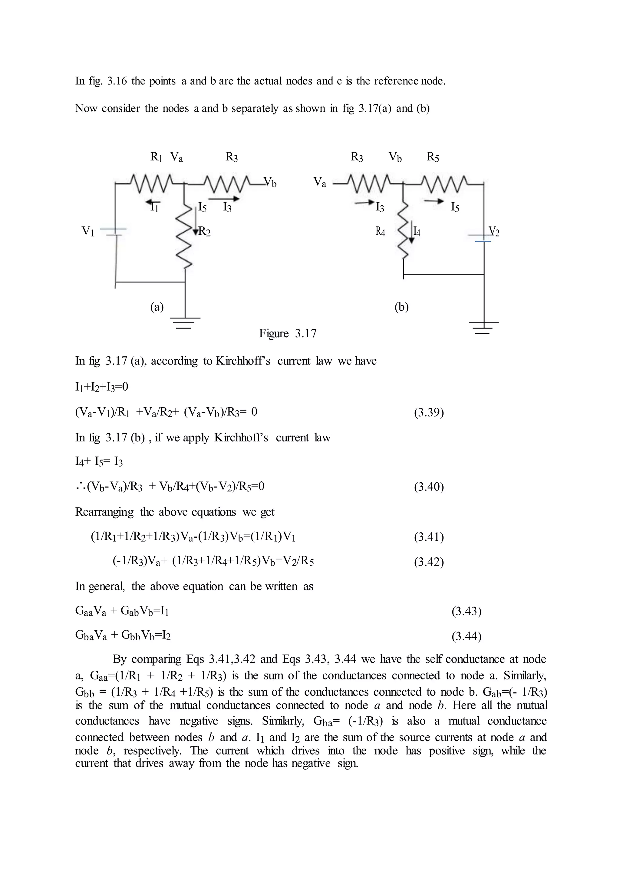
Circuit and Network Theory
Contributors:-
Biswaranjan mohapatra
INDEX
Sl. Contents
No.
1 Circuit Element and Laws
2 Magnetic circuit
3 Network Analysis
4 Network Theorems
5 A.C. Circuit and Resonance
6 Coupled Circuit
7 Transients
8 Two Port Network
9 Filters
CHAPTER 1
Circuit Elements and Laws
1.1 Voltage
Energy is required for the movement of charge from one point to another. Let W
Joules of energy be required to move positive charge Q columbs from a point a to
point b in a circuit. We say that a voltage exists between the two points. The voltage
V between two points may be defined in terms of energy that would be required if a
charge were transferred from one point to the other. Thus, there can be a voltage
between two points even if no charge is actually moving from one to the other.
Voltage between a and b is given by
V =
W
Q J / C
Hence Electric Potential (V) =
Worked are (W) in Joules
Ch arg e (Q)in columbs
Current :
An electric current is the movement of electric charges along a definite path. In case
of a conductor the moving charges are electrons.
The unit of current is the ampere. The ampere is defined as that current which when
flowing in two infinitely long parallel conductors of negligible cross section, situated 1 meter
apart in Vacuum, produces between the conductors a force of 2 x 10⁻⁷
Newton per metre
length.
Power : Power is defined as the work done per unit time. If a field F newton acts for t
seconds through a distance d metres along a straight line, work done W = Fxd N.m. or J. The
power P, either generated or dissipated by the circuit element.
P = w = F x d
t t
Power can also be written as Power =
Work
time
= Ch
Work
arge x
Ch
Time
arge
=
Voltage x Current P = V x I watt.
Energy : Electric energy W is defined as the Power Consumed in a given time. Hence, if
current IA flows in an element over a time period t second, when a voltage V volts is applied
across it, the energy consumed is given by
W = P x t = V x I x t J or watt. second.
The unit of energy W is Joule (J) or watt. second. However, in practice, the unit of
energy is kilowatt. hour (Kwh)
1.2 Resistance : According to Ohm's law potential difference (V) across the ends of a
conductor is proportional to the current (I) flowing through the conductor at a
constant temperature. Mathematically Ohm's law is expressed as
Vα I or V = R x I
Or R =
V
I where R is the proportionality constant and is designated as the conductor
resistance and has the unit of Ohm (Ω).
Conductance : Voltage is induced in a stationary conductor when placed in a varying
magnetic field. The induced voltage (e) is proportional to the time rate of change of
current, di/dt producing the magnetic field.
Therefore e α dt
di
Or e = L dt
di
e and i are both function of time. The proportionality constant L is called inductance.
The Unit of inductance is Henery (H).
Capacitance : A capacitor is a Physical device, which when polarized by an electric field by
applying a suitable voltage across it, stores energy in the form of a charge separation.
The ability of the capacitor to store charge is measured in terms of capacitance.
Capacitence of a capacitor is defined as the charge stored per Volt applied.
C =
q
=
Coulomb
= Farad
v Volt
1.3 Active and passive Branch :
A branch is said to be active when it contains one or more energy sources. A passive
branch does not contain an energy source.
Branch : A branch is an element of the network having only two terminals.
Bilateral and unilateral element :
A bilateral element conducts equally well in either direction. Resistors and inductors
are examples of bilateral elements. When the current voltage relations are different for
the two directions of current flow, the element is said to be unilateral. Diode is an
unilateral element.
Linear Elements : When the current and voltage relationship in an element can be
simulated by a linear equation either algebraic, differential or integral type, the
element is said to be linear element.
Non Linear Elements : When the current and voltage relationship in an element can
not be simulated by a linear equation, the element is said to be non linear elements.
1.4 Kirchhoff's Voltage Law (KVL) :
The algebraic sum of Voltages (or voltage drops) in any closed path or loop is Zero.
Application of KVL with series connected voltage source.
Fig. 1.1
V1 + V2 – IR1 – IR2 = 0
= V1 + V2 = I (R1 + R2)
I =
V
1 + V2
R1 + R 2
Application of KVL while voltage sources are connected in opposite polarity.
Fig. 1.2
V1 – IR1 – V2 – IR2 – IR3 = 0
¾ V1 – V2 = IR1 + IR2 + IR3
¾ V1 – V2 = I (R1 + IR2 + IR3)
¾ I =
V1 − V2
R1 + R 2 + R 3
Kirchaoff's Current Law (KCL) :
The algebraic sum of currents meeting at a junction or mode is zero.
Fig. 1.3
Considering five conductors, carrying currents I1, I2, I3, I4 and I5 meeting at a point O.
Assuming the incoming currents to be positive and outgoing currents negative.
I1 + (-I2) + I3 + (-I4) + I5 = 0
I1 – I2 + I3 – I4 + I5 = 0
I1 + I3 + I5 = I2 + I4
Thus above Law can also be stated as the sum of currents flowing towards any
junction in an electric circuit is equal to the sum of the currents flowing away from
that junction.
Voltage Division (Series Circuit)
Considering a voltage source (E) with resistors R1 and R2 in series across it.
Fig. 1.4
I =
E
R1 + R2
Voltage drop across R1 = I. R1 =
E.R1
R1 + R2
Similarly voltage drop across R2 = I.R2 =
E.R1
R1 + R2
Current Division :
A parallel circuit acts as a current divider as the current divides in all branches in a
parallel circuit.
Fig. 1.5
Fig. shown the current I has been divided into I1 and I2 in two parallel branches with
resistances R1 and R2 while V is the voltage drop across R1 and R2.
I1 =
V
and I2 =
V
R1 R 2
Let R = Total resistance of the circuit.
Hence 1 = = 1 + 1
R R1 R 2
¾ R =
R1R 2
R1 + R2
I =
V
=
V
=
V(R1 + R2 )
R
R
1
R
2
R1R2
R1 + R2
But = V = I1R1 = I2R2
R
1
R
2
¾ I = I1R1
+ R 2
R
1
¾ I =
I1 (R1 + R2 )
R2
Therefore I1 =
IR2
R1 + R2
Similarly it can be derived that
I2 =
IR1
R1 + R 2
CHAPTER 2
Magnetic Circuits :
Introduction : Magnetic flux lines always form closed loops. The closed path
followed by the flux lines is called a magnetic circuit. Thus, a magnetic circuit
provides a path for magnetic flux, just as an electric circuit provides a path for the
flow of electric current. In general, the term magnetic circuit applies to any closed
path in space, but in the analysis of electro-mechanical and electronic system this term
is specifically used for circuits containing a major portion of ferromagnetic materials.
The study of magnetic circuit concepts is essential in the design, analysis and
application of electromagnetic devices like transformers, rotating machines,
electromagnetic relays etc.
Magnetomotive Force (M.M.F) :
Flux is produced round any current – carrying coil. In order to produce the required
flux density, the coil should have the correct number of turns. The product of the
current and the number of turns is defined as the coil magneto motive force (m.m.f).
If I = Current through the coil (A)
N = Number of turns in the coil.
Magnetomotive force = Current x turns
So M.M.F = I X N
The unit of M.M.F. is ampere–turn (AT) but it is taken as Ampere(A) since N
has no dimensions.
Magnetic Field Intensity
Magnetic Field Intensity is defined as the magneto-motive force per unit length of the
magnetic flux path. Its symbol is H.
Magnetomotive force
Magnetic field Intensity (H) =
Mean length of the magnetic path
¾ H =
F
l =
I .N
l
.
A/m
Where l is the mean length of the magnetic circuit in meters. Magnetic field intensity is also
called magnetic field strength or magnetizing force.
Permeability :-
Every substance possesses a certain power of conducting magnetic lines
of force. For example, iron is better conductor for magnetic lines of force than
air (vaccum) . Permeability of a material (μ) is its conducting power for
magnetic lines of force. It is the ratio of the flux density. (B) Produced in a
material to the magnetic filed strength (H) i.e. μ =
B
H
Reluctance :
Reluctance (s) is akin to resistance (which limits the electric Current).
Flux in a magnetic circuit is limited by reluctance. Thus reluctance(s) is a
measure of the opposition offered by a magnetic circuit to the setting up of the
flux.
Reluctance is the ratio of magneto motive force to the flux. Thus
S =
Mmf
φ
Its unit is ampere turns per webber (or AT/wb)
Permeance:-
The reciprocal of reluctance is called the permeance (symbol A).
Permeance (A) = 1/S wb/AT
Turn T has no unit.
Hence permeance is expressed in wb/A or Henerys(H).
Electric Field versus Magentic Field.
Similarities
Electric Field
1) Flow of Current (I) 1)
2) Emf is the cause of 2)
flow of current
3) Resistance offered 3)
to the flow of
Current, is called
resistance (R)
Conductance 4)
4) σ = 1 ( )
R
5) Current density is 5)
amperes per square
meter.
6) Current (I) - EMF R
6)
Dissimilarities
Magnetic Field
Flow of flux (∅)
MMf is the cause of
flow of flux
Resistance offered to
the flow of flux, is
called reluctance (S)
Permitivity (μ) =
1
S
Flux density is number
of lines per square
meter.
Flux (∅) =
MMF
S
1) Current actually flows 1) Flux does not actually
in an electric Circuit. flow in a magnetic
circuit.
2) Energy is needed as 2) Energy is initially
long as current flows needed to create the
magnetic flux, but not
to maintain it.
3) Conductanceis 3) Permeability (or
constant and magnetic
independent of current conductance)
strength at a particular depends on the total
temperature. flux for a particular
temperature.
B.H. Curve :
Place a piece of an unmagnetised iron bar AB within the field of a
solenoid to magnetise it. The field H produced by the solenoid, is called
magnetising field, whose value can be altered (increased or decreased) by
changing (increasing or decreasing) the current through the solenoid. If we
increase slowly the value of magnetic field (H) from zero to maximum value,
the value of flux density (B) varies along 1 to 2 as shown in the figure and the
magnetic materials (i.e iron bar) finally attains the maximum value of flux
density (Bm) at point 2 and thus becomes magnetically saturated.
Fig. 2.1
Now if value of H is decreased slowly (by decreasing the current in the
solenoid) the corresponding value of flux density (B) does not decreases along
2-1 but decreases some what less rapidly along 2 to 3. Consequently during the
reversal of magnetization, the value of B is not zero, but is '13' at H= 0. In other
wards, during the period of removal of magnetization force (H), the iron bar is
not completely demagnetized.
In order to demagnetise the iron bar completely, we have to supply the
demagnetisastion force (H) in the opposite direction (i.e. by reserving the
direction of current in the solenoid). The value of B is reduced to zero at point 4,
when H='14'. This value of H required to clear off the residual magnetisation, is
known as coercive force i.e. the tenacity with which the material holds to its
magnetism.
If after obtaining zero value of magnetism, the value of H is made more
negative, the iron bar again reaches, finally a state of magnetic saturation at the
point 5, which represents negative saturation. Now if the value of H is increased
from negative saturation (= '45') to positive saturation ( = '12') a curve '5,6,7,2'
is obtained. The closed loop "2,3,4,5,6,7,2" thus represents one complete cycle
of magnetisation and is known as hysteresis loop.
NETWORK ANALYSIS
Different terms are defined below:
1. Circuit: A circuit is a closed conducting path through which an electric current either
. flow or is intended flow
2. Network: A combination of various electric elements, connected in any manner.
Whatsoever, is called an electric network
3. Node: it is an equipotential point at which two or more circuit elements are joined.
4. Junction: it is that point of a network where three or more circuit elements are joined.
5. Branch: it is a part of a network which lies between junction points.
6. Loop: It is a closed path in a circuit in which no element or node is accounted more than
once.
7. Mesh: It is a loop that contains no other loop within it.
Example 3.1 In this circuit configuration of figure 3.1, obtain the no. of i) circuit elements ii)
nodes iii) junction points iv) branches and v) meshes.
R5
c d
R4 R6
p
R1 V3 R8
a b e
V1 R2 R7
K h
g f
R3 R9 V2
Solution: i) no. of circuit elements = 12 (9 resistors + 3 voltage sources)
ii) no. of nodes =10 (a, b, c, d, e, f, g, h, k, p)
iii) no. of junction points =3 (b, e, h)
iv) no. of branches = 5 (bcde, be, bh, befgh, bakh)
v) no. of meshes = 3 (abhk, bcde, befh)
3.2 MESH ANALYSIS
Mesh and nodal analysis are two basic important techniques used in finding solutions
for a network. The suitability of either mesh or nodal analysis to a particular problem
depends mainly on the number of voltage sources or current sources .If a network has a large
number of voltage sources, it is useful to use mesh analysis; as this analysis requires that all
the sources in a circuit be voltage sources. Therefore, if there are any current sources in a
circuit they are to be converted into equivalent voltage sources,if, on the other hand, the
network has more current sources,nodal analysis is more useful.
Mesh analysis is applicable only for planar networks. For non-planar circuits mesh
analysis is not applicable .A circuit is said to be planar, if it can be drawn on a plane surface
without crossovers. A non-planar circuit cannot be drawn on a plane surface without a
crossover.
Figure 3.2 (a) is a planar circuit. Figure 3.2 (b) is a non-planar circuit and fig. 3.2 (c) is a
planar circuit which looks like a non-planar circuit. It has already been discussed that a loop
is a closed path. A mesh is defined as a loop which does not contain any other loops within it.
To apply mesh analysis, our first step is to check whether the circuit is planar or not and the
second is to select mesh currents. Finally, writing Kirchhoff‘s voltage law equations in terms
of unknowns and solving them leads to the final solution.
(a) (b) (c)
Figure 3.2
Observation of the Fig.3.2 indicates that there are two loops abefa,and bcdeb in the
network .Let us assume loop currents I1 and I2with directions as indicated in the figure.
Considering the loop abefa alone, we observe that current I1 is passing through R1, and (I1-
I2) is passing through R2. By applying Kirchhoff’s voltage law, we can write
Vs. =I1R1+R2(I1-I2) (3.1)
R1 R3
a b c
Vs R2
R4
± I1 I2
f e d
Figure 3.3
Similarly, if we consider the second mesh bcdeb, the current I2 is passing through R3
and R4, and (I2 – I1) is passing through R2. By applying Kirchhoff’s voltage law around the
second mesh, we have
R2 (I2-I1) + R3I2 +R4I2 = 0 (3.2)
By rearranging the above equations,the corresponding mesh current equations are
I1 (R1+R2) - I2R2 =Vs.
-I1R2 +(R2+R3+R 4) I2=0 (3.3)
By solving the above equations, we can find the currents I1 and I2,.If we observe
Fig.3.3, the circuit consists of five branches and four nodes, including the reference node.The
number of mesh currents is equal to the number of mesh equations.
And the number of equations=branches-(nodes-1).in Fig.3.3, the required number of
mesh current would be 5-(4-1)=2.
In general we have B number of branches and N number of nodes including the
reference node than number of linearly independent mesh equations M=B-(N-1).
Example 3.2 Write the mesh
5Ω 10Ω
current equations in the circuit shown 10 V 2Ω
50v
in fig 3.4 and determine the currents.
Figure 3.4
Solution: Assume two mesh currents in the direction as indicated in fig. 3.5. The mesh
current equations are
5 Ω
10 VI1 I2 10 Ω
2 Ω 50V
Figure 3.5
5I1 + 2(I1-I2) = 10
1012 + 2(12-11) + 50= 0 (3.4)
We can rearrange the above equations as
7I1 -2I2 =10
-2I1+12I2 = -50 (3.5)
By solving the above equations, we have I1= 0.25 A, and I2 = -4.125
Here the current in the second mesh I2, is negative; that is the actual current I2 flows opposite
to the assumed direction of current in the circuit of fig .3.5.
Example 3.3 Determine the mesh current I1 in the circuit shown in fig.3.6.
10 Ω 2 Ω
5 Ω I2 + 10 V
I1 1 Ω
50 V ‐
3 Ω 5 V
I3
Figure 3.6
Solution: From the circuit, we can from the following three mesh equations
10I1+5(I1+I2) +3(I1-I3) = 50 (3.6)
2I2 +5(I2+I1) +1(I2+I3) = 10 (3.7)
3(I3-I1) +1(I3+I2) = -5 (3.8)
Rearranging the above equations we get
18I1+5I2-3I3=50 (3.9)
5I1+8I2 + I3=10 (3.10)
-3I1 + I2+ 4I3=-5 (3.11)
According to the Cramer’s rule
50 5 − 3
10 8 1
I1= − 5 1 4 = 1175
− 318 5 356
5 8 1
− 3 1 4
Or I1= 3.3 A Similarly,
18 50 − 3
5 10 1
− 3 − 5 4 = − 355I2=
18 5 − 3 356
5 8 1
− 3 1 4
Or I2=-0.997A (3.12)
18 5 50
5 8 10
I3= − 3 1 − 5
=
525
18 5 − 3 356
5 8 1
− 3 1 4
Or I3=1.47A (3.13)
∴I1=3.3A, I2=-0.997A, I3=1.47A
3.3 MESH EQUATIONS BY INSPECTION METHODThe mesh equations for a general planar network can be written
by inspection without going through thedetailed steps. Consider a three mesh networks as shown in figure 3.7
The loop equation are I1R1+ R2(I1-I2) =V1 R1 R3
R4
V1 I1 R2 I2 V2 I3 R5
Figure 3.7
R2( I2-I1)+I2R3= -V2 3.14
R4I3+R5I3=V2 3.15
Reordering the above equations, we have
(R1+R2)I1-R2I2=V1 3.16
-R2I1+(R2+R3)I2=-V2 3.17
(R4+R5)I3=V2 3.18
The general mesh equations for three mesh resistive network can be written as
R11I1 ± R12I2 ± R13I3= Va 3.19
± R21I1+R22I2 ± R23I3= Vb 3.20
± R31I1 ± R32I2+R33I3= Vc 3.21
By comparing the equations 3.16, 3.17 and 3.18 with equations 3.19, 3.20 and 3.21
respectively, the following observations can be taken into account.
1. The self-resistance in each mesh
2. The mutual resistances between all pairs of meshes and
3. The algebraic sum of the voltages in each mesh.
The self-resistance of loop 1, R11=R1+R2, is the sum of the resistances through which I1
passes.
The mutual resistance of loop 1, R12= -R2, is the sum of the resistances common to loop
currents I1 and I2. If the directions of the currents passing through the common resistances are
the same, the mutual resistance will have a positive sign; and if the directions of the currents
passing through the common resistance are opposite then the mutual resistance will have a
negative sign.
Va=V1 is the voltage which drives the loop 1. Here the positive sign is used if
the direction of the currents is the same as the direction of the source. If the current
direction is opposite to the direction of the source, then the negative sign is used.
Similarly R22=R2+R3 and R33=R4+R5 are the self-resistances of loops 2 and 3
respectively. The mutual resistances R13=0, R21= -R2, R23=0, R31=0, R32=0 are the
sums of the resistances common to the mesh currents indicated in their subscripts.
Vb= -V2, Vc= V2 are the sum of the voltages driving their respective loops.
Example 3.4 write the mesh equation for the circuit shown in fig. 3.8
1 Ω 2Ω
3Ω I2 5Ω
+ 5V
I1 _ +
10V - I3 4Ω
6Ω
-
+ -20V
(3.22)
(3.23)
(3.24)
Figure 3.8
Solution : the general equation for three mesh equation are
R11I1 ± R12I2 ± R13I3=Va
± R21I1+R22I2 ± R23I3=Vb
± R31I1 ± R32I2+R33I3=Vc
Consider equation 3.22
R11=self resistance of loop 1=(1Ω+ 3 Ω +6 Ω) =10 Ω
R12= the mutual resistance common to loop 1 and loop 2 = -3 Ω
Here the negative sign indicates that the currents are in opposite direction .
R13= the mutual resistance common to loop 1 & 3= -6 Ω
Va= +10 V, the voltage the driving the loop 1.
Here he positive sign indicates the loop current I1 is in the same direction as the
source element.
Therefore equation 3.22 can be written as
10 I1- 3I2-6I3= 10 V (3.25)
Consider Eq. 3.23
R21= the mutual resistance common to loop 1 and loop 2 = -3 Ω
R22= self resistance of loop 2=(3Ω+ 2 Ω +5 Ω) =10 Ω
R23=0, there is no common resistance between loop 2 and 3.
Vb = -5 V, the voltage driving the loop 2.
Therefore Eq. 3.23 can be written as
-3I1 + 10I2= -5V (3.26)
Consider Eq. 3.24
R31= the mutual resistance common to loop 1 and loop 3 = -6 Ω
R32= the mutual resistance common to loop 3 and loop 2 = 0
R33= self resistance of loop 3=(6Ω+ 4 Ω) =10 Ω
Vc= the algebraic sum of the voltage driving loop 3
=(5 V+20V)=25 V (3.27)
Therefore, Eq3.24can be written as -6I1 + 10I3= 25V
-6I1-3I2-6I3= 10V
-3I1+10I2=-5V
-6I1+10I3=25V
3.4 SUPERMESH ANALYSIS
Suppose any of the branches in the network has a current source, then it is slightly difficult to
apply mesh analysis straight forward because first we should assume an unknown voltage
across the current source, writing mesh equation as before, and then relate the source current
to the assigned mesh currents. This is generally a difficult approach. On way to overcome this
difficulty is by applying the supermesh technique. Here we have to choose the kind of
supermesh. A supermesh is constituted by two adjacent loops that have a common current
source. As an example, consider the network shown in the figure 3.9.
R2
+ V I1 I2 R3 I3 R4
-
1 I 2 3
Figure 3.9
Here the current source I is in the common boundary for the two meshes 1 and 2. This current
source creates a supermesh, which is nothing but a combination of meshes 1 and 2.
R1I1 + R3(I2-I3)=V
Or R1I1 + R3I2 - R4I3= V
Considering mesh 3, we have
R3(I3-I2)+ R4I3=0
Finally the current I from current source is equal to the difference between two mesh currents
i.e.
I1-I2=I
we have thus formed three mesh equations which we can solve for the three unknown
currents in the network.
Example 3.5. Determine the current in the 5Ω resistor in the network given in Fig. 3.10
a b I I e
I 10 Ω I2 2Ω
2 A f
50 v
+
I1 3 Ω 1 Ω
I3
5Ω
d
Figure 3.10
Solution: - From the first mesh, i.e. abcda, we have
50 = 10(I1-I2) + 5(I1-I3)
Or 15I1-10I2 -5I3 =50 (3.28)
From the second and third meshes. we can form a super mesh
10(I2-I1)+2I2 +I3+5(I3-I1)=0
Or -15I1+12I2 +6I3 =0 (3.29)
The current source is equal to the difference between II and III mesh currents
i.e. I2-I3 = 2A (3.30)
Solving 3.28.,3.29 and 3.30. we have
I1 =19.99A,I2= 17.33 A, and I3 = 15.33 A
The current in the 5Ω resistor =I1 -I3
=19.99 -15.33=4.66A
The current in the 5Ω resistor is 4.66A.
Example 3.6. Write the mesh equations for the circuit shown in fig. 3.11 and determine the
currents, I1, I2 and I3.
10V
I1
I2 I3
10 A 3Ω 1Ω
2Ω
I II III
Figure 3.11
Solution ; In fig 3.11, the current source lies on the perimeter of the circuit, and the
first mesh is ignored. Kirchhoff‘s voltage law is applied only for second and third meshes .
From the second mesh, we have
3(I2-I1)+2(I2-I3)+10 =0
Or -3I1 +5I2-2I3 = -10 (3.31)
From the third mesh, we have
I3 + 2 (I3 -I2) =10
Or -2I2+3I3 =10 (3.32)
From the first mesh, I1 =10A (3.33)
From the abovethree equations, we get
I1=10A, I2 =7.27, I3 =8.18A
3.5 NODALANALYSIS
In the chapter I we discussed simple circuits containing only two nodes, including the
reference node. In general, in a N node circuit, one of the nodes is chosen as the reference or datum
node, then it is possible to write N -1nodal equations by assuming N-1 node voltages. For
example,a10 node circuit requires nine unknown voltages and nine equations. Each node in a circuit
can be assigned a number or a letter. The node voltage is the voltage of a given node with respect to
one particular node, called the reference node, which we assume at zero potential. In the circuit shown
in fig. 3.12, node 3 is assumed as the Reference node. The voltage at node 1 is the voltage at that node
with respect to node 3. Similarly, the voltage at node 2 is the voltage at that node with respect to node
3. Applying Kirchhoff’s current law at node 1, the current entering is the current leaving (See
Fig.3.13)
1 2
R2 R4
I1 R1 R3 R5
3 Figure 3.12
R2
1 2
I1
R1
Figure 3.13
I1= V1/R1 + (V1-V2)/R2
Where V1 and V2 are the voltages at node 1 and 2, respectively. Similarly, at node
2.the current entering is equal to the current leaving as shown in fig. 3.14
R2 R4
R3 R5
Figure 3.14
(V2-V1)/R2 + V2/R3 + V2/(R4+R5) =0
Rearranging the above equations, we have
V1[1/R1+1/R2]-V2(1/R2)= I1
-V1(1/R2) + V2[1/R2+1/R3+1/(R4+R5)]=0
From the above equations we can find the voltages at each node.
Example 3.7 Determine the voltages at each node for the circuit shown in fig 3.15
3Ω
10Ω 2Ω
3Ω
10 V 5Ω 5A 1Ω 6Ω
Figure 3.15
Solution : At node 1, assuming that all currents are leaving, we have
(V1-10)/10 + (V1-V2)/3 +V1/5 + (V1-V2)/3 =0
Or V1[1/10 +1/3 +1/5 + 1/3 ] - V2[ 1/3 + 1/3 ] = 1
0.96V1-0.66V2 = 1 (3.36)
At node 2, assuming that all currents are leaving except the current from current source, we
have
(V2-V1)/3+ (V2-V1)/3+ (V2-V3)/2 = 5
-V1[2/3]+V2[1/3 +1/3 + 1/2]-V3(1/2) =5
-0.66V1+1.16V2-0.5V3= 5 (3.37)
At node 3 assuming all currents are leaving, we
have (V3-V2)/2 + V3/1 + V3/6 =0
-0.5V2 + 1.66V3=0 (3.38)
Applying Cramer’s rule we get
1 − 0.66 0
5 1.16 − 0.5
V1=
0 − 0.5 1.66
=
7.154
= 8.06
0.96 − 0.66 0 0.887
− 0.66 1.16 − 0.5
0 − 0.5 1.66
Similarly,
0.96 1 0
− 0.66 5 −0.5
0 0 1.66 9.06V2= = = 10.2
0.96 − 0.66 0 0.887
1.16 − 0.5− 0.66
0 − 0.5 1.66
0.96 − 0.66 1
− 0.66 1.16 5
V3= 0 − 0.5 0
=
2.73 = 3.07
0.96 − 0.66 0 0.887
− 0.66 1.16 − 0.5
0 − 0.5 1.66
3.6 NODAL EQUATIONS BY INSPECTION METHOD The nodal equations for a general planar network can also be written by
inspectionwithout goingthrough the detailedsteps. Consider a threenode resistive network,includingthe reference node, as shown in fig
3.16
R1 R3 R5
a b
V1
R2 R4 V2
c
Figure 3.16
In fig. 3.16 the points a and b are the actual nodes and c is the reference node.
Now consider the nodes a and b separately as shown in fig 3.17(a) and (b)
R1 Va R3 R3 Vb R5
Vb Va
I1 I5 I3 I3 I5
V1 R2 R4 I4 V2
(a) (b)
Figure 3.17
In fig 3.17 (a), according to Kirchhoff’s current law we have
I1+I2+I3=0
(Va-V1)/R1 +Va/R2+ (Va-Vb)/R3= 0 (3.39)
In fig 3.17 (b) , if we apply Kirchhoff’s current law
I4+ I5= I3
∴(Vb-Va)/R3 + Vb/R4+(Vb-V2)/R5=0 (3.40)
Rearranging the above equations we get
(1/R1+1/R2+1/R3)Va-(1/R3)Vb=(1/R1)V1 (3.41)
(-1/R3)Va+ (1/R3+1/R4+1/R5)Vb=V2/R5 (3.42)
In general, the above equation can be written as
GaaVa + GabVb=I1 (3.43)
GbaVa + GbbVb=I2 (3.44)
By comparing Eqs 3.41,3.42 and Eqs 3.43, 3.44 we have the self conductance at node
a, Gaa=(1/R1 + 1/R2 + 1/R3) is the sum of the conductances connected to node a. Similarly,
Gbb = (1/R3 + 1/R4 +1/R5) is the sum of the conductances connected to node b. Gab=(- 1/R3)
is the sum of the mutual conductances connected to node a and node b. Here all the mutual
conductances have negative signs. Similarly, Gba= (-1/R3) is also a mutual conductance
connected between nodes b and a. I1 and I2 are the sum of the source currents at node a and
node b, respectively. The current which drives into the node has positive sign, while the
current that drives away from the node has negative sign.
Example 3.8 for the circuit shown in the figure 3.18 write the node equations by the
inspection method.
a b
1 Ω 3Ω 2Ω
5Ω 4Ω
10V 2Ω
2 V 5 V
Fig 3.18
Solution:-
The general equations are
GaaVa+GabVb=I1 (3.45)
GbaVa + GbbVb=I2 (3.46)
Consider equation 3.45
Gaa=(1+ 1/2 +1/3) mho. The self conductance at node a is the sum of the
conductances connected to node a.
Gbb = (1/6 + 1/5 + 1/3) mho the self conductance at node b is the sum of
conductances connected to node b.
Gab =-(1/3) mho, the mutual conductances between nodes a and b is the sum of the
conductances connected between node a and b.
Similarly Gba = -(1/3), the sum of the mutual conductances between nodes b and
a. I1=10/1 =10 A, the source current at node a,
I2=(2/5 + 5/6) = 1.23A, the source current at node b.
Therefore, the nodal equations are
1.83Va-0.33Vb=10 (3.47)
-0.33Va+0.7Vb= 1.23 (3.48)
3.7 SUPERNODE ANALYSIS
Suppose any of the branches in the network has a voltage source, then it is slightly difficult to
apply nodal analysis. One way to overcome this difficulty is to apply the supernode
technique. In this method, the two adjacent nodes that are connected by a voltage source are
reduced to a single node and then the equations are formed by applying Kirchhoff’s current
law as usual. This is explained with the help of fig. 3.19
V1 V2 +_ V3
1 2 3
R2 VX
I R1 R3 R4 R5
VY
4
FIG 3.19
It is clear from the fig.3.19, that node 4 is the reference node. Applying Kirchhoff’s
current law at node 1, we get
I=(V1/R1 ) + (V1-V2)/R2
Due to the presence of voltage source Vχ in between nodes 2 and 3 , it is slightly
difficult to find out the current. The supernode technique can be conveniently applied in this
case.
Accordingly, we can write the combined equation for nodes 2 and 3 as under.
(V2-V1)/R2 + V2/R3 + (V3-Vy)/R4 +V3/R5= 0
The other equation is
V2-V3 =Vx
From the above three equations, we can find the three unknown voltages.
Example 3.9 Determine the current in the 5 Ω resistor for the circuit shown in fig.
3.20
2Ω
V1 V2 +_--- - V3
20 V
1Ω 5Ω 2Ω
10 A 3Ω
10 V fig. 3.20
Solution. At node 1
10= V1/3 + (V1-V2)/2
Or V1[1/3 +1/2]-(V2/2)-10=0
0.83V1-0.5V2-10 = 0 (3.49)
At node 2 and 3, the supernode equation is
(V2-V1)/2 + V2/1 + (V3-10)/5 +V3/2 = 0
Or –V1/2 +V2[(1/2)+1]+ V3[1/5 + 1/2]=2
Or -0.5V1+ 1.5V2+0.7V3-2=0 (2.50)
The voltage between nodes 2 and 3 is given by
V2-V3=20 (3.51)
The current in 5Ω resistor I5 =(V3-10)/5
Solving equation 3.49, 3.50 and 3.51, we obtain
V3 =-8.42 V
∴ Currents I5=(-8.42-10)/5 = -3.68 A (current towards node 3 ) i.e the
current flows towards node 3.
3.8 SOURCE TRANSFORMATION TECHNIQUE
In solving networks to find solutions one may have to deal with energy sources. It has
already been discussed in chapter 1 that basically, energy sources are either voltage sources
or current sources. Sometimes it is necessary to convert a voltage source to a current source
or vice-versa. Any practical voltage source consists of an ideal voltage source in series with
an internal resistance. Similarly, a practical current source consists of an ideal current source
in parallel with an internal resistance as shown in figure3.21. Rv and Ri represent the internal
resistances of the voltage source Vs , and current source Is ,respectively.
RV
a a
VS IS R1
b fig. 3.21 b
Any source, be it a current source or a voltage source, drives current through its load
resistance, and the magnitude of the current depends on the value of the load resistance. Fig
3.22 represents a practical voltage source and a practical current source connected to the same
load resistance RL.
RV
a a
I IL
VS IL RLIS R1 RL
b b
(a) (b)
Figure 3.22
From fig 3.22 (a) the load voltage can be calculated by using Kirchhoff’s voltage law as
Vab=Vs-ILRv
The open circuit voltage Voc=Vs
The short circuit current Isc=
Vs
Rv
from fig 3.22 (b)
IL=Is-I=Is-(Vab/R1)
The open circuit voltage Voc= IsR1
The short circuit current Isc=Is
The above two sources are said to be equal, if they produce equal amounts of current
and voltage when they are connected to identical load resistances. Therefore, by equating the
open circuit votages and short circuit currents of the above two sources we obtain
Voc=IsR1=Vs
Isc=Is=Vs/Rv
It follows that
R1=Rv=Rs; Vs=IsRs
where Rs is the internal resistance of the voltage or current source. Therefore, any
practical voltage source, having an ideal voltage Vs and internal series resistance Rs can be
replaced by a current source Is=Vs/Rs in parallel with an internal resistance Rs. The reverse
tansformation is also possible. Thus, a practical current source in parallel with an internal
resistance Rs can be replaced by a voltage source Vs=IsRs in series with an internal resistance
Rs.
Example 3.10 Determine the equivalent voltage source for the current source shown in fig
3.23
A
5 A 5Ω
B
Figure 3.23
Solution: The voltage across terminals A and B is equal to 25 V. since the internal resistance
for the current source is 5 Ω, the internal resistance of the voltage source is also 5 Ω. The
equivalent voltage source is shown in fig. 3.24.
5Ω
A
25 V
B
Fig 3.24
Example 3.11 Determine the equivalent current source for the voltage source shown in fig. 3.25
A
30 Ω
50 V
Solution : the short circuit current at terminals A and B is equal to
I= 50/30 = 1.66 A
A
1.66 A
30Ω
B
Fig 3.26
Since the internal resistance for the voltage source is 30Ω, the internal resistance
of the current source is also 30 Ω. The equivalent current source is shown in fig. 3.26.
NETWORK THEOREMS
Before start the theorem we should know the basic terms of the network.
Circuit: It is the combination of electrical elements through which current
passes is called circuit.
Network:It is the combination of circuits and elements is called network.
Unilateral :It is the circuit whose parameter and characteristics change with
change in the direction of the supply application.
Bilateral: It is the circuit whose parameter and characteristics do not
change with the supply in either side of the network.
Node:It is the inter connection point of two or more than two elements is
called node.
Branch: It is the interconnection point of three or more than three elements is
called branch.
Loop: It is a complete closed path in a circuit and no element or node is taken
more than once.
Super-PositionTheorem:
Statement :'' It states that in a network of linear resistances containing more than
one source the current which flows at any point is the sum of all the currents
which would flow at that point if each source were considered separately and all
other sources replaced for time being leaving its internal resistances if any''.
Explanation :
Considering E1 source
Step 1.
R2&r are in series and parallel with R3 and again series with R1
(R2+r2) || R3
=(R
2
+ r
2
)R
3 = m (say)
R2 + r2 + R3
Rt1 = m + R1 + r1
I1 =
E1
Rt1
I 2 =
I1 × R3
R2 + r2 + R3
I = 1 2 2
3
R2 + r2 + R3
Step – 2
Considering E2 source,R1&r2 are series and R3 parallel and R2 in series
(R1+r1) || R3
= (R1 + r1 )R3 = n (say)
R + r + R
1 1 3
Rt2 = n + R2 + r2
I
2 =
E2
Rt2
I3
/ =
I21 (R1 + r1 )
R1 + r1 + R3
I1
/
=
I2 × R3
R1 + r1 + R3
Step – 3
Current in R1 branch = I1 − I1
/
Current in R branch = I − I /
2 2 2
The direction of the branch current will be in the direction of the greater value
current.
Thevenin’s Theorem:
The current flowing through the load resistance R1 connected across any two
terminals A and B of a linear active bilateral network is given by
IL =
V
th
=
V
oc
Rth + RL Ri + RL
Where Vth = Voc is the open. circuit voltage across A and B terminal when RL
is removed.
Ri =Rth is the internal resistances of the network as viewed back into the open
circuit network from terminals A & B with all sources replaced by their internal
resistances if any.
Explanation :
Step – 1 for finding Voc
Remove RL temporarily to find Voc.
I =
E
R + R
2
+ r
1
Voc = IR2
Step – 2 finding Rth
Remove all the sources leaving their internal resistances if any and viewed from
open circuit side to find out Ri or Rth.
Ri = (R1 + r) || R2
Ri =
(R
1
+r)R
2
R1 + r + R2
Step – 3
Connect internal resistances and Thevenin’s voltage in series with load
resistance RL.
Where Rth=thevenin resistance
Vth=thevenin voltage
Ith=thevenin current
Ri = (R1 + r) || R2
I L =
V
th
=
V
oc
R
th
+ R
L Ri + RL
Example 01- Applying thevenin theorem find the following from given figure
(i) the Current in the load resistance RL of 15 Ω
Solution : (i) Finding Voc
→ Remove 15Ω resistance and find the Voltage across A and B
Voc is the voltage across 12 Ω resister
Voc =
24×12
=18V
12 + 3 +1
(ii) Finding Rth
Rth is calculated from the terminal A & B into the network.
The 1 Ω resisterand3 Ω in are seriesandthenparallel
Rth = 3+1 // 12
=
4
16
×12
= 3Ω
(iii) Ith = =
Voc
=
18
= 1 A.
RL + R 15 + 3
Example 02: Determine the current in 1Ω resistor across AB of the
network shown in fig(a) using thevenin theorem. Solution:The circuirt can
be redrawn as in fig (b).
fig (a),(b),(c),(d) respectively
Step-1 remove the 1Ω resistor and keeping open circuit .The current source is
converted to the equivalent voltage sourceas shown in fig (c)
Step-02 for finding the Vth we'll apply KVL law in fig (c)
then 3-(3+2)x-1=0
x=0.4A
Vth=VAB =3-3*0.4=1.8V
Step03-for finding the Rth,all sources are set be zero
Rth=2//3=(2*3)/(2+3)=1.2Ω
Step04- Then current Ith=1.8/(12.1+1)=0.82A
Example03: The four arms of a wheatstone bridge have the following
resistances .
AB=100Ω,BC=10Ω,CD=4Ω,DA=50Ω.AA galvanometer of 20Ω
resistance is connected across BD. Use thevenin theorem to compute the current
through the galvanometer when the potential difference10V is maintained
across AC.
Solution:
step 01- Galvanometer is removed.
step02-finding the Vth between B&D.ABC is a potential divider on which a
voltage drop of 10vtakes place.
Potential of B w.r.t
C=10*10/110=0.909V Potential of D
w.r.t C=10*4/54=.741V then,
p.d between B&D is Vth=0.909-
.741=0.168V Step03-finding Rth
remove all sources to zero keeping their internal resistances.
Rth =RBD=10//100+50//4=12.79Ω
Step04;
lastly Ith=Vth/Rth+RL=0.168/(12.79+20)=5mA
Norton's Theorem
Statement : In any two terminal active network containing voltage sources and
resistances when viewed from its output terminals in equivalent to a constant
current source and a parallel resistance. The constant current source is equal to
the current which would flow in a short circuit placed across the terminals and
parallel resistance is the resistance of the network when viewed from the open
circuit side after replacing their internal resistances and removing all the
sources.
OR
In any two terminal active network the current flowing through the load
resistance RL is given by
I=
I
sc
×R
i
L
Ri × RL
Where Ri is the internal resistance of the network as viewed from the open ckt
side A & B with all sources being replaced by leaving their internal resistances
if any.
Isc is the short ckt current between the two terminals of the load
resistance when it is shorted
Explanation :
Step – 1
A &B are shorted by a thick copperwire to find out Isc
Isc = E /(R1 + r)
Isc = E / (R1 +r)
Step – 2
Remove all the sourceleaving its internal resistance if any and viewed from
open circuit side A and B into the network to find Ri .
Ri = (R1 + r) || R2
Ri = (R1 + r)R2 /(R1 + r + R2 )
Step – 3
Connect Isc & Ri in parallel with RL
I=
I
sc
× R
i
L
Ri + RL
Example 01:Using norton's theorem find the current that would flow through
the resistor R2 whenit takes the values of 12Ω,24Ω&36Ω respectively in the fig
shown below.
Solution:
Step 01-remove the load resistance by making short circuit. now terminal AB
short circuited.
Step 02-Finding the short circuit current Isc
First the current due to E1 is =120/40=3A,and due to E2 is 180/60=3A.
then Isc=3+3=6A
Step 03-finding resistance RN
It is calculated by by open circuit the load resistance and viewed from open
circuit and into the network and all sources are taken zero.
RN=40//60=(40*60)/(40+60)=24Ω
i) when RL=12Ω, IL=6*24/(24+36)=4A
ii) when RL=24Ω,IL=6/2=3A
iii) when RL=36Ω,IL=6*24/(24+36)=2.4A
Maximum PowerTransferTheorem
Statement : A resistive load will abstract maximum power from a network
when the load resistance is equal to the resistance of the network as viewed
from the output terminals(Open circuit) with all sources removed leaving their
internal resistances if any
Proof:
V
I
L
=
Ri +th
RL
Power delivered to the load
resistance is given by
P = I 2 R
LL L
V
th
2
= RLR + R
i L
= Vth
2 RL
(Ri + RL )2
Power delivered to the load resistance RL will be maximum
When dPL
= 0
dRL
⇒ d Vth
2 RL
= 0
dR (R + R )2
L i L
⇒ V 2 (R + R )2 −V 2 R × 2(R + R ) = 0th i L th L iL
(R + R )4
i L
⇒Vth
2 (Ri + RL )2 −Vth
2 RL × 2(Ri + RL ) = 0
⇒Vth
2 (Ri + RL )2 − 2Vth
2 RL (Ri + RL ) = 0
⇒Vth
2 (Ri + RL )2 = 2Vth
2 RL (Ri + RL )
⇒ Ri + RL = 2RL
⇒ Ri = 2RL − RL
⇒ Ri = RL
Vth
2
(PL ) max = RL(R + R )2
i L
V 2
= th
R
4R 2L
L
=
V 2
× Rth
4R 2 L
L
(PL ) max = V 2
4R 2
th
L
MILLIMAN’S THEOREM :
According to Millimans Theorem number of sources can be converted
into a single source with a internal resistance connected in series to it,if the
sources are in parallel connection.
According to the Milliman’s theorem the equivalent voltage source
E × 1 + E × 1 + E × 1 + ..
R R R1 2 3
E'= 1 2 3
1
+
1
+
1 + .....
R R R
1 2 3
= E1G1 + E2G2 + E3G3 + ..
G1 + G2 + G3 + ...
E
1 +
E
2 +
E
3 + ..
=
R1
R2
R3
G1 + G2 + G3 + ....
= I1 + I2 + I3 + .. G1
+ G2 + G3 + ...
Example – Calculate the current across 5Ω resistor by using Milliman’s Thm.
Only
Solution :- Given ,
R1 = 2Ω, R2 = 6 Ω , R3 = 4 Ω, RL = 5 Ω
E1= 6v, E2 = 12v
the resistance R2 is not calculated becausethere is no voltage source
E
1 +
E
2 + E3
Vol= E =
R R 2
R
1 3
1
+
1
+
1
.
R R
2
R
1 3
6
+ 0 +
12
= 2 4
1 1
+ +
1
.
2 6 4
=
3 + 0 + 3
=
6
× 2 = 6.54v6 + 2 + 3 11
12
R = 1 = 1 = 12 = 1.09.2
1 1
+
1
+
1 11 11
R R R 12
1 2 3
IL =
Voc
=
6.54
= 1.07Amp.
1.09 + 5 1.09 + 5
COMPENSATION THEOREM :
Statement :
It’s states that in a circuit any resistance ‘R” in a branch of network in
which a current ‘I’ is flowing can be replaced. For the purposes of calculations
by a voltage source = - IR
OR
If the resistance of any branch of network is changed from R to R +4R
where the current flowing originaly is i. The change current at any other place
in the network may be calculated by assuming that one e.m.f – I R has been
injected into the modified branch. While all other sources have their e.m.f.
suppressed and ‘R’ represented by their internal resistances only.
Exp – (01)
Calculate the values of new currents in the network illustrated , when the
resistor R3 is increased by 30%.
Solution :- In the given circuit , the values of various branch currents are
I1 = 75/(5 +10)= 5A
I = I =
5 × 20
= 2 .5 Amp .
3 2 40
Now the value of R3, when it increase 30%
R3 = 20 + (20× 0.3) = 26Ω
IR = 26 − 20 = 6Ω
V = −I R
= −2.5 × 6
= −15V
5 || 20Ω = 5
5×
+
20
20 = 100
25 =
4Ω I3 '= 4
15
+26 =
15
30 = 0.5Amp
= 0.5×5 =
I
2
'
25
0.1Amp
= 0.5× 20 =
I
1
'
25
0.4Amp
I1"= 5 − 0.4 = 4.6Amp
I2"= 0.1+ 2.5 = 2.6Amp
I3"= 2.5 − 0.5 = 2Amp
RECIPROCITYTHEOREM :
Statement :
It states that in any bilateral network, if a source of e.m.f ‘E’ in any
branch produces a current ‘I’ any other branch. Then the same e.m.f ‘E’ acting
in the second branch would produce the same current ‘I’ in the 1st
branch.
Step – 1 First ammeter B reads the current in this branch due to the 36v source,
the current is given by
4 ||12 =
4
16
×12
= 3Ω
R = 2 + 4 + 3 = 9Ω
I =
36
9 = 4Amp
IB =
4×12
=
48
= 3Amp
12 + 3 +1 16
IB =current through 1 Ω resister
Step – (II) Then interchanging the sources
and measuring the current
6Ω ||12Ω = 6
6×
+
12
12 = 18
72
= 4Ω
R = 4 + 3 + 1 = 8Ω
I =
36 = 4.5Amp, IA = 4.5×12
= 3Amp Transfer resistance =
V
=
36
=12Ω.
8 6 + 2 I 3
COUPLED CIRCUITS
It is defined as the interconnected loops of an electric network through
the magnetic circuit.
There are two types of induced emf.
(1) Statically Induced emf.
(2) Dynamically Induced emf.
Faraday’s Laws of Electro-Magnetic :
Introduction → First Law :→
Whenever the magnetic flux linked with a circuit changes, an emf is induced in
it.
OR
Whenever a conductorcuts magnetic flux an emf is induced in it.
SecondLaw :→
It states that the magnitude of induced emf is equal to the rate of change of flux
linkages.
OR
The emf induced is directly proportional to the rate of change of flux and
number of turns
Mathematically :
e ∝ dφ
dt
e ∝ N
Or e = − N
dφ
dt
Where e = induced emf
N = No. of turns
φ = flux
‘- ve’ sign is due to Lenz’s Law
Inductance :→
It is defined as the property of the substance which opposes any change in
Current & flux.
Unit :→ Henry
Fleming’s Right Hand Rule:→
It states that “hold your right hand with fore-finger, middle finger and
thumb at right angles to each other. If the fore-finger represents the direction of
field, thumb represents the direction of motion of the conductor, then the middle
finger represents the direction of induced emf.”
Lenz’s Law : →
It states that electromagnetically induced current always flows in such a
direction that the action of magnetic field set up by it tends to oppose the vary
cause which produces it.
OR
It states that the direction of the induced current (emf) is such that it
opposes the change of magnetic flux.
(2) Dynamically Induced emf :→
In this case the field is stationary and the conductors are rotating in an
uniform magnetic field at flux density ‘B” Wb/mt2
and the conductor is lying
perpendicular to the magnetic field. Let ‘l’ is the length of the conductor and it
moves a distance of ‘dx’ nt in time ‘dt’ second.
The area swept by the conductor= l.
dx Hence the flux cut = ldx. B
Change in flux in time ‘dt’ second =
Bldx
dt
E = Blv
Where V =
dx
dt
If the conductoris making an angle ‘θ’ with the magnetic field, then
e = Blv sinθ
(1) StaticallyInduced emf :→
Here the conductors are remain in stationary and flux linked with it
changes by increasing or decreasing.
It is divided into two types .
(i) Self-induced emf.
(ii) Mutually-induced emf.
(i) Self-induced emf : → It is defined as the emf induced in a coil due to the
change of its own flux linked with the coil.
If current through the coil is changed then the flux linked with its own
turn will also change which will producean emf is called self-induced emf.
Self-Inductance :→
It is defined as the property of the coil due to which it opposesany
change (increase or decrease) of current or flux through it.
Co-efficientof Self-Inductance (L) :→
It is defined as the ratio of weber turns per ampere of current in the coil.
OR
It is the ratio of flux linked per ampere of current in the coil
1stMethod for ‘L’ :→
L =
N
I
φ
Where L = Co-efficient of self-induction
N = Number of turns
φ= flux
I = Current
2nd Method for L :→
We know that
L =
N
I
φ
⇒ LI = Nφ
⇒ −LI = −Nφ
⇒ −L
dI
= −N
dφ
dt dt
⇒ −L
dI
= −N
dφ
dt dt
⇒ −L
dI
= e
dt L
⇒ L
dI
= −e
dt L
⇒ L=
−e
L
dI
dt
Where L = Inductance
eL = −N
d
dt
φ
is known as self-induced emf.
When
dI
dt =1amp/ sec.
e = 1 volt
L = 1 Henry
A coil is said to be a self-inductance of 1 Henry if 1 volt is induced in it.
When the current through it changes at the rate of 1 amp/ sec.
3rd Method for L :→
L=
M
o
M
r
AN
2 l
Where A = Area of x-section of the coil
N = Number of turns
L = Length of the coil
(ii) Mutually Induced emf :→
It is defined as the emf induced in one coil due to change in current in
other coil. Consider two coils ‘A’ and ‘B’ lying close to each other. An emf will
be induced in coil ‘B’ due to change of current in coil ‘A’ by changing the
position of the rheostat.
Mutual Inductance :→
It is defined as the emf induced in coil ‘B’ due to change of current in
coil ‘A’ is the ratio of flux linkage in coil ‘B’ to 1 amp. Of current in coil ‘A’.
Co-efficient of Mutual Inductance (M)
Coefficient of mutual inductance between the two coils is defined as the
weber-turns in one coil due to one ampere current in the other.
1stMethod for ‘M’ :→
M=
N
2
φ
1
I1
N2 = Number of turns
M = Mutual Inductance
φ1 = flux linkage
I1 = Current in ampere
2nd Method for M :→
We know that
M=
N
2
φ
1
I1
⇒ MI1 = N2φ1
⇒ −MI1 = N2φ1
⇒ −M
dI
dt1 = −N2
⇒ −M
dI
dt1 = eM
⇒ M
dI
dt1 = −eM
⇒ M=
−e
M
dI1
dφ1
dt
dt
Where eM = −N2
d
dt
φ1 is known as mutually induced emf.
eM = −1volt
Then M = 1 Henry
A coil is said to be a mutual inductance of 1 Henry when 1 volt is
induced when the current of 1 amp/sec. is changed in its neighbouring coil.
3rd Method for M :→
M =
M
o
M
r
AN
1
N
2
l
Co-efficientof Coupling :
Consider two magnetically coupled coils having N1 and N2 turns
respectively. Their individual co-efficient of self-inductances are
L
1 =
M o M r AN 2
2
l
L2 =
M o M r AN 2
2
l
The flux φ1 produced in coil ‘A’ due to a current of I1 ampere is
L I 1
M M r
AN 2 I 1
φ = 1
= o 1
×
1
N1 l N1
φ =
M
o
M
r
AN
1
I
1
1 l
Supposea fraction of this flux i.e. K1φ1 is linked with coil ‘B’
Then M = K1φ1 × N2 =
K1 N1 N2
--------------------------(1)
l / M o M r AI1
Similarly the flux φ2 produced in coil ‘B’ due to I2 amp. Is
φ =
M
1
M
r
AN
2
I
2
2 l
Supposea fraction of this flux i.e. K2φ2 is linked with coil ‘A’
Then M = K2φ2 × N1 =
K
2
N
21
N
1
--------------------------(2)
l / M o M r AI2
Multiplying equation (1) & (2)
M 2 =
K K N 2 N2
× N1
1 2 1 2
l 2 / M 0
2 M r
2 A2
2
2 2
Mo M r AN1 Mo M r AN2
= K
l l
[QK1 = K2 = K ]
M 2 = K 2 .L .L
1 2
K 2
=
M 2 .
L .L
1 2
⇒K =
M.
L .L
1 2
Where ‘K’ is known as the co-efficient of coupling.
Co-efficient of coupling is defined as the ratio of mutual inductance
between two coils to the square rootof their self- inductances.
Inductances In Series (Additive) :→
Let M = Co-efficient of mutual inductance
L1 = Co-efficient of self-inductance of first coil.
L2 = Co-efficient of self-inductance of second coil.
EMF induced in first coil due to self-inductance
e L = − L1
dI
dt
1
Mutually induced emf in first coil
e
M 1 = − M
dI
dt
EMF induced in second coil due to self induction
eL 2 = − L2
dI
dt
Mutually induced emf in second coil
eM 2 = − M
dI
dt
Total induced emf
e =e
L 1
+e
L 2
+e
M 1
+e
M 2
If ‘L’ is the equivalent inductance, then
− L
dI
dt = − L1
dI
dt − M
dI
dt − L2
dI
dt − M
dI
dt
⇒−L
dI
dt = −
dI
dt (L1 − L2 − 2M )
⇒L = L1 + L2 + 2M
Inductances In Series (Substnactive) :→
Let M = Co-efficient of mutual inductance
L1 = Co-efficient of self-inductance of first coil
L2 -= Co-efficient of self-inductance of second
coil Emf induced in first coil due to self induction,
eL1 = −L1
dI
dt
Mutually induced emf in first coil
e
M1 − M
dI
= M
dI
= −
dtdt
Emf induced in second coil due to self-induction
eL2 = −L2
dI
dt
Mutually induced emf in second coil
e
M 2 − M
dI
= M
dI
= −
dtdt
Total induced emf
e=e
L1
+e
L2
+ e
M1
+e
M 2
Then − L
dI
= − L1
dI
− L2
dI
+ M
dI
+ M
dI
dt dt dt dt dt
⇒ −L dI = − dI (L + L − 2M ) ⇒L = L + L − 2M
dt dt 1 2 1 2
Inductances In Parallel:→
Let two inductances of L1 & L2 are connected in parallel
Let the co-efficent of mutual inductance between them is M.
I = i1 + i2
dI =di1 + di2 ------------------------------ (1)
dt dtdt
e = Ldi1 + M di2
dt dt1
=L2
di
dt2 + M
di
dt1
⇒L1
di
dt
1
+ M di
dt
2
= L2
di
dt
2
+ M
di
dt
1
⇒ (L1 − M )
di
dt
1
= (L2 − M )
di
dt
2
⇒ di1 = (L2 − M ) di2 - - - - - - -- --- -- -- -- --- -- -- -- --- -- - (2)
(L − M ) dtdt
1
dI = di1 + di2
dt dtdt
=(L2 − M ) di2 + di2
(L − M ) dt dt
1
dI L2
− M d i2
----------------------------(3)⇒ = +1dt L − M dt
1
If ‘L’ is the equivalent inductance
e = L
di
= L
1
di1
+ M
di 2
dt dt dt
L di = L di1 + M di2
dt 1 dt dt
di 1 di di
-------------------------(4)⇒ = L1
1
+ M 2
dt dt dtL
Substituting the value of
di1
dt
di 1 L2 − M
= L
1 + M di2
-------------------------(5)
dt L L1 − M dt
Equating equation (3) & (5)
L2 − M di2 1 L2 − M di2
+1 = L1 + M
L − M L L − M dtdt
1 1
L2 − M 1 L2 − M
⇒ +1 = L1 + ML − M L L − M
1 1
L2 − M + L1 − M 1 − L1M + L1M − M 2
⇒ = L1L2
L1 − M L1 − ML
⇒L1 + L2 − 2M = 1 L1L2 −M 2
L1 − ML L1 − M
⇒L1 + L2 − 2M = L
1
[L1L2 − M 2 ]
⇒L =
L L − M 2
1 2
L + L − 2M
1 2
When mutual field assist.
L =
L L − M 2
1 2
L + L + 2M
1 2
When mutual field opposes.
CONDUCTIVELYCOUPLED EQUIVALENT CIRCUITS
⇒ The Loop equation are from fig(a)
V1 =L1
di
+M
di
2
dt dt
V2 =L2
di
2 +M
di
1
dt dt
⇒ The loop equation are from fig(b)
V1 = (L1 − M )
di
dt1 + M dt
d
(i1 + i2 )
V2 = (L2 − M )
di
dt2 + M dt
d
(i1 + i2 )
Which, on simplification become
V1 =L1
di
1 +M
di
2
d
t dt
di
2 +M
di
1
dt dt
So called conductively equivalent of the magnetic circuit . Here we may
represent ZA = L1-M .
ZB = (L2-M) and ZC = M
In case M is + ve and boththe currents then ZA = L1-M , ZB = L2-M and ZC =
M, also , if is – ve and currents in the common branch oppositeto each other
ZA = L1+M , ZB = L2+M and ZC = - M.
Similarly, if M is –ve but the two currents in the common branch are additive,
then also.
Further
circuit.
ZA = L1+M , ZB = L2+M and ZC = - M.
ZA , ZB and ZC may also be assumed to be the T equivalent of the
Exp. -01 :
Two coupled cols have self inductances L1= 10×10-3
H and L2= 20×10-
3
H. The coefficient of coupling (K) being 0.75 in the air, find voltage in the
second coil and the flux of first coil provided the second coils has 500 turns and
the circuit current is given by i1 = 2sin 314.1A.
Solution :
M = K L1L2
M = 0.75 10 ×10−3 × 20
×10−3 ⇒ M = 10.6×10⁻³ H
The voltage induced in second coil is
ν 2 = M
di
dt1 = M dt
di
=10.6 ×10⁻³
dt
d
(2 sin 314t)
=10.6 ×10−3 × 2 × 314 cos 314t.
The magnetic CKt being linear,
M =
N
2
φ
2 =
500×(Kφ
1
)
i
1
i1
φ = M × i = 10.6 ×10−3
× 2 sin 314t
500 × K 1 500 × 0.75
V2 = L2
= 5.66 ×10⁻⁵
sin 314t
φ1 = 5.66 ×10⁻⁵ sin s 314t.
Exp. 02
Find the total inductance of the three series connected coupled
coils.Where the self and mutual inductances are L1 = 1H, L2 = 2H, L3 = 5H
M12= 0.5H, M23 = 1H, M13 = 1H
Solution:
LA = L1 + M12 + M13
= 1 + 20.5 +1
= 2.5H
= 2 + 1 + 0.5
= 3.5H
= 5 + 1 + 1
= 7H
= 2.5 + 3.5 + 7
= 13H (Ans)
Example 03:
Two identical 750 turn coils A and B lie in parallel planes. A current
changing at the rate of 1500A/s in A induces an emf of 11.25 V in B. Calculate
the mutual inductance of the arrangement .If the self inductance of each coil is
15mH, calculate the flux produced in coil A per ampere and the percentage of
this flux which links the turns of B.
Solution: We know that
now,
Wb/A
A.C FUNDAMENTAL
DirectCurrent Alternating Current
(1) D.C. always flow in one (1) A.C. is one which reverse
direction and whose magnitude periodically in
remains constant.
direction and whose magnitude
undergoes a definite cycle changes
in definite intervals of time.
(2)
High costof production.
(2) Low costof production
By using transformer A.C. voltage(3)
It is not possible by D.C.
(3)
can be decreased or increased.
Because D.C. is dangerous to the
(4)
transformer.
(4)
A.C. can be transmitted to a long
Its transmission costis too high.
distance economically.
Definition of A.C. terms :-
Cycle : It is one complete set of +ve and –ve values of alternating quality
spread over 360° or 2∏ radan.
Time Period : It is defined as the time required to complete one cycle.
Frequency : It is defined as the reciprocal of time period. i.e. f = 1/ T
Or
It is defined as the number of cycles completed per second.
Amplitude : It is defined as the maximum value of either +ve half cycle or –ve
half cycle.
Phase : It is defined as the angular displacement between two haves is zero.
OR
Two alternating quantity are in
phase when each pass through their zero
value at the same instant and also attain
their maximum value at the same instant in
a given cycle.
V = Vm sin wt
i = Im sin wt
Phase Difference :- It is defined as the angular displacement between two
alternating quantities.
OR
If the angular displacement between two waves are not zero, then that is
known as phase difference. i.e. at a particular time they attain unequal distance.
OR
Two quantities are out of phase if they reach their maximum value or
minimum value at different times but always have an equal phase angle between
them.
Here V = Vm sin wt
i = Im sin (wt-φ)
In this case current lags voltage by an angle ‘φ’.
PhasorDiagram:
Generationof Alternating emf :-
Consider a rectangular coil of ‘N” turns, area of cross-sectionis ‘A’ nt2
is
placed in x-axis in an uniform magnetic field of maximum flux density Bm
web/nt2
. The coil is rotating in the magnetic field with a velocity of w radian /
second. At time t = 0, the coil is in x-axis. After interval of time ‘dt’ second the
coil make rotating in anti-clockwise direction and makes an angle ‘θ’ with x-
direction. The perpendicular component of the magnetic field is φ = φn cos wt
According to Faraday’s Laws of electro-magnetic Induction
e = −N
d
dt
φ
= −N d (φ coswt)
dt m
= −N (−φm w cos wt)
= Nwφm sin wt
= 2πfNφm sin wt(Qw = 2πf )
= 2πfNBm Asin wt
e = Em sin wt
Where Em = 2πfNBm A
f →frequency in Hz
Bm→ Maximum flux density in
Wb/mt2
Now when θ or wt = 90°
e = Em
i.e. Em = 2πfNBmA
RootMeanSquare (R.M.S)Value :→
The r.m.s. value of an a.c. is defined by that steady (d.c.) current which
when flowing through a given circuit for a given time produces same heat as
produced by the alternating current when flowing through the same circuit for
the same time.
Sinuscdial alternating current is
i = Im sin wt = Im sin θ
The mean of squares of the instantaneous values of current over one
complete cycle
=
2
∫π
i2
.dθ
0 (2π − 0)
The square root of this value is
i2 .dθ
= ∫
0 2π
= 2
∫π (Im sin θ )2
dθ
02π
2π
=
I
m
2 2
∫π
sin2
θ.dθ 2π 0
I m
2 2π1 − cos 2θ
= ∫ dθ
2π 20
=
Im 2 2
∫π
(1 − cos 2θ )dθ
4π 0
=
I m
2 θ − sin 2θ 2π
4π 2 0
I m
2 2π sin 4π
= ∫ 2π − dθ
4π 20
= Im
2 2
∫π
(2π − 0)
4π 0
=
I m 2
=
Im
2 2
Ir.m.s =
Im
2= 0.707 Im
Average Value :→
The average value of an alternating current is expressed by that steady
current (d.c.) which transfers across any circuit the same charge as it transferred
by that alternating current during the sae time.
The equation of the alternating current is i = Im sin θ
Iav = π
∫
i .dθ
0 (π − 0)
=π
∫I
m
.sin
π
θ
dθ =
I
πm ∫π
sinθ. dθ
0 0
]= Im [− cosθ ]π
0 =
I
m
[− cosπ − (cos00
π π
=
I
πm [1− 0(−1)]
Iav =
2
π
Im
= 2× Maximum Current
I
avπ
Hence, Iav = 0.637Im
The average value over a complete cycle is zero
Amplitude factor/ Peak factor/ Crest factor :- It is defined as the ratio of
maximum value to r.m.s value.
Ka =
MaximumValue
=
Im
= 2 = 1.414
R.M .S.Value Im
2
Form factor : - It is defined as the ratio of r.m.s value to average value.
Kf =
r.m.s.Value
=
0.707Im
= 2 = 1.414
Average.Value 0.637Im
Kf = 1.11
Phasoror Vector RepresentationofAlternating Quantity :→
An alternating current or voltage, (quantity) in a vector quantity which
has magnitude as well as direction. Let the alternating value of current be
represented by the equation e = Em Sin wt. The projection of Em on Y-axis at
any instant gives the instantaneous value of alternating current. Since the
instantaneous values are continuously changing, so they are represented by a
rotating vector or phasor. A phasor is a vector rotating at a constant angular
velocity
At t1, e1 = Em1 sin wt1
At t2 , e2 = Em2 sin wt2
Addition of two alternating Current :→
Let e1 = Em1 sin wt
e2 = Em2 sin(wt − φ)
The sum of two sine waves of the same
frequency is another sine wave of same
frequency but of a different maximum value and
Phase.
e = e1
2 + e2
2 + 2e1e2 cosφ
PhasorAlgebra :→
A vector quantity can be expressed in terms of
(i) Rectangular or Cartesian form
(ii) Trigonometric form
(iii) Exponential form
(iv) Polar form
E = a + jb
= E(cosθ + j sin θ )
Where a = E cos θ is the active part
b = E sin θ is the reactive part
θ = tan −1 b = Phase angle
a
j = −1(90o )
j2 = −1(180o )
j3 = − j(270o )
j4 = 1 (360o )
(i) Rectangular for :-
E = a ± jb
tanθ = b / a
(ii) Trigonometric form :-
E = E(cosθ ± j sin θ )
(iii) Exponential form :-
E = Ee± jθ
(iv) Polarform :-
E = E/ ± e(E = a2 + b2 )
Addition or Subtration :-
E1 = a1 + jb1
E2 = a2 + jb2
E1 ± E2 = (a1 + a2 ) ± (b1 + b2
tan 1
b
1
+ b
2
φ −
=
Multiplication : -
E1 × E2 = (a1 + ja1) ± (a1 + jb2 )
= (a1a2 − b1b2 ) + j(a1a2 + b1b2 )
a b
+
b a
φ = tan−1
1 2 1 2
a1a2 − b1b2
E1 = E1∠θ1
E2 = E2∠θ2
E1 × E2 = E1E2 ∠φ1 + φ2
Division :-
E1 = E1∠θ1
E2 = E2∠θ2
E
1 = E1
∠θ
1 =
E1 ∠θ1 − θ2
E2 E2∠θ2 E2
A.C. through Pure Resistance:→
Let the resistance of R ohm is connected across to A.C supply of applied
voltage
e = Em sin wt ----------------------(1)
Let ‘I’ is the instantaneous current .
Here e = iR
⇒ i = e/R
i = Emsin wt / R------------------------(2)
By comparing equation (1) and equation (2) we get alternating voltage
and current in a pure resistive circuit are in phase
Instantaneous power is given by
P = ei
= Em sin wt . Im sin
wt = Em Im sin2
wt
=
E
m
I
m .2sin2 wt
2
=
E
2m .
Im
2 .(1− cos 2wt)
P =
E
2m
.
Im
2 −
E
2m
.
Im
2 .cos 2wt
i.e. P =
Vm
2 .
Im
2 −
Vm
2 .
Im
2 .cos 2wt
Where
V
m2 .
I
m2 is called constant part of power.
V
m2.
I
m2.cos 2wt is called fluctuating part of power.
The fluctuating part
V
m
I
m .cos2wt of frequency double that of voltage and current 2
waves.
Hence power for the whole cycle is P =
V
m
.
I
m =V
rms
.I
rms
2 2
⇒ P = VI watts
A.C through Pure Inductance :→
Let inductance of ‘L’ henry is connected across the A.C. supply
v = Vm sin wt ----------------------(1)
According to Faraday’s laws of electromagnetic inductance the emf induced
across the inductance
V = L dt
di
dt
di
is the rate of change of current
V sin wt = L
di
m dt
dt L
⇒di =
V
Lm sin wt.dt
Integrating bothsides,
∫di = ∫V
Lm sin wt.dt
i =
V
−
cos wt
m
wL
i = −
V
m
coswt
wL
i = −
Vm
cos wt
wL
V π
i = − m
sin wt −
wL 2
V π
[Q X L = 2πfL = wL]= − m
sin wt −
X L 2
Maximum value of i is
Im = V when wt − π is unity.m
sin
X L 2
Hence the equation of current becomes i = Im sin(wt − π / 2)
So we find that if applied voltage is rep[resented by v = Vm sin wt , then current
flowing in a purely inductive circuit is given by
i = Im sin(wt − π / 2)
Here current lags voltage by an angle π/2 Radian.
Power factor = cos φ
= cos 90°
= 0
Power Consumed = VI cos φ
= VI × 0
= 0
Hence, the power consumed by a purely Inductive circuit is zero.
A.C. Through Pure Capacitance : →
Let a capacitance of ‘C” farad is connected across the A.C. supply of applied
voltage
v = Vm sin wt ----------------------------- (1)
Let ‘q’ = change on plates when p.d. between two plates of capacitor is ‘v’
q = cv
q = cVm sin wt
dq
dt = c dt
d
(Vm sin wt)
i = cVm sin wt
= wcVm cos wt
=
V
m
= cos wt
1/ wc
=
V
m = cos wt [ X
c
= 1 = 1 is known as capacitive reactance
Xc Q
wc 2πfc
in ohm.]
= Im cos wt
= Im sin(wt + π / 2)
Here current leads the supply voltage by an angle π/2 radian.
Power factor = cos φ
= cos 90° = 0
Power Consumed = VI cos φ
= VI × 0 = 0
The power consumed by a pure capacitive circuit is zero.
A.C. Through R-L Series Circuit : →
The resistance of R-ohm and inductance of L-henry are connected in series
across the A.C. supply of applied voltage
e = Em sin wt -----------------------------
(1)
V = VR + jVL
2 2 − X L
= V
R + VL ∠φ = tan 1
R
− X L
= (IR)2
+ (IX L )2
∠φ = tan 1
R
2 − X L
= I R2
+ X L ∠φ = tan 1
R
− X L
V = IZ∠φ = tan 1
R
Where Z = R2 + X L 2
= R + jX L is known as impedance of R-L series Circuit.
I =
V
=
Em sin wt
Z∠φ Z∠φ
I = Im sin(wt − φ)
Here current lags the supply voltage by an angle φ.
PowerFactor:→ It is the cosine of the angle between the voltage and current.
OR
It is the ratio of active power to apparent power.
OR
It is the ratio of resistance to inpedence .
Power :→
= v.i
=Vm sin wt.Im sin(wt − φ)
=Vm Im sin wt.sin(wt − φ)
=
1
2 Vm Im 2sin wt.sin(wt − φ)
=
1
2 Vm Im[cosφ − cos 2(wt −φ)]
Obviously the power consists of two parts.
(i) a constant part
1
2 Vm Im cosφ which contributes to real power.
(ii) a pulsating component
1
2 Vm Im cos(2wt − φ) which has a frequency twice
that of the voltage and current. It does not contribute to actual power since its
average value over a complete cycle is zero.
Hence average power consumed
=
1
2 Vm Im cosφ
=
Vm
2 .
Im
2 cosφ
=VI cosφ
Where V & I represents the r.m.s value.
A.C. Through R-C Series Circuit : →
The resistance of ‘R’-ohmand capacitance of ‘C’ farad is connected across the
A.C. supply of applied voltage
e = Em sin wt----------------------------- (1)
V = VR + (− jVC )
= IR + (− jIX C )
= I (R − jX C )
V = IZ
Where Z = R − jXC = R2 + XC
2 is known as impedance of R-C series Circuit.
Z = R − jX C
= R2 + XC
2
∠ − φ = tan
−1
XC
R
V = IZ∠ −φ
⇒ I =
V
Z∠ − φ
= Em sin wt
Z∠ − φ
= Z
E
∠m sin(wt + φ)
⇒I = Im sin(wt + φ)
Here current leads the supply voltage by an angle ‘φ’.
A.C. Through R-L-C Series Circuit : →
Let a resistance of ‘R’-ohminductance of ‘L’ henry and a capacitance of ‘C’
farad are connected across the A.C. supply in series of applied voltage
e = Em sin wt ----------------------------- (1)
→ →
→
e = VR + VL
+ VC
=VR + jVL −
jVC
=VR + j(VL −
VC )
= I R + j(IX L
− IX C )
= I[R + j(
X L − X C )]
= I R2 +
(X L − X C )2
= IZ∠ ± φ
∠ ± φ =
tan−1
X L
− X C
R
Z = I R2 + ( X L − XC )2 is known as the impedance of R-L-C Series
X L > X C , then the angle is +ve.
X L < X C , then the angle is -ve.
Impedance is defined as the phasor sum of resistance and net reactance
e = IZ∠ ± φ
⇒ I =
e
IZ∠ ± φ =
Em sin wt
= Im sin(wt ± φ)
Z∠ ± φ Z∠ ± φ
(1) If X L > X C , then P.f will be lagging.
(2) If X L < X C , then, P.f will be leading.
(3) If X L = X C , then, the circuit will be resistive one. The p.f. becomes unity
and the resonance occurs.
REASONANCE
It is defined as the resonance in electrical circuit having passive or active
elements represents a particular state when the current and the voltage in the
circuit is maximum and minimum with respectto the magnitude of excitation
at a particular frequency and the impedances being either minimum or
maximum at unity power factor
Resonance are classified into two types.
(1) Series Resonance
(2) Parallel Resonance
(1) Series Resonance :- Let a resistance of ‘R’ ohm, inductance of ‘L’ henry
and capacitance of ‘C’ farad are connected in series across A.C. supply
If
Circuit.
If
Where
e = Em sin wt
The impedance of the circuit
Z = R + j( X L − X C )] Z
= R2 + ( X L − X C )2
The condition of series resonance:
The resonance will occurwhen the reactive part of the line current is
zero The p.f. becomes unity.
The net reactance will be zero.
The current becomes maximum.
At resonance net reactance is zero
X L − X C = 0
⇒ X L = X C
⇒W
o
L=
W
1
C
o
⇒Wo
2 LC = 1
⇒Wo
2 = LC
1
⇒ Wo =
1
LC
⇒ 2πfo =
1
LC
⇒ f
o
=
2π
1
LC
Resonant frequency ( fo ) = 2
1
π . LC
1
Impedance at Resonance
Z0 = R
Current at Resonance
Io =
V
R
Power factor at resonance
p. f . =
R
=
R
= 1 [QZo = R]
RZo
Resonance Curve :-
At low frequency the Xc is greater and the circuit behaves leading and
at high frequency the XL becomes high and the circuit behaves
lagging circuit.
If the resistance will be low the curve will be stiff (peak).
• If the resistance will go oh increasing the current goes on decreasing and
the curve becomeflat.
Band Width :→
At point ‘A’ the power loss is I0
2
R.
The frequency is f0 which is at
resonance. I 2 R
2
The power loss is 50% of the power loss at point
‘A”/
Hence the frequencies
corresponding to point ‘B’ is known as half power frequencies f1 &
f2. f1 = Lower half power frequency
f = f −
R
1 0 4πL
F2 = Upper half power frequency
f = f +
R
2 0 4πL
Band width (B.W.) is defined as the difference between upper half power
frequency ad lower half power frequency.
B.W. = f − f =
R
2 1 2πL
Selectivity : →
Selectivity is defined as the ratio of Band width to resonant frequency
Selectivity = B.W . = R Selectivity = R
f0 2πL 2πfo L
Quality Factor(Q-factor):→
It is defined as the ratio of 2π × Maximum energy stored to energy dissipated
per cycle
2π ×
1 LI0
2
Q-factor =
2
I 2 RT
=
πL( 2I )2
I 2 RT
=
πL.2I 2
I 2 RT
=
πL.2I 2
I 2 RT
=
2πL.
RT
Quality factor = =
2πf
0
L.
R
Q= 1. = f
I 0
Quality factor is defined as the reciprocal of power factor.
Q factor = = cos
1.
φ
It is the reciprocal of selectivity.
Q-factor Or Magnification factor
Q- factor = =
W
0
L
R
= Voltage across Inductor.
Voltage across resistor
=
I
0
X
L
I0 R
=
X
L
R
=
2πf
0
L
=
W
0
L
RR
Q-factor factor =Voltage across Capacotor.
Voltage across resistor
=
I
0
X
c
I0 R
=
X C
R
=
1
=
1
2πf0 C 2πf0 CR
Q-factor =
1
W CR
0
Q2 = W0 L × 1
W CRR
1
0
Q2 =
R2C
Q =
1
R2C
Q =
1 L
R C
Graphical Method :→
(1) Resistance is independent of frequency It represents a straight line.
(2) Inductive Reactance XL = 2πfL
It is directly proportional to frequency. As the frequency increases , XL
increases
(3) Capacitive Reactance XC = =
1
2πfC
It is inversely proportional to frequency. As the frequency increases, XC
decreases.
When frequency increases, XL increases and XC decreases from
the higher value.
At a certain frequency. XL = XC
That particular frequency is known as Resonant frequency.
Variation of circuit parameter in series resonance:
(2) ParallelResonance:- Resonancewill occurwhen the reactive part of the
line current is zero.
At resonance,
IC – ILsin φ = 0
IC = IL sinφ
⇒
V
=
V
sin φX
C R2 + X L 2
⇒
V
=
V
×
X L
X C R2 + X L
2 R2 + X L
2
1 X L
⇒ =X C R2 + X L 2
⇒ R2 + X L
2 = X L .X C
⇒ Z 2 == X L .X C = W0 L × W
1
C
0
Z 2 = C
L
⇒R2 + X L
2 = C
L
⇒ R2 + (2πf0 L)2 = C
L
⇒R2 + 4π 2 f0
2 L2 = C
L
⇒4π 2 f0
2 L2 = C
L
− R2
2 1 L 2
⇒f0 = = − R
4π 2 f02 L2 C
⇒f0 =
1 1
−
R2
2π LC L2
f0 = Resonant frequency in parallel circuit.
Current at Resonance=
=
V
.
R
R2 + X L
2 R2 + X L
2
=
VR
2 R2
+ X L
=
VR
Z2
=VR = V L / C
L / RC
=
V
Dynamic Impedence
L / RC → Dynamic Impedance of the circuit.
or, dynamic impedances is defined as the impedance at resonance frequency in
parallel circuit.
ParallelCircuit :→
The parallel resonance condition:
IL cosφ
When the reactive part of the line current is zero.
The net reactance is zero.
The line current will be minimum.
The power factor will be unity
Impedance Z1 = R1 + jX L
Z2 = R2 − jX C
Admittance Y1 =
1
=
1
R + jXZ
1 L1
=
(R1 + jX L )
(R + jX L
)(R − jX L
)
1 1
=
R1 + jX L
R 2 + X 2
1 L
Y1 =
R1
− j
X L
R 2 + X
L
2 R 2 + X 2
1 1 L
Admittance
Y
2 =
1
=
1
R + jXZ
2 C1
=
(R2 + jX C )
(R2 − jX C
)(R + jX C
)
1 2
=
R
2
+jX
L
R2
2 + X C
2
Y2 =
R2
+ j
X C
R 2 + X 2 R 2 + X 2
2 C 2 C
Total Admittance Admittance 1
=
1
+
1
Z1 Z2Z
⇒Y = Y1 + Y2
X C
⇒Y =
R
1
− j
X L
+
R2
+ jR 2 + X
L
2 R 2 + X
L
2 R 2 + X
C
2 R 2 + X 2
1 1 2 2 C
R
1 R 2
X
L X C
⇒ Y = + − j −
2 2 2 2 2 2 2
+ X L + X C + X + X C
2
R1
R 2
R1 L
R 2
At Resonance,
X C
X
L
− = 0R 2 + X 2 R 2 + X 2
1 L 2 C
⇒
X L
=
X
C
R 2 + X 2 R 2 + X 2
1 L 2 C
⇒X L (R2
2 + X C
2 )= X C (R1
2 + X L
2 )
2 + 1 1 (R1
2 + 4π 2 f 2 L2 )⇒2πfL R2 =2 2
4π f C
2
2πfC
⇒2πfLR
2
+
L
=
R 2
+
2πfL2
2
1
2πfC 2 2πfC C
L R2 2πfL2
2
⇒ −
1
= − 2πfLR22πfC 2
2πfC C
1 L 2 L 2
⇒ − R = 2πfL − R
2πfC C 1 C 2
L − R 2
L − CR1
2
C
⇒4π 2 f 2 LC =
1
=L 2 L − CR2 2
C − R2
1 L − CR 2
⇒4π
2
f
2
= 1
LC
2
L − CR2
1 L − CR 2
⇒f
2
= 1
2
4π LC
2
L − CR2
1 L − CR 2
⇒f = 1
2π LC L − CR2
2
1
2
⇒f =
L − CR1
2π L2C − LC 2 R 2
2
f is called Resonant frequency.
If R2 = 0
Then f = 1 L − CR 2
2π L2C
1
= 1 L − CR1
2
2πL C
=
1 L
− R1
2
2πL C
=
1 L
−
R 2
1
2π
2 2
L C L
f =
1 L
−
R 2
1
2π LC L2
If R1 and R2 = 0, then
f =
1 L
2π L2C
f =
1 1
=
1
2π LC 2π LC
Comparison of Series and Parallel Resonant Circuit :→
Item Series ckt(R-L-C) Parallel ckt (R– L and
C)
™ Impedance at Resonance Minimum Maximum
™ Current at Resonance V V
Maximum= R Minimum= (L / CR)
™ Effective Impedance R L
CR
™ P.f. at Resonance Unity Unity
™ Resonant Frequency 1 1 1
−
R2
2π LC 2π LC L2
™ It Magnifies Voltage Current
™ Magnification factor WL WL
R R
Parallel circuit :→
Z1 = R1 + jX L = R1
2 + X L
2 ∠φ1
Z2 = R1 − jX C = R21
2 + X C
2 ∠ −φ2
I 1
= V =V ∠ − φ = I ∠ − φ
Z1∠φ1
1 1 1
Z1
Where
V
= VY1
Z1
Here Y1 → Admittance of the circuit
Admittance is defined as the reciprocal of impedence.
I
1
=VY
1
=
R1 +
v
jXL
I 2 = V = V ∠φ = VY ∠φ = I ∠φ 2
Z2 ∠ −φ 21
1 2 2
Z2
I = I1
2 + I2
2 + 2I1I2 cos(φ1 +φ2 )
I = I1∠ −φ1 + I2∠φ2
The resultant current “I” is the vector sum of the branch currents I1 & I2
can be found by using parallelogram low of vectors or resolving I2 into their X
– and Y- components ( or active and reactive components respectively) and then
by combining these components.
Sum of active components of I1 and I2 = I1 cos φ1+ I2 cos φ2 Sum
of the reactive components of I1 and I 2 = I2 sin φ2 - I 1 sin φ1
EXP – 01 :
A 60Hz voltage of 230 V effective value is impressed on an inductance of
0.265 H
(i) Write the time equation for the voltage and the resulting current. Let the
zero axis of the voltage wave be at t = 0.
(ii) Show the voltage and current on a phasordiagram.
(iii) Find the maximum energy stored in the inductance.
Solution :-
Vmax = 2V = 2 × 230V
f = 60Hz, W = 2πf = 2π × 60 = 377rad / s.
xl = wl = 377 × 0.265 = 100Ω .
(i) The time equation for voltage is V (t) = 230 2 sin 377t.
Imax = Vmax / xl = 230 2 /100. = 2.3 3
φ = 90o (lag).
Q Currente quation is.
i(t) = 2.3 2 sin(377t − π / 2)
or = 2.3 2 cos377t
(ii) Iti
(iii) or Emax =
1
2 LI 2 max =
1
2 × 0.265 × (2.3 2)2 = 1.4J
Example -02 :
The potential difference measured across a coil is 4.5 v, when it carries a
direct current of 9 A. The same coil when carries an alternating current of 9A at
25 Hz, the potential difference is 24 v. Find the power and the power factor
when it is supplied by 50 v, 50 Hz supply.
Solution :
Let R be the d.c. resistance and L be inductance of the coil.
R = V / I = 4.5 / 9 = 0.5Ω
With a.c. current of 25Hz, z = V/1.
24
9 = 2.66Ω
xl = Z 2 − R 2 = 2.662 − 0.52
= 2.62Ω
xl = 2π × 25× L
xl = 0.0167Ω
At 50Hz
xl = 2.62× 2 = 5.24Ω
Z = 0.52 + 5.242
= 5 .06 Ω
I = 50/5.26 = 9.5 A
P = I2
/R = 9.52
× 0.5 = 45 watt.
Example – 03 :
A 50- μf capacitor is connected across a 230-v, 50 – Hz supply. Calculate
(a) The reactance offered by the capacitor.
(b) The maximum current and
(c) The r.m.s value of the current drawn by the capacitor.
Solution :
(a) xl =
1
=
1
=
1
= 63.6Ω
wc 2π fe 2π × 50 × 50 ×10−6
(c) Since 230 v represents the r.m.s value
Q I rms = 230 / xl = 230 / 63.6 = 3.62A
(b) Im = Ir.m.s × 2 = 3.62 × 2 = 5.11A
Example – 04 :
In a particular R – L series circuit a voltage of 10v at 50 Hz produces a
current of 700 mA. What are the values of R and L in the circuit ?
Solution :
(i) Z = R 2 + (2π × 50L)2
= R2 + 98696L2
V = 1z
10 = 700 ×10−3 (R2 + 98696L2 )
(R2 + 98696L2 ) = 10 / 700 ×10−3 = 100 / 7
R2 + 98696L2 = 10000/ 49 ------------------ (I)
(ii) In the second case Z = R 2 + (2π × 75L)2
Q10 = 500 ×10−3 R2 + 222066L2 ) = 20
R2 + 222066L2 ) = 20
R2 + 222066L2 = 400 --------------------------------(II)
Subtracting Ea.(I) from (ii), we get,
222066L2 − 98696L2 = 400 − (10000 / 49)
⇒123370L2 = 196
⇒ L2 = 123370
196
⇒ L =
196
= 0.0398H = 40 mH.123370
Substituting this value of L in equation (ii) we get R2 + 222066L2 (0.398)2 = 400
⇒ R = 6.9Ω .
Example – 04 :
A 20Ω resistor is connected in series with an inductor, a capacitor and an
ammeter across a 25 –v, variable frequency supply. When the frequency is
400Hz, the current is at its Maxm
value of 0.5 A and the potential difference
across the capacitor is 150v. Calculate
(a) The capacitance of the capacitor.
(b) The resistance and inductance of the inductor.
Solution :
Since current is maximum, the circuit is in resonance.
xl = VC /1 = 150 / 0.5 = 300Ω
(a) xl = 1/ 2πfe ⇒ 300 = 1/ 2π × 400× c
⇒ c = 1.325 ×10⁻⁶ f = 1.325μf .
(b) xl = xl = 150 / 0.5 = 300Ω
2π × 400 × L =300
⇒L = 0.49H
(c) At resonance,
Circuit resistance = 20+R
⇒ V/Z = 2510.5
⇒ R = 30Ω
Exp.-05
An R-L-C series circuits consists of a resistance of 1000Ω, an inductance
of 100MH an a capacitance of wμ μf or 10PK
(ii) The half power points.
Solution :
i) fo =
1
=
106
= 159KHz
2π 10
−1
×10
−4
2π
1 L 1 10−1
ii) φ = = × = 100R C 1000 10−11
iii) f1 = fo −
R
= 159 ×103 −
1000
= 158.2KHz
4πl −1
4π ×10
f
2
= fo −
R
= 159 ×10−3 +
1000
= 159.8KHz.
4πl 4π ×10−1
Exp. -06
Calculate the impedance of the parallel –turned circuit as shown in fig.
14.52 at a frequency of 500 KHz and for band width of operation equal to 20
KHz. The resistance of the coil is 5Ω.
Solution :
At resonance, circuit impedance is L/CR. We have been given the value
of R but that of L and C has to be found from the given the value of R but that
of L and C has to be found from the given data.
BW =
R
,20 ×103 =
5
or l = 39μH
2πl 2π × l
fo −
1
=
1
−
R 2
=
1 1
−
52
2π LC
2
2π 39 ×10
−6
C (39 ×10
−6
)
2
L
C = 2.6 ×10⁻⁹
Z = L/CR = 39×10-6
/ 2.6 ×10-9
×5
= 3 ×10³
Ω
Example: A coil of resistance 20Ω and inductance of 200µH is in parallel with
a variable capacitor. This combination is series with a resistor of 8000Ω.The
voltage of the supply is 200V at a frequency of 106
HZ.Calculate
i) the value of C to give resonance
ii) the Q of the coil
iii) the current in each branch of the circuit at resonance
Solution:
XL=2πfL=2π*106
*200*10-6
=1256Ω
The coil is negligible resistance in comparison to reactance.
ii) Q= =62.8
iii) dynamic impedance of the circuit Z=L/CR=200*10
-
6
/(125*10
-12
*20)=80000Ω
total Z=80000+8000=88000Ω
I=200/88000=2.27mA
p.d across tuned circuit=2.27*10-3*80000=181.6Vcurrent
through inductive branch=
current through capacitor branch=
=181.6*2π*106
*125*10-12
=142.7mA
POLY-PHASE CIRCUIT
Three-phase circuits consists of three windings i.e. R.Y.B
ER = Em sin wt = Em ∠0
EY = Em sin(wt −120) = Em ∠ −120
EB = Em sin(wt − 240) = Em ∠ − 240 = Em ∠120
3 - φ Circuit are divided into two types
• Star Connection
• Delta Connection
Star Connection:→
If three similar ends connected at one point, then it is known as star connected
system.
The common point is known as neutral point and the wire taken from the
neutral point is known as Neutral wire.
Phase Voltage :→
It is the potential difference between phase and Neutral.
Line Voltage : →
It is It is the potential difference between two phases.
RelationBetweenPhase Voltage andLine Voltage :→
→ → →
Line VolatageVRY = VRN − VYN
VL = VRN + VYN − 2VRNVYN Cos60o
= V2
Ph + V 2 ph − 2VphVph ×
1
2
2
= 3VPh = 3VPh
VL = 3VPh
Since in a balanced B –phase circuit VRN= VYN = VBN=Vph
Relation Between Line current and Phase Current :-
In case of star connection system the leads are connected in series with
each phase
Hence the line current is equal to phase current
IL = Iph
Powerin 3- Phase circuit:-
P = V ph I ph cos φ per phase
= 3V ph I ph cos φ for 3 phase
= 3
V L
I
L
cos φ (QV
L
= 3V
ph3
P = 3VL I L cosφ
Summaries in star connection:
i) The line voltages are apart from each other.
ii) Line voltages are ahead of their respective phase voltage.
iii) The angle between line currents and the corresponding line voltage is 30+
iv) The current in line and phase are same.
Delta Connection:-
If the dissimilar ends of the closed mesh then it is called a Delta
Connected system
RelationBetweenLine Current and Phase Current :-
→ →
Line Current in wire – 1 = i R− i Y
Line Current in wire -2 =
→ →
Line Current in wire – 3 = i B− i R
→ →
I L = I R − IY
= I R
2 + IY
2 − 2I R IY cos 600
= I ph
2
+ I ph
2
− 2I phI ph ×
1
2
= 3Iph
2
, IL = 3I ph
2
RelationBetweenLine Voltage & Phase Voltage : →
VL = Vph
Power = = 3VL I L cosφ
Summaries in delta:
i Y − i B
→ →
i)Line currents are apart from each other.
ii) Line currents are behind the respective phase current.
iii) The angle between the line currents and corresponding line voltages is 30+
Measurementof Power: →
(1) By single watt-meter method
(2) By Two-watt meter Method
(3) By Three-watt meter Method
Measurementof powerBy Two Watt MeterMethod :-
Phasor Diagram :-
Let VR, VY,VB are the r.m.s value of 3-φ voltages and IR,IY,IB are the r.m.s.
values of the currents respectively.
Current in R-phase which flows through the current coil of watt-meter
W1 = IR
And W2 = IY
→ → →
Potential difference across the voltage coil of W1 = VRB = VR −VB
→ → →
And W2 = VYB = VY − VB
Assuming the load is inductive type watt-meter W1 reads.
W1 = VRB IR cos(30 − φ) (1)
W1 = VL IL cos(30 − φ) ---------------------------
Wattmeter W2 reads
W2
= VYB IY cos(30 + φ)
---------------------------
(2)W2 = VL IL cos(30 + φ)
W1 + W2 = VL IL cos(30 − φ) +VL IL cos(30 + φ)
= VL IL [cos(30 −φ) +VL IL cos(30 + φ)]
= VL IL (2 cos 30o cosφ)
= VL IL (2 ×
3
cosφ)
2
(3)W1 + W2 = 3VL I L cosφ
W1 −W2 = VL IL [cos(30 − φ) − cos(30 + φ)
=VL IL (2sin 30o sin φ)
=VL IL (2 ×
1
2 × sin φ)
W1 −W2 = VL IL sinφ
W
1 −W2 = VL IL sinφ
W + W 3V I
L
cosφ
1 2 L
1
3 = tanφ
tan 3
W
1
−W
2
φ =
W
1
+ W
2
− W −W
⇒ φ = tan
1 1 2
+ W3
W
1 2
Variation in wattmeter reading with respect to p.f:
Pf W1 reading W2 reading
=0,cos =1 +ve equal +ve equal
=60,cos =0.5 0 +ve
=90,cos =0 -ve, equal +ve equal
Exp. : 01
A balanced star – connected load of (8+56). Per phase is connected to a
balanced 3-phase 100-v supply. Find the conecurrent power factor, power and
total volt-amperes.
Solution :
Z ph = 82 + 62 = 10Ω
Vph = 400 / 3 = 23 / v
I ph = Vph / Z ph = 231/10 = 23.1A
i) IL = Zph= 23.1A
ii) P.f. = cosθ = Rph/zph = 8/10 = 0.8 (lag)
iii) PowerP = 3VL I L cosθ
= 3 × 400 × 23.1× 0.8
= 12, 800 watt.
iv) Total volt ampere s =√3 VL IL
= √3 × 400× 23.1
= 16, 000 VA.
Exp. -02
Phase voltage and current of a star-connected inductive load is 150V and
25A. Power factor of load as 0.707 (Lag). Assuming that the system is 3-wire
and power is measured using two watt meters, find the readings of watt meters.
Solution :
Vph = 150V
VL = √3 × 150
Iph = IL = 25A
Total power = √3 VLIL cos φ = √3 × 150× √3 × 25 × 0.707 = 7954
watt. W1 + W2 = 7954.00, cos φ= 0.707
φ= cos-1
(0.707) = 45°, tan 45° =
1 Now for a lagging power factor,
tan φ = 3(W1 − W2 ) /(W1 + W2 )
⇒1= 3
(W
1
−W
2
)
7954
∴(W1 −W2 ) = 4592w
From (i) and (ii) above, we get
W1 = 6273w W2 = 1681w
TRANSIENTS
Whenever a network containing energy storage elements such as inductor or capacitor is
switched from one condition to another,either by change in applied source or change in
network elements,the response current and voltage change from one state to the other
state.The time taken to change from an initial steady state to the final steady state is known
as the transient period.This response is known as transient response or transients.The
response of the network after it attains a final steady value is independent of time and is
called the steady‐state response.The complete response of the network is determined with
the help of a differential equation.
STEADY STATE AND TRANSIENT RESPONSE
In a network containing energy storage elements, with change in excitation, the currents
and voltages in the circuit change from one state to other state. The behaviour of the
voltage or current when it is changed from one state to another is called the transient state.
The time taken for the circuit to change from one steady state to another steady state is
called the transient time. The application of KVL and KCL to circuits containing energy
storage elements results in differential, rather than algebraic equations. when we consider a
circuit containing storage elements which are independent of the sources, the response
depends upon the nature of the circuit and is called natural response. Storage elements
deliver their energy to the resistances. Hence, the response changes, gets saturated after
some time,and is referred to as the transient response. When we consider a source acting
on a circuit, the response depends on the nature of the source or sources.This response is
called forced response. In other words,the complete response of a circuit consists of two
parts; the forced response and the transient response. When we consider a differential
equation, the complete solution consists of two parts: the complementary function and the
particular solution. The complementary function dies out after short interval, and is referred
to as the transient response or source free response. The particular solution is the steady
state response, or the forced response. The first step in finding the complete solution of a
circuit is to form a differential equation for the circuit. By obtaining the differential
equation, several methods can be used to find out the complete solution.
DC RESPONSE OF AN R‐L CIRCUIT
Consider a circuit consisting of a resistance and inductance as shown in figure.The inductor
in the circuit is initially uncharged and is in series with the resistor.When the switch S is
closed ,we can find the complete solution for the current.Application of kirchoff’s voltage
law to the circuit results in the following differential equation.
Figure 1.1
V = Ri + L ……………………………………………………………..1.1
Or+ i = ……………………………………………………………1.2
In the above equation,the currentI is the solutiontobe foundandV isthe appliedconstant
voltage.The voltage V is appliedtothe circuitonlywhenthe switchSisclosed.The above
equationisa lineardifferentialequationof firstorder.comparingitwithanon‐homogenious
differentialequation
+ P x = K
……………………………………………………………1.3
whose solutionis
X =
dt +c
……………………………………………. 1.4
Where c is an arbitraryconstant.In a similarway, we can write the current equationas
i = c dt
Hence , i = c + …………………………………..1.5
To determine the value of c in equation c , we use the initial conditions .In the circuit shown in
Fig.1.1, the switch s is closed at t=0.at t=0‐,i.e. just before closing the switchs , the current in the
inductor is zero. Since the inductor does not allow sudden changes in currents, at t=o+ just after
the switch is closed,the current remains zero.
Thus at t = 0, i =0
Substituting the above condition in equation c , we have
0 = c +
Substituting the value of c in equation c , we get
i = ‐
i = (1‐ )
i = (1‐ ) (where
i = (1‐ ) ( where ) ………………………………………………1.6
Figure 1.2
Equation d consists of two parts,the steadystate part V/R) and the transient part .
When switch S is closed , the response reaches a steady state value after a time interval as
shown in figure 1.2.
Here the transition period is defined as the time taken for the current to reach its final
or stedy state value from its initial value.In the transient part of the solution, the
quantity L/R is important in describing the curve since L/R is the time period required
for the current to reach its initial value of zero to the final value V/R. The time
constant of a function is the time at which the exponent of e is unity, where e
is the base of the natural logarithms.The term L/R is called the time constant and is
denoted by τ .
So, τ = sec
Hence, the transient part of the solution is
i = =
At one Time constant , the transient term reaches 36.8 percent of its initial value.
i(τ) = ‐ = ‐ = ‐0.368
Similarly,
i(2τ) = ‐ = ‐0.135
i(3τ) = ‐ = ‐0.0498
i(5τ) = ‐ = ‐0.0067
After 5 TC the transient part reaches more than 99 percent of its final value.
In figure A we can find out the voltages and powers across each element by using the
current. Voltage across the resistor is
=R i = R (1‐ )
Hence , =V (1‐ )
Similarly, the voltage across the inductance is
= L = L =V
The responses are shown in Figure 1.3.
Figure 1.3
Powerin the resistor is
= i = V (1‐ )
= (1‐ ) +
Powerin the inductor is
= i = V
= ( ‐ )
The responses are shown in figure 1.4 .
Figure 1.4
Problem : 1.1
Figure 1.5
A series R‐L circuitwith R = 30Ω and L = 15 H has a constant voltageV = 50 V applied at t=0 as
shown in Fig. 1.5 . determine the current i, the voltage across resistor and across inductor.
Solution :
By applying Kirchoff’s voltage Law,we get
15 +30i =60
+2i=4
The general solution fora linear differential equation is
i=c + dt
where P=2,K=4
putting the values
i=c + dt
i=c + 2
At t=0, the switch s is closed.
Since the inductor never allows sudden change in currents. At t= the current in the circuit
is zero. Thereforeat t= , i =0
0=c + 2
c =‐ 2
Substituting the value of c in the current equation, we have
i=2(1‐ ) A
voltage across resistor ( ) =iR =2(1‐ ) x 30=60(1‐ ) v
voltage across inductor ( ) = L = 15 2(1‐ ) = 30 v=
DC RESPONSE OF AN R‐C CIRCUIT
Consideracircuitconsistingof a resistance andcapacitance as showninfigure.The capacitorinthe
circuitis initially unchargedandisinserieswiththe resistor.Whenthe switchSisclosedatt=0 , we
can findthe complete solutionforthe current.Applicationof kirchoff’svoltage law tothe circuit
resultsinthe followingdifferential equation.
Figure 1.6
V = Ri + ……………………………………………………………..1.7
By differentiatingthe above equation,we get
0 = R + i ……………………………………………………1.8
Or
+ i =0 ……………………………………………………1.9
Equation c is a linear differential equation with only the complementary function. The particular
solution for the above equation is zero. The solution for this type of differential equation is
i = c …………………………………..1.10
To determine the value of c in equation c , we use the initial conditions .In the circuit shown in
Fig. the switchs is closed at t=0. Since the capacitor does not allow sudden changes in voltage, it
will actas a short circuitat t=o+ just after the switch is closed.
So the current in the circuitat t = 0+ is
Thus at t = 0, the current i =
Substituting the above condition in equation c , we have
= c
Substituting the value of c in equation c , we get
i = ………………………………………………1.11
Figure 1.7
When switch S is closed , the response decays as shownin figurre.
The term RC is called the time constant and is denoted by τ .
So, τ = RC sec
After 5 TC the curvereaches 99 percent of its final value.
In figure A we can find out the voltage across each element by using the current equation.
Voltage across the resistor is
=R i = R
Hence , =V
Similarly, voltage across the capacitor is
=
=
= ‐ + c
= ‐ V + c
At t=0,voltage across capacitoris zero
So, c = V
And
= V
The responses are shown in Figure1.8.
Figure 1.8
Powerin the resistor is
= i = V
=
Powerin the capacitoris
= i = V (1‐
= ( ‐ )
The responses are shown in figure 1.9.
Figure 1.9
Problem : 1.2
A series R‐C circuit withR = 10Ω and C =0.1 F has a constant voltage V = 20 V applied at t=0 as
shown in Fig. determine the current i, the voltage across resistor and across capacitor.
Figure 1.10
Solution :
By applying Kirchoff’s voltage Law,we get
10i + =20
Differentiating w.r.t. t we get
10 + = 0
+ i= 0
The solution forabove equation is
i=c
At t=0, the switch s is closed.
Since the capacitornever allowssudden change in voltages. At t= the current in the circuit
is i = V/R=20/10 =2 A
. Therefore at t= 0, i =2 A
the current equation is i=2
voltage across resistor ( ) =iR =2 x 10=20 v
voltage across capacitor ( )= V = 20(1‐ ) V
DC RESPONSE OF AN R‐L‐C CIRCUIT
Consideracircuitconsistingof a resistance,inductance andcapacitance asshowninfigure.The
capacitor andinductorin the circuitisinitiallyunchargedandare inserieswiththe resistor.When
the switchS isclosedat t=0 , we can findthe complete solutionforthe current.Applicationof
kirchoff’svoltage lawtothe circuitresultsinthe followingdifferential equation.
Figure 1.11
V = Ri + L + ……………………………………………………………..1.12
By differentiatingthe above equation,we get
0 = R + i = ……………………………………………………1.13
Or
+ + i =0 ……………………………………………………1.14
The above equationc isa secondorder lineardifferential equationwithonlythe complementary
function.The particularsolutionforthe above equationiszero.The characteristicsequationforthis
type of differential equationis
+ D + = 0 …………………………………………………………….1.15
The roots of equation1.15 are
= ‐
By assuming =‐ and =
and =
Here may be positive,negativeorzero.
Case I : >
Then , the roots are Real and Unequal and give an over damped Response as shown in
figure 1.12.
The solution forthe aboveequation is : i = +
Figure 1.12
Case II :
Then , the roots are Complex Conjugate, and give an under‐damped Response as shown in
figure 1.13.
Figure 1.13
The solution forthe aboveequation is : i =
Case III :
Then , the roots are Equal and give an Critically‐damped Response as shown in figure 1.14.
Figure 1.14
The solution forthe aboveequation is : i =
Problem : 1.3
A series R‐L‐C circuitwith R = 20Ω , L = 0.05H and C = 20 μF has a constant voltage V = 100 V
applied at t=0 as shown in Fig. determine the transient current i .
Figure 1.15
Solution :
By applying Kirchoff’s voltage Law,we get
100=30i 0.05
Differentiating w.r.t. t we get
+20 + i =0
+400 + i =0
+ 400D + i = 0
The roots of equationare
= ‐
= ‐200
‐200+j979.8
‐200‐j979.8
i =
i = A
At t=0, the switch s is closed.
Since the inductor never allows sudden change in currents. At t= the current in the circuit
is zero. Thereforeat t= , i =0
i =0 =(1)
= 0 and i = A
Differentiating w.r.t. t we get
At t=0, the voltage across the inductor is 100 V
=100 or = 2000
At t=0, = 2000=
= =2.04
The current equation is
i=
ANALYSIS OF CIRCUITS USING LAPLACE
TRANSFORM TECHNIQUE
The Laplace transform is a powerful Analytical Technique that is widely used to study the
behavior of Linear,Lumped parameter circuits. Laplace Transform converts a time domain
function f(t) to a frequency domain function F(s) and also Inverse Laplace transformation
converts the frequency domain function F(s) back to a time domain function f(t).
L { f(t)} = F(s) = f(t) dt …………………………………………………………………LT1
{F(s)}=f (t)=
ds …………………………………………………………. LT 2
DC RESPONSE OF AN R‐L CIRCUIT(LT Method)
Let us determine the solution i of the first order differential equation given by equation A
which is for the DC response of a R‐L Circuit under the zero initial condition i.e. current is zero,
i=0 at t= and hence i=0 at t= in the circuit in figure A by the property of Inductance not
allowing the current to change as switch is closed at t=0.
Figure LT 1.1
V = Ri + L ……………………………………………………………..LT 1.1
Taking the Laplace Transform of bothe sides we get,
=R I(s) + L [ s I(s) –I(0)] ………………………………………. LT 1.2
=R I(s) + L [ s I(s) ] ( I(0) =0 : zero initial current )
= I(s)[R +L s]
I(s) = …………………………………….. LT 1.3
Taking the Laplace Inverse Transform of both sides we get,
I(s)}=
i(t)= ( Dividing the numerator and denominator by L )
putting we get
i(t)= = ( }
i(t)= ( }( again putting back the value of
i(t)= ( } = ( 1‐ ) = ( 1‐ ) (where
i(t)= ( 1‐ ) ( where ) ……………………………………………..LT 1.4
It can be observed that solution fori(t) as obtained by Laplace Transform technique is same as
that obtained by standard differential method .
DC RESPONSE OF AN R‐C CIRCUIT(L.T.Method)
Similarly ,
Let us determine the solution i of the first order differential equation given byequation A which is
for the DC response of a R‐C Circuit under the zero initial condition i.e. voltage across capacitor is
zero, =0 at t= and hence =0 at t= in the circuit in figure A by the property
of capacitance not allowing the voltage across it to change as switchis closed at t=0.
Figure LT 1.2
V = Ri + ……………………………………………………………..LT 1.5
Taking the Laplace Transform of both sides we get,
=R I(s) + [ +I (0) ] ………………………………..LT 1.6
=R I(s) + [ ] ( I(0)=0 : zero initial charge )
= I(s)[R + ] = I(s)[ ]
I(s) = [ ] = ………………………………..LT 1.7
Taking the Laplace Inverse Transform of both sides we
get, I(s)}=
i(t)= ( Dividing the numerator and denominator by RC )
putting we get
i(t)= =
i(t)= ( putting backthe value of
i(t)= (where ………………………………..LT 1.8
i(t)= ) ( where RC )
It can be observed that solution fori(t) as obtained by Laplace Transform technique in q is
same as that obtained by standard differential method in d.
DC RESPONSE OF AN R‐L‐C CIRCUIT ( L.T. Method)
Figure LT 1.3
Similarly ,
Let us determine the solution i of the first order differential equation given byequation A which is
for the DC response of a R‐L‐CCircuit under the zero initial condition i.e. the switch s is closed at
t=0.at t=0‐,i.e. just before closing the switch s , the current in the inductor is zero. Since the inductor
does not allow sudden changesin currents, at t=o+ just after the switch is closed,the current remains
zero. also the voltage across capacitor is zero i.e. =0 at t= and hence =0
at t= in the circuit in figure by the property of capacitance not allowing the voltage across it
to suddenly change as switch is closed at t=0.
V = Ri + L ………………………………..LT 1.9
Taking the Laplace Transform of both sides we get,
=R I(s) ++ L [ s I(s) –I(0) ]+ [ +I (0) ] ………………………………..LT 1.10
=R I(s) + [ ] ( & I(0) =0 : zero initial
charge )
= I(s)[R +L ] = I(s)[ ]
I(s) = [ ] = ………………………………..LT 1.11
Taking the Laplace Inverse Transform of both sides we get,
I(s)} =
i(t)= ( Dividing the numerator and denominator by LC )
i(t)=
putting = we get
i(t)=
where, = =
where, = ; = and =
By partial Fraction expansion , of I(s) ,
I(s) = +
=
B = s=
= = ‐
I(s) =
Taking the Inverse Laplace Transform
(
i(t)= +
Where and are constants to be determ ined and and aren the roots of the
equation.
Now dependingupon thevalues of and , wehavethreecases of theresponse.
CASE I : When the roots are Real and Unequal, it gives an over‐damped response.
or ; In this case, the solution is given by
i(t)= + ) ………………………………..LT 1.12
or i(t)= + f ort 0
CASE II : When the roots are Real and Equal, it gives an Critically‐damped response.
= or ; In this case, the solution is given by
or
i(t)= ( + ) for t 0 ………………………………..LT 1.13
CASE III : When the roots are Complex Conjugate, it gives an under‐damped response.
or ; In this case, the solution is given by
i(t)= + for t 0
where, =
Let = = j where j = and =
Hence , i(t)= + )
i(t) =
i(t) =
i(t) = ………………………………..LT 1.14
,,,,,,,,,,,,,,,,,,,,,,,,,,,,,,,,,,,,,,,,,,,,,,,,,,,,,,,,,,,,,,,,,,,,,,,xxxxxxxxxxxxxxxxx,,,,,,,,,,,,,,,,,,,,,,,,,,,,,,,,,,,,,,,,,,,,,,,
TWO PORT NETWORKS
Generally,anynetworkmaybe representedschematicallybyarectangularbox.A networkmaybe
usedforrepresentingeitherSource orLoad, or for a varietyof purposes.A pairof terminalsat
whicha signal mayenteror leave anetworkiscalleda port.A port isdefinedasanypair of terminals
intowhichenergyiswithdrawn,orwhere the networkvariablesmaybe measured.Onesuch
networkhavingonlyone pairof terminals(1‐1’)isshownfigure 1.1.
Figure 1.1
A two‐portnetworkissimplyanetworkanetworkinside ablackbox,andthe networkhasonlytwo
pairsof accessible terminals;usuallyone one pairsrepresentsthe inputandthe otherrepresentsthe
output.Sucha buildingblockisverycommoninelectronicsystems,communicationsystem,
transmissionanddistributionsystem.fig1.1showsa two‐portnetwork,ortwoterminalpair
network,inwhichthe fourterminalshave beenpairedintoports1‐1’and 2‐2’.The terminals1‐1’
togetherconstitute aport.Similarly,the terminals2‐2’constitute anotherport.Twoports
containingnosourcesintheirbranchesare calledpassive ports;among themare power
transmissionlinesandtransformers.Twoportscontainingsource intheirbranchesare calledactive
ports. A voltage andcurrentassignedtoeach of the twoports.The voltage andcurrentat the input
terminalsare and ; where as and are enteringintothe networkare , ,and , .
Two of these are dependentvariable,the othertwoare indepentvariable.The numberof possible
combinationsgeneratedbyfourvariable,takentwoattime,issix.Thus,there are six possible setsof
equationsdescribingatwo‐portnetwork.
OPEN CIRCUIT IMPEDANCE(Z) PARAMETERS
A general lineartwo‐port networkisshownbelow infigure1.2.
The z parametersof a two‐portnetworkforthe positivedirectionof voltagesandcurrentsmaybe
definedbyexpressingthe portvoltages and intermsof the currents and . Here and
are two dependentvariablesand and are twoindependentvariables.
Figure 1.2
The voltage at port 1‐1’ is the response producedbythe twocurrents and .
thus
………………………………………………. 1.1
……………………………………………………….. 1.2
are the networkfunctions,andare calledimpedance(Z) parameters,and
are definedbyequations1.1and 1.2 .
These parametersalsocanbe representedbyMatrices.
We maywrite the matrix equation[V] =[Z][I]
where V isthe columnmatrix = [ ]
Z is a square matrix =
and we may write inthe columnmatrix = = [ ]
Thus,[ ] = [ ]
The individual Zparametersforagivennetworkcanbe definedbysettingeachof the port
currentsequal to zero.suppose port2‐2’ isleftopencircuited,then =0.
Thus =
where
similarly,
=
where
.
Suppose port1‐1’ is leftopencircuited,then =0.
Thus, =
where
.
similarly,
=
where
.The equivalentcircuitof the two‐portnetworksgoverned bythe equations1.1and 1.2 ,i.e.open
circuitimpedance parametersasshownbelow infig1.3.
Figure 1.3
If the networkunderstudyisreciprocal orbilateral,theninaccordance withthe reciprocityprinciple
=
or
It isobservedthatall the parametershave the dimensionsof impedance.Moreover,individual
parametersare specifiedonlywhenthe currentinone of the portsis zero.Thiscorrespondstoone
of the portsbeingopencircuitedfromwhichthe Zparametersalsoderive the name opencircuit
impedance parameters.
Problem1.1
Findthe Z parametersforthe circuit showninFigure 1.4
Figure 1.4
Solution The circuitinthe problemisa T network.FromEqs 16.1 and 16.2 we have
and
Whenport b‐b’isopencircuited,
=
Where
)
=
Where
Whenport a‐a’is opencircuited, =0
=
where )
)
=
where and
It can be observedthat ,so the networkisa bilateral networkwhich satisfiesthe
principle of reciprocity.
SHORT‐CIRCUITADMITTANCE(Y) PARAMETERS
Figure 1.5
A general two‐ portnetworkwhichisconsideredinSection16.2is showninFig16.5The Y
parametersof a two‐ port for the positive directionsof voltagesandcurrentsmaybe definedby
expressingthe portcurrents and in termsof the voltages and . Here , are
dependentvariablesand and are independentvariables. maybe consideredtobe the
superpositionof twocomponents,one causedby andthe otherby .
Thus,
………………………………………………………… 1.3
Similarly, …………………………………………………………1.4
, and are the network network functions and are also called the admittance
(Y) parameters.Theyare definedbyEqs16.3 and16.4. These parameterscanbe representedby
matricesas follows
[I]=[Y][V]
where I= [
] ;
Y=[
] and V = [
]
Thus ,
[ ] = [ ] [ ]
The individual Yparametersfora givennetworkcanbe definedbysettingeachportvoltage to
zero.If we let be zeroby short circuitingport2‐2’ then
= =0
is the drivingpointadmittance atport1‐1’, withport 2‐2’ short circuited.Itisalsocalled
the short circuitinputadmittance.
= =0
is the transfer admittance at port 1‐1’, with port 2‐2’ short circuited.It is also called the short
circuited forward transfer admittance. If we let be zero by short circuiting port 1‐1’,then
= =0
is the transferadmittance atport 2‐2’, withport 1‐1’ shortcircuited.Itis alsocalledthe short
circuitedreverse transferadmittance.
= =0
is the short circuitdrivingpointadmittance atport2‐2’, withport1‐1’ shortcircuited.Itis also
calledthe shortcircuitedoutputadmittance.Theequivalentcircuitof the networkgovernedby
equation1.3 & 1.4 isshowninfigure 1.6.
Figure 1.6
If the networkunderstudyisreciprocal orbilateral,theninaccordance withthe reciprocityprinciple
=
or
=
It isobservedthatall the parametershave the dimensionsof admittance. Moreover,individual
parametersare specifiedonlywhenthe voltageinone of the portsiszero.This correspondstoone
of the portsbeingshortcircuitedfromwhichthe Y parametersalsoderive the name shortcircuit
admittance parameters.
Problem1.2 Findthe Y‐parametersforthe networkshowninFig.1.7
Fig1.7
Solution :
= =0
Whenb‐ isshort circuited, =0 and the networklooksasshowninFig.1.8(a)
Fig.1.8(a)
=
= 2
So, =
= =0 = =
= =0
Whenb‐ isshort circuited,‐ = =
so,‐ =
and = =0 = ‐
similarly,whenporta‐ is shortcircuited, = 0 and the network looks as shown in Fig. 1.8(b)
= =0
= where is the equivalentimpedance as viewed from b‐ .
=
=
= =0 =
= =0
witha‐ isshort circuited,‐ =
Since , =5
‐ = 5 =
So, = =‐
The describingequationsintermsof tye admittance parametersare
Transmission(ABCD) parameters
Figure 1.9
TransmissionparametersorABCDparametersare widelyusedintransmissionlinetheoryand
cascadednetworks.Indescribingthe transmissionparameters,the inputvariables and at port
1‐1’, usuallycalledthe sendingendare expressedintermsof the outputvariables and at port
2‐2’, called,the receivingend.Thetransmissionparametersprovide adirectrelationshipbetween
inputandoutput.Transmissionpatametersare alsocalledgeneral circuitparameters,orchain
nparameters.Theyare defined by
………………………………………………………………………… 1.5
…………………………………………………………………………..1.6
The negative sign is used with , and not for the parameter B and D. Both the port currents and ‐
are directedtothe right,i.e.witha negative signinequationaand b the currentsat port 2‐2’
whichleavesthe portisdesignatedaspositive.The parametersA,B,Canddare calledTransmission
parameters.Inthe matrix form,equationaand b are expressedas,
[ ] = [ ]
The matrix is calledTransmissionMatrix.
For a givennetwork,these parameterscanbe determinedasfollows.Withport2‐2’ opencircuited
i.e. =0 ; applyingavoltage at the port 1‐1’, usingequa , we have
A = and C =
hence, = = =0
=1/A iscalledthe opencircuitvoltage gaina dimensionlessparameter.And =
=0 iscalledopencircuittransferimpedance.withport2‐2’short circuited,i.e. =0 , applying
voltage at port 1‐1’ from equn. b we have
‐B = and ‐D =
‐ = = =0 iscalledshortcircuittransferadmittance
and ,
‐ = = =0 iscalledshortcircuitcurrent gaina dimensionlessparameter.
Problem1.3
Findthe transmissionorgeneral circuitparametersforthe circuitshowninFig.1.10
Fig.1.10
Solution:FromEquations1.5 and 1.6 , we have
whenb‐b’isopencircuitedi.e. =0,we have
A =
where = and = and hence,A=
C = =
whenb‐b’isshortcircuitedi.e. =0, we have
B = ‐ andD =‐
In the circuit,‐ = and so,B=
similarly, = and‐ =
and hence D =
Hybrid parameters
Hybridparametersorh‐parametersfindextensiveuse intransistorcircuits.Theyare well suitedto
transistorcircuitsas these parameterscanbe mostconvenientlymeasured.The hybridmatrices
describe atwo‐portnetwork,whenthe voltageof one portand the currentof otherport are taken
as the independentvariables.Considerthe networkinfigure1.11.
If the voltage atport 1‐1’ and currentat port 2‐2’ are takenas dependentvariables,wecan
expressthemintermsof and .
………………………………………………. 1.7
………………………………………………….1.8
The coefficientinthe above termsare calledhybridparameters.Inmatrix notation
[ ] = [ ]
Figure 1.11
fromequationa andb the individual hparametersmaybe definedbyletting and = 0.
when = 0,the port 2‐2’ isshort circuited.
Then = =0 = short circuitinputimpedance.
= =0 = shortcircuit forwardcurrentgain
Similarly,bylettingport1‐1’open,
= =0 = opencircuitreverse voltage gain
= =0 = opencircuitedoutputadmittance
Since h‐parametersrepresentdimensionallyanimpedance,anadmittance,avoltage gainanda
currentgain,theyare calledhybridparameters.Anequivalentcircuitof atwo‐portnetworkinterms
of hybridparametersisshownbelow.
Figure 1.12
Problem 1.4
Find the h‐parameters of the network shown in Fig 1.13.
Fig.1.13
Solution :
From equations 1.7 and 1.8 , we have
= =0 ; = =0; = ; = =0
If port b‐ isshort circuited, = 0 and the networklooksasshowninFig. 1.14(a)
Fig.1.14(a)
= =0;
isthe equivalentimpedanceasviewedfromporta‐ is2Ω
so, = 2 V
= = 2Ω
= =0 when =0; ‐ = and hence =‐
If port a‐ is open circuited, = 0 and the network looks as shown in Fig. 1.14(b) then
Fig.1.14(b)
= and = 2 ; =
= 4 ; =
= = and = =0 =
INTER RELATIONSHIPS OF DIFFERENTPARAMETERS
Expressionof z parameters interms of Y parameters andvice‐versa
From equations 1.1,1.2,1.3 & 1.4 , it is easy to derive the relation between the open circuit
impedance parameters and the short circuit admittance parameters by means of two matrix
equations of the respective parameters. By solving equation a and b for and , we get
=
/
; and =
/
where is the determinant of Z matrix
=
=
‐
………………………………………………………………… 1.9
=‐
+
……………………………………………………………… 1.10
comparingequations1.9and 1.10 withequations1.3 and1.4 we have
; = ‐
= ‐ ; =
In a similarmanner,the zparametersmaybe expressedintermsof the admittance parametersby
solvingequations1.3and 1.4 for and
=
/
; and =
/
where is the determinant of Y matrix
=
=
‐
…………………………………………………………………1.11
=‐
+
……… …………………… ………………………………….. 1.12
comparingequations1.11 and1.12 withequations1.1and 1.2 we have
; = ‐
= ‐ ; =
General Circuit Parametersor ABCD Parameters inTerms of Z parameters
and Y Parameters
We know that
;
;
A = ; C =
Substitutingthe condition
;
;
; B = ‐ ; D = ‐
=0 inequations1.1 and 1.2 we get
A = =
Substitutingthe condition =0 inequations1.4 we get ,
A = =
Substitutingthe condition =0 inequations 1.2 we get
C = =
Substitutingthe condition =0 inequation1.3 and 1.4 and solvingfor gives
Where isthe determinantof the admittance matrix
= = C
Substitutingthe condition =0 inequations 1.4, we get
= ‐ = B
Substitutingthe condition =0 in equation 1.1 and 1.2 and solvingfor gives
Where is the determinantof the impedance matrix
‐ = = B
Substitutingthe condition =0in equation1.2 we get,
= = D
Substitutingthe condition =0 inequations1.3 and1.4
we get
= = D
T and representation
A two‐port network with any number of elements may be converted into a two‐port three‐
element network. Thus, a two‐port network may be represented by an equivalent T‐
network, i.e. three impedances are connected together in the form of a T as shown in figure
1.15.
Figure 1.15
It is possible to express the elements of the T‐network in term of Z parameters,or
ABCD parameters as explained below.
Z parameters of the network
= = 0 =
= = 0 =
= = 0 =
= = 0 =
From the above relations, it is clear that
‐
‐
‐
ABCD parameters of the network
A = = 0 =
B = = 0
When 2‐ is short circuited
=
B = +
C = = 0 =
D = = 0
When 2‐ is short circuited
=
D =
From the above relations we can obtain
= ; = ; =
Problem :1.6
The Z parameters of a Two‐port network are , = =5Ω.
Find the equivalent T network and ABCD Parameters.
Solution :
The equivalent T network is shown in Figure 1.16
where = ‐ = 5Ω
= ‐ = 10 Ω
and = 5Ω
The ABCD parameters of the network are
A = +1 =2 ; B =( )+ = 25 Ω
C = =0.02 ; D = 1 =3
In a similar way a two‐port network may be represented by an equivalent ‐ network,
i.e. three impedances or admittances are connected together in the form of as shown
in Fig 1.17.
Fig. 1.16 Fig.1.17
It is possible to express the elements of the ‐network in terms of Y parameters or
ABCD parameters as explained below.
Y‐parameters of the network
= =0 = +
= =0 =‐
= =0 = +
= =0 =‐
WritingABCDparametersintermsof Y parametersyieldsthe followingresults.
A =
B = =
C = = + +
D = =
fromthe above results,we obtain
= ; = ;
=
………………………………………………………xxxxxxxxxxxxxxxxxxxx……………………………………….
9.1 CLASSIFICATIONOF FILTERS
A filterisareactive networkthatfreelypassesthe desiredbandof frequencieswhilealmost
totallysuppressingall otherbands.A filterisconstructedfrompurelyreactive elements,for
otherwise the attenuationwouldneverbecomeszeroi nthe passband of the filternetwork.Filters
differ from simple resonant circuit in providing a substantially constant transmission over
the band which they accept; this band may lie between any limits depending on the design.
Ideally, filters should produce no attenuation in the desired band, called the transmission
band or pass band, and should provide total or infinite attenuation at all other frequencies,
called attenuation band or stop band. The frequency which separates the transmission
band and the attenuation band is defined as the cut‐off frequency of the wave filters, and
is designated by fc
Filternetworksare widelyusedincommunicationsystemstoseparate variousvoice
channelsincarrierfrequencytelephone circuits.Filtersalsofindapplicationsininstrumentation,
telemeteringequipmentetc.where it isnecessarytotransmitorattenuate a limitedrange of
frequencies.A filtermay,inprinciple,have anynumberof passbandsseparatedbyattenuation
bands.However,theyare classifiedintofourcommontypes,viz.low pass,highpass,bandpassand
bandelimination.
Decibel andneper
The attenuationof a wave filtercanbe expressedindecibelsornepers.Neperisdefined as the
natural logarithm of the ratio of input voltage (or current) to the output voltage (or current),
provide that the network is properly terminated in its characteristic impedance Z 0 .
Fig .9.1 (a)
From fig.9.1 (a) the numberof nepers,N=log e [V1/V2] orloge[I1/I2].A nepercan alsobe
expressedintermsof inputpower,P1 andthe outputpowerP2 as N=1/2 loge P1/P2.A decibel is
definedastentimesthe commonlogarithmsof the ratioof the inputpowertothe output
power.
Decibel D=10 log10P1/P2
The decibel canbe expressedintermsof the ratioof inputvoltage (orcurrent) andthe output
voltage (or current.)
D=20 log10[V1/V2] =20log10[I1/I2]
* One decibel isequal to0.115 N.
Low Pass Filter
By definitionalowpass(LP) filterisone whichpasseswithoutattenuationall frequenciesup
to the cut‐off frequency fc ,and attenuatesall otherfrequenciesgreaterthan fc .The attenuation
characteristicof an ideal LPfilterisshowninfig.9.1(b).Thistransmitscurrentsof all frequencies
fromzero upto the cut‐off frequency.The bandiscalledpassbandor transmissionband.Thus,the
pass bandfor the LP filteristhe frequencyrange 0to fc.The frequencyrange overwhich
transmissiondoesnottake place iscalledthe stopbandor attenuationband.The stopbandfor a LP
filteristhe frequencyrange above fc .
Fig.9.1 (b)
HighPass Filter
A highpass(HP) filterattenuatesall frequenciesbelow adesignatedcut‐off frequency, fc , and
passesall frequenciesabove fc .Thusthe pass bandof thisfilteristhe frequencyrange above fc,and
the stop bandis the frequencyrange below fc .The attenuationcharacteristicof aHP filter is shown
in fig.9.1 (b).
Band Pass Filter
A bandpass filterpassesfrequenciesbetweentwodesignatedcut‐offfrequenciesand
attenuatesall otherfrequencies.ItisabbreviatedasBPfilter.Asshowninfig.9.1(b),a BP filterhas
twocut‐off frequenciesandwill have the passband f2 – f1; f1 is calledthe lowercut –off
frequency,while f2 iscalledthe uppercut‐off frequency.
Band Eliminationfilter
A bandeliminationfilterpassesall frequencieslyingoutside acertainrange,while it
attenuatesall frequenciesbetweenthe twodesignatedfrequencies.Itisalsoreferredasbandstop
filter.The characteristicof anideal bandeliminationfilterisshowninfig.9.1(b).All frequencies
between f1 andf2 will be attenuatedwhilefrequenciesbelowf1 andabove f2 will be passed.
9.2 FILTER NETWORKS
Ideallyafiltershouldhave zeroattenuationinthe passband.Thisconditioncanonlybe
satisfiedif the elementsof the filterare dissipationless.whichcannotbe realizedinpractice.Filters
are designedwithanassumptionthatthe elementsof the filtersare purelyreactive.Filtersare
made of symmetrical T,orπ section.Tand π sectioncan be consideredascombinationof
unsymmetrical LsectionsasshowninFig.9.2.
Fig. 9.2
The ladderstructure isone of the commonestformsof filternetwork.A cascade
connectionof several Tandπ sections constitutesaladdernetwork.A commonformof the ladder
networkisshowninFig.9.3.
Figure 9.3(a) representsaT sectionladdernetwork,whereasFig.9.3(b) representsthe π
sectionladdernetwork.Itcanbe observedthatbothnetworksare identical exceptatthe ends.
Fig. 9.3
9.3 EQUATIONS OF FILTER NETWORKS
The study of the behaviorof anyfilterrequiresthe calculationof itspropagationconstantУ,
attenuationα,phase shiftβandits characteristicimpedanceZ 0 .
T‐Network
Considerasymmetrical T‐networkasshowninFig.9.4.
Fig.9.4
If the image impedancesatport 1‐1' and port 2‐2' are equal toeach other,the image
impedance isthencalledthe characteristic,orthe iterative impedance,Z 0 .Thus,if the network
inFig.9.4 isterminatedinZ 0 , itsinputimpedance will alsobe Z 0 . The value of inputimpedance
for the T‐networkwhenitisterminatedinZ 0 isgivenby
The characteristicimpedance of asymmetrical T‐sectionis
(9.1)
Z0T can also be expressedintermsof opencircuitimpedance Z0Candshort circuitimpedance
Z SC of the T – network. FromFig.9.4, the opencircuitimpedance Z 0C = Z1/2 + Z 2 and
(9.2)
PropagationConstant of T‐ Network
By definitation the propagation constant У of the network in Fig.9.5 is given by У = log e I1/I2
Writingthe meshequationforthe 2nd mesh,we get
Fig.9.5
(9.3)
The characteristicimpedance of aT – networkisgivenby
(9.4)
Squaring Esq. 9.3 and 9.4 and subtractingEq.9.4 fromEq.9.3, we get
Rearrangingthe above equation,we have
Dividingbothsidesby2,we have
(9.5)
Still anotherexpressionmayobtainedforthe complexpropagationconstantintermsof the
hyperbolictangentratherthanhyperboliccosine.
(9.6)
DividingEq.9.6by Eq.9.5, We get
AlsofromEq. 9.2,
(9.7)
π – Network
Considerasymmetrical π– sectionshowninFig.9.6. Whenthe networkisterminatedinZ 0 at port
2 – 2 ‘,
its inputimpedance isgivenby
Fig.9.6
(9.8)
From Eq. 9.1
(9.9)
Z 0π can be expressedintermsof the opencircuitimpedance Z 0C and shortcircuit
impedance ZSC of the π networkshowninFig.9.6exclusiveof the loadZ 0 .
From Fig.9.6,the input impedance atport1‐ 1’
whenport 2 – 2’
isopenisgivenby
Similarly,the inputimpedance atport1 – 1’
whenport 2 – 2’
isshort circuitisgivenby
Thus fromEq. 9.8
(9.10)
Propagation Constant of π – Network
The propagationconstantof a symmetrical π – sectionisthe same as thatfor a symmetrical T
– Section.
9.4 CLASSIFICATIONOF PASS BAND
AND STOP BAND
It ispossible toverifythe characteristicsof filtersfromthe propagationconstantof the network.The
propagationconstantУ,beinga functionof frequency,the passband,stopbandandthe cut‐off
point,i.e.the pointof separationbetweenthe twobands,canbe identified.Forsymmetrical Tor π
– section,the expressionforpropagationconstantУintermsof the hyperbolicfunctionsisgivenby
Eqs 9.5 and 9.7 in section9.3. FromEq.9.7, sinh У/2 = √(Z 1 /4Z2) .
If Z1 and Z2 are both pure imaginary values, their ratio, and hence Z1 /4Z2 , will be a pure real
number. Since Z1 and Z2 may be anywhere in the rangefrom ‐jα to +jα , Z1 / 4Z2 may also have any
real value betweenthe infinitelimits.ThensinhУ/2 = √Z 1 /√4Z2 will alsohave infinitelimits,
but maybe eitherreal orimaginarydependinguponwhetherZ1 /4Z2 ispositive ornegative.
We knowthatthe propagationconstantisa complex functionУ= α+jβ, the real part of the
complex propagationconstantα ,isa measure of the change inmagnitude of the currentor voltage
inthe network,knownasthe attenuationconstant.β isa measure of the difference inphase
betweenthe inputandoutputcurrentsorvoltages.Knownasphase shiftconstantTherefore α and
β take on differentvaluesdependinguponthe of Z1/ 4Z2 . From Eq.9.7, We have
(9.11)
Case A
If Z1 and Z2 are the same type of reactances,then[Z1 / 4Z2 ] is real andequal to say α+x .
The imaginarypart of the Eq.9.11 mustbe zero.
(9.12)
(9.13)
α and β mustsatisfyboththe above equations.
Equation9.12 can be satisfiedif β/2= 0 or nπ, where n = 0, 1, 2,….., thencos β/2 = 1 and sinhα/2= x
=√( Z1 / 4Z2 )
That x shouldbe alwayspositive impliesthat
(9.14)
Since α ≠0, it indicatesthatthe attenuationexists.
Case B
Consider the case of Z1 and Z2 being opposite type of reactances, i.e. Z1 / 4Z2 is negative ,
making√ Z1 / 4Z2 imaginaryandequal to sayJx
*The real part of the Eq.9.11 mustbe zero.
(9.15)
(9.16)
Both the equationsmustbe satisfiedsimultaneouslybyα andβ.Equation9.15 may be
satisfiedwhenα = 0, or whenβ = π. These conditionsare consideredseparatelyhereunder
(i) When α = 0; from Eq. 9.15, sinh α/2 =0.and from Eq.9.16 sin β/2 = x = √( Z1 / 4Z2) . But the
sine can have a maximum value of 1. Therefore, the above solution is valid only for negative Z1 / 4Z2
, and havingmaximumvalue of unity.Itindicatesthe conditionof passbandwithzero
attenuationandfollowsthe conditionas
(9.17)
(ii) When β = π, from Eq.9.15, cos β/2 = 0. And from Eq.9.16, sin β/2 = ± 1; cosh α/2 = x = √ (Z1 / 4Z2)
.
Since coshα/2 ≥ 1, thissolutionisvalidfornegative Z1 /4Z2 ,andhaving
magnitude greaterthan,orequal to unity.Itindicatesthe conditionof stopbandsince α ≠ 0.
(9.18)
It can be observedthatthere are three limitsforcase A and B. Knowingthe valuesof
Z1 and Z2 , it ispossible todetermine the case tobe appliedtothe filter.Z1 andZ2 are made of
differenttypesof reactances,orcombinationsof reactances,sothat,asthe frequencychanges,a
filtermaypassfromone case to another.Case A and(ii) incase B are attenuationbands,whereas(i)
incase B is the transmissionband.
The frequencywhichseparatesthe attenuationbandfrompassbandor vice versais
calledcut‐off frequency.The cut‐off frequencyisdenotedby fC, and isalsotermedas nominal
frequency.Since Z0 isreal inthe pass bandand imaginaryinan attenuationband, fCisthe
frequencyatwhichZ0 changesfrombeingreal to beingimaginary.Thesefrequenciesoccurat
9.18(a)
9.18 (b)
The above conditionscanbe representedgraphically,asin Fig.9.7.
Fig. 9.7
9.5 CHARACTERISTIC IMPEDANCEIN
THE PASS AND STOP BANDS
Referringtothe characteristicimpedance of asymmetrical T‐network,fromEq.9.1 We have
If Z1 and Z2 are purelyreactive,letZ1 = jx1 andZ2 = jx2 , then
(9.19)
A passband existswhenx1 andx2 are of opposite reactancesand
SubstitutingtheseconditionsinEq.9.19, we findthat ZOT ispositive andreal.Now consider
the stop band.A stopband existswhenx1 andx2 are of the same type of reactances;thenx1/4x2 >
0. Substitutingthese conditionsinEq.9.19, we findthatZOT is purleyimaginaryinthisattenuation
region.Anotherstopbandexistswhenx1 andx 2 are of the same type of reactances,butwithx1/4x2
< ‐1.ThenfromEq.9.19, ZOT is againpurlyimaginaryinthe attenuationregion.
Thus,in a pass bandif a network isterminatedinapure resistance RO(ZOT =RO), the input
impedance isRO and the networktransmitsthe powerreceivedfromthe source tothe RO
withoutanyattenuation.Inastop bandZOT is reactive.Therefore,if the networkisterminatedin
a pure reactance ( ZO = pure reactance),the inputimpedance isreactive,andcannotreceive or
transmitpower.However,the networktransmitsvoltageandcurrentwith900
phase difference
and withattenuation.Ithasalreadybeenshownthatthe characteristicsimpedance of asymmet
rical π‐ sectioncan be expressedintermsof T.Thus,from Eq.9.9,Z0π = Z1Z2/Z0T .
Since Z1 and Z2 are purelyreactive,Z0π isreal,if ZOT isreal andZ0x isimaginaryif ZOT
isimaginary.Thusthe conditionsdevelopedforT – sectionare validforπ – sections.
9.6 CONSTANT –K LOW PASS FILTER
A network,eitherTor π, is saidto be of the constant – k type if Z1 and Z2 of the networksatisfythe
relation
Z1Z 2= k2
(9.20)
Where Z1 and Z2 are impedancesinthe Tand π sectionsasshowninFig.9.8.Equation9.20 states
that Z1 and Z2 are inverse if theirproductisa constant,independentof frequency.Kisa real
constantthat is the resistance.kisoftentermedasdesignimpedance ornominal impedance of the
constantk – filter.
The constant k,T or π type filterisalsoknownas the prototypebecause othermore complex
networkcan be derivedfromit.A prototype Tand π – sectionare shownin
Fig.9.8
Fig.9.8 (a) and (b), where Z1 = jωL and Z2 = 1 / jωC . Hence Z1Z2 = L /C = k
2
which
is independent of frequency.
(9.21)
Since the productZ1 andZ2 isconstant,the filterisa constant – k type.FromEq.9.18 (a) the
cut‐off frequenciesare Z1 /4Z2 = 0,
(9.22)
The pass bandcan be determinedgraphically.The reactancesof Z1 and 4Z2 will varywith
frequencyasdrawninFig.9.9.The cut‐off frequencyatthe intersectionof the curvesZ1 and ‐4z2 is
indicatedas fC . On the X – axisas Z1 = ‐4Z2 at cut‐off frequency,the passbandliesbetweenthe
frequenciesatwhichZ1 = 0, andZ1 = ‐ 4Z2 .
Fig.9.9
All the frequenciesabove fClie inastopor attenuationband,thus,the networkiscalleda
low‐ passfilter.We also have fromEq.9.7 that
From Eq.9.22
The plotsof α and β for pass andstop bandsare showninFig.9.10
Thus,from Fig.9.10, α = 0, β = 2 sinh‐1
(f /fC ) for f < fC
α = 2cosh‐1
( f / fC ); β = π for f > fC
Fig .9.10
The characteristicsimpedance canbe calculatedasfollows
(9.23)
From Eq.9.23, ZOT is rael when f<fC , i.e.inthe passbandat f = fC , ZOT ; and for f > fC , ZOT is
imaginaryinthe attenuationband,risingtoinfinite reactance atinfinite frequency.The variation
of ZOT withfrequencyisshowninFig.9.11
Fig.9.11
Similarly,the characteristicsimpedance of aπ – networkisgivenby
(9.24)
The variationof ZOπ withfrequencyisshowninFig.9.11. For f <fC , ZOπ isreal ; at f = fC , ZOT is
infinite ,andforf > fC , ZOπ is imaginary.A low passfiltercanbe designedfromthe specifications
of cut‐off frequencyandloadresistance.
At cut‐off frequency,Z1 = ‐ 4Z2
Example 9.1.
Designa lowpassfilter(bothπand T – sections) havinga cut‐off frequencyof 2kHz
to operate witha terminatedloadresistance of 500 Ω .
solution.It isgiventhatk = √(L /C) =500 Ω , and fC = 2000 Hz
we knowthat L = k/πfC = 500/3.14 x 2000 = 79.6 mH
C = 1/πfCk = 1/3.14.2000.500 = 0.318 μF
The T and π – sectionsof thisfilterare showninFig.9.12(a) and (b) respectively.
Fig.9.12
9.7 CONSTANTK – HIGH PASS FILTER
ConstantK – highpass filtercanbe obtainedbychangingthe positionsof seriesandshuntarmsof
the networksshowninFig.9.8.The prototype highpassfiltersare showninFig.9.13,where Z1 =‐j/ω
C andZ2 = jωL .
Fig.9.13
Again,itcan be observedthatthe productof Z1 andZ2 isindependentof frequency,and
the filterdesignobtainedwill be of the constantktype .Thus,Z1Z2 are givenby
The cut‐off frequenciesare givenbyZ1 = 0 and Z2 = ‐4Z2 .
Z1 = 0 indicatesj/ωC=0 , or ω → α
From Z1 = ‐ 4Z2
‐j/ωC= ‐ 4 jωL
ω2
LC = 1/4
(9.25)
The reactancesof Z1 and Z2 are sketchedasfunctionsof frequencyasshowninFig.9.14.
Fig.9.14
As seenfromFig.9.14,the filtertransmitsall frequenciesbetween f =fC andf = α.The pointfC
fromthe graphis a pointat whichZ1= ‐ 4Z2 .
From Eq.9.7,
From Eq. 9.25,
In the pass band,‐1< Z1/4Z2 < 0 , α = 0 or the regioninwhich fC / f < 1 is a pass bandβ = 2 sin ‐1
( fC/
f )
In the attenuationbandZ1/4Z2< ‐1,i.e.fC/f > 1
α = 2 cosh‐1
[Z1 / 4Z2]
= 2 cos‐1
(fC/ f ) ; β = ‐ π
Fig.9.15
The plotsof α and β for pass and stop bandsof a highpassfilternetworkare showninFig.9.15.
A highpassfiltermaybe designedsimilartothe low passfilterbychoosingaresistive loadr
equal tothe constantk , such thatR = k = √L/C
The characteristicimpedance canbe calculatedusingthe relation
Similarly,the characteristicimpedance of aπ – networkisgivenby
(9.26)
Fig.9.16
The plot of characteristic impedances with respect to frequency is shown in Fig.9.16.
Example 9.2.
Designa highpassfilterhavingacut‐off frequencyof 1kHz witha loadresistance
of 600 Ω .
Solution. It isgiventhatR L = K =600 Ω and fC =1000 Hz
L = K /4πfc = 600 /4 x π x 1000 = 47.74 mH
C = 1/4πkfC = 1/4π x 600 x1000 = 0.133 μF
The T and π – sections of the filter are shown in Fig.9.17.
Fig.9.17
9.8 m – DERIVED T – SECTION FILTER
It isclear fromFigs.9.10 and 9.15 that the attenuationisnotsharpin the stop bandfor k‐type
filters.The characteristicimpedance,Z0 isa functionof frequencyandvarieswidelyinthe
transmissionband.Attenuationcanbe increasedinthe stopbandby usingladdersection,i.e.by
connectingtwoor more identical sections.Inordertojointhe filtersections,itwouldbe necessary
that theircharacteristicimpedancesbe equal toeachotherat all frequencies.If theircharacteristic
impedancesmatchatall frequencies,theywouldalsohave the same passband. However,
cascadingis nota propersolutionfromapractical pointof view .
Thisis because practical elementshave acertainresistance,whichgivesrise to
attenuationinthe passbandalso.Therefore,anyattempttoincrease attenuationinstopbandby
cascadingalsoresultsin an increase of ‘α’inthe pass band.If the constantk sectionisregardedas
the prototype,itispossible todesignafiltertohave rapidattenuationinthe stopband, andthe
same characteristicimpedance asthe prototype atall frequencies.Sucha filteriscalled m– derived
filter. Suppose aprototype T – networkshowninFig.9.18(a) hasthe seriesarmmodifiedasshownin
Fig.9.18 (b) , where mis a constant. Equatingthe characteristicimpedance of the networksin
Fig.9.18, we have
Fig.9.18
ZOT = ZOT
,
Where ZOT ,isthe characteristicimpedance of the modified(m – derived) T– network.
(9.27)
It appears that the shunt arm Z ‘
2 consists of two impedances in series as shown in Fig.9.19.
Fig.9.19
From Eq.9.27, 1 – m2
/4m shouldbe positivetorealize the impedanceZ ‘
2 physically,
i.e.0<m<1 . Thusm – derivedsectioncanbe obtainedfromthe prototype bymodifyingitsseries
and shuntarms .The same technique canbe appliedtoπ sectionnetwork.Suppose aprototype π –
networkshowninFig.9.20 (a) has the shuntarm modifiedasshowninFig.9.20(b).
Fig.9.20
Z0π = Z ‘
0π
Where Z ‘
0π isthe characteristicimpedance of the modified(m –derived) π– network.
Squaringandcross multiplyingthe above equationresultsasunder.
(9.28)
It appearsthat the seriesarmof the m – derivedπsectionisaparallel combinationof mZ1 and
4mZ2 /1 – m2
. The derived m section is shown in Fig.9.21.
m – Derived Low Pass Filter
In Fig.9.22 , both m – derived low pass T and π filter sections are shown. For the T –section shown
in Fig.9.22(a) , the shunt arm is to be chosen so that it is resonant at some frequency fα above
cut‐off frequency fC .
If the shunt arm is series resonant ,its impedance will be minimum or zero .Therefore , the
output is zero and will correspond to infinite attenuation at this particular frequency . Thus, at fα
1/mωrC = 1 – m2
/4m ωr L , where ωr is the resonantfrequency
Fig.9.21
Fig.9.22
Since the cut‐off frequencyforthe lowpassfilteris fc = 1/π√LC
(9.29)
(9.30)
If a sharpcut‐off isdesired,fα shouldbe nearto fc . FromEq.9.29,it is clearthat for the
smallerthe value of m,fα comesclose to fc .Equation9.30 showsthat if fc and fα are specified,the
necessaryvalue of mmay thenbe calculated.Similarly,for m– derivedπsection,the inductance
and capacitance inthe seriesarmconstitute a resonantcircuit.Thus , at fα a frequency
correspondstoinfinite attenuation,i.e.at fα
(9.31)
Thus forboth m – derivedlowpassnetworksforapositive value of m(0< m< 1) , fα > fc .
Equations9.30 or 9.31 can be usedto choose the value of m,knowingfc and fr . Afterthe value of m
isevaluated,the elementsof the T or π – networkscanbe foundfromFig.9.22. The variationof
attenuationfora lowpass m – derivedsectioncanbe verifiedfromα =2 cosh‐1
√Z1/4Z2 for fc< f <
fα . For Z1 = jωL andZ2 = ‐j/ωCfor the prototype.
Figure 9.23 showsthe variationof α , β and Z0 withrespectto frequencyforan m – derived
lowpassfilter.
Fig.9.23
Example 9.3
Designa m – derivedlowpassfilterhavingcut‐off frequencyof 1kHz,
designimpedanceof 400 Ω, and the resonantfrequency1100 Hz.
Solution.k = 400 Ω, fC =1000 Hz ; fα =1100 Hz
From Eq.9.30
Let usdesignthe valuesof L and C fora low pass, K – type filter(prototype filter).
Thus,
The elements of m – derived low pass sections can be obtained with reference to Fig.9.22.
Thus the T‐sectionelementsare
The m –derivedLPfiltersectionsare showninFig.9.24.
Fig.9.24
m – Derived High Pass Filter
In Fig.9.25 both m – derived high pass T and π – section are shown.
If the shunt arm in T – section is series resonant, it offers minimum or zero
impedance.Therefore, the output is zero and, thus, at resonance frequency or the
frequency corresponds to infinite attenuation.
Fig.9.25
From Eq. 9.25, the cut – off frequency fC of a highpass prototype filterisgivenby
(9.32)
(9.33)
Similarly,forthe m– derivedπ– section, the resonantcircuitisconstitutedbythe series
arm inductance andcapacitance . Thus , at fα
Fig.9.26
Thus the frequency corresponding to infinite attenuation is the same for both sections.
Equation 9.33 may be used to determine m for a given fα and fC . The elements of the m –
derivedhighpass Tor π – sectionscanbe foundfromFig.9.25. The variation of α,β and Z0
withfrequencyisshowninFig.9.26.
Fig.9.26
Example 9.4.
Designa m‐derivedhighpassfilterwithacut‐off frequencyof 10kHz;design
impedance of 5Ωand m = 0.4.
Solution.For the prototype high passfilter,
The elementsof m‐derivedhighpasssectionscanbe obtainedwithreference to
Fig.9.25.Thus,the T‐sectionelementsare
T and π sectionsof the m –derivedhighpassfilterare showninFig.9.27.
Fig.9.27
9.9 BAND PASS FILTER
As alreadyexplainedinSection9.1, a band passfilterisone whichattenuatesall frequenciesbelow
a lowercut‐off frequency f1 andabove an uppercut‐off frequency f2 . Frequencieslyingbetween f1
and f2 comprise the passband,and are transmittedwithzeroattenuation.A bandpassfiltermay be
obtainedbyusinga lowpassfilterfollowedbyahighpass filterinwhichthe cut‐off frequencyof
the LP filterisabove the cut‐off frequencyof the HPfilter,the overlapthusallowingonlyabandof
frequenciestopass. Thisisnot economical inpractice;itismore economical tocombine the low
and highpassfunctionsintoa single filtersection.
Considerthe circuitinFig.9.28,each arm has a resonantcircuitwithsame resonant
frequency,i.e.the resonantfrequencyof the seriesarmandthe resonantfrequencyof the shunt
arm are made equal toobtainthe band passcharacteristic.
Fig.9.28
For thisconditionof equal resonantfrequencies.
(9.34)
(9.35)
(9.36)
From Eq.9.36
Where k isconstant.Thus,the filterisaconstant k – type .Therefore,foraconstant k – type inthe
pass band.
i.e.the value of Z1 at lowercut‐off frequencyisequal tothe negative of the value of Z1 at the
uppercut‐off frequency.
(9.37)
From Eq.9.34, L1C1 = 1 /ω0
2
Hence Eq.9.37 may be writtenas
(9.38)
Fig.9.29
Thus,the resonantfrequencyisthe geometricmeanof the cut‐off frequencies.
The variationof the reactanceswithrespectto frequencyisshowninFig.9.29.
If the filter is terminated in a load resistance R = K , then at the lower cut‐off frequency.
(9.39)
(9.40)
(9.41)
(9.42)
Equations9.39 through9.42 are the design equationsof aprototype bandpassfilter.The
variationof α , β withrespectto frequencyisshowninFig.9.30.
Fig.9.30
Example 9.5.
Designk – type bandpass filterhavingadesignimpedance of 500 Ω and
cut‐off frequencies1kHz and 10 kHz.
Solution.
k = 500 Ω; f1 = 1000 Hz; f2 = 10000
Hz From Eq.9.40,
From Eq.9.39,
From Eq.9.41,
From Eq.9.42,
Each of the two seriesarmsof the constant k,T – sectionfilterisgivenby
9.10 BAND ELIMINATION FILTER
A bandeliminationfilterisone whichpasseswithoutattenuationall frequencieslessthanthe
lowercut‐off frequency f1 ,and greaterthanthe uppercut‐off frequency f2 .Frequencieslying
between f1 andf2 are attenuated.Itisalsoknownas band stopfilter.Therefore,abandstopfilter
can be realizedbyconnectingalowpassfilterinparallel withahighpasssection,inwhichthe
cut‐off frequencyof lowpassfilterisbelow thatof a highpassfilter.The configurationsof Tand π
constantk band stopsectionsare showninFig.9.31. The band eliminationfilterisdesignedinthe
same manneras is the bandpass filter.
Fig.9.31
As forthe band passfilter,the seriesandshuntarmsare chosentoresonate at the same
frequencyω0 . Therefore,fromFig.9.31(a) , for the conditionof equal resonantfrequencies
(9.43)
(9.44)
(9.45)
(9.46)
(9.47)
At cut‐off frequencies,Z1 = ‐ 4Z2
MultiplyingbothsideswithZ2 , we get
(9.48)
If the load is terminated in a load resistance, R = k , then at lower cut‐off frequency
From Eq.9.44,
(9.49)
From Eq.9.44,
(9.50)
AlsofromEq. 9.46,
(9.51)
(9.52)
Fig.9.32
The variationof reactanceswithrespecttofrequencyisshowninFig.9.32.Equation9.49
throughEq.9.52 isthe designequationsof aprototype bandeliminationfilter.The variationof α ,β
withrespecttofrequencyisshowninFig.9.33.
Fig.9.33
Example 9.6.
Designa bandeliminationfilterhavinga designimpedanceof 600 Ω andcut‐off
frequenciesf1 = 2 kHzand f2 = 6 kHz.
Solution.(f2 – f1) = 4 kHz
Making use of the Eqs.9.49 through9.52 in Section9.10, we have
CIRCUIT AND NETWORK THEORY

CIRCUIT AND NETWORK THEORY

  • 1.
    Circuit and NetworkTheory Contributors:- Biswaranjan mohapatra
  • 2.
    INDEX Sl. Contents No. 1 CircuitElement and Laws 2 Magnetic circuit 3 Network Analysis 4 Network Theorems 5 A.C. Circuit and Resonance 6 Coupled Circuit 7 Transients 8 Two Port Network 9 Filters
  • 3.
    CHAPTER 1 Circuit Elementsand Laws 1.1 Voltage Energy is required for the movement of charge from one point to another. Let W Joules of energy be required to move positive charge Q columbs from a point a to point b in a circuit. We say that a voltage exists between the two points. The voltage V between two points may be defined in terms of energy that would be required if a charge were transferred from one point to the other. Thus, there can be a voltage between two points even if no charge is actually moving from one to the other. Voltage between a and b is given by V = W Q J / C Hence Electric Potential (V) = Worked are (W) in Joules Ch arg e (Q)in columbs Current : An electric current is the movement of electric charges along a definite path. In case of a conductor the moving charges are electrons. The unit of current is the ampere. The ampere is defined as that current which when flowing in two infinitely long parallel conductors of negligible cross section, situated 1 meter apart in Vacuum, produces between the conductors a force of 2 x 10⁻⁷ Newton per metre length. Power : Power is defined as the work done per unit time. If a field F newton acts for t seconds through a distance d metres along a straight line, work done W = Fxd N.m. or J. The power P, either generated or dissipated by the circuit element. P = w = F x d t t
  • 4.
    Power can alsobe written as Power = Work time = Ch Work arge x Ch Time arge = Voltage x Current P = V x I watt. Energy : Electric energy W is defined as the Power Consumed in a given time. Hence, if current IA flows in an element over a time period t second, when a voltage V volts is applied across it, the energy consumed is given by W = P x t = V x I x t J or watt. second. The unit of energy W is Joule (J) or watt. second. However, in practice, the unit of energy is kilowatt. hour (Kwh) 1.2 Resistance : According to Ohm's law potential difference (V) across the ends of a conductor is proportional to the current (I) flowing through the conductor at a constant temperature. Mathematically Ohm's law is expressed as Vα I or V = R x I Or R = V I where R is the proportionality constant and is designated as the conductor resistance and has the unit of Ohm (Ω). Conductance : Voltage is induced in a stationary conductor when placed in a varying magnetic field. The induced voltage (e) is proportional to the time rate of change of current, di/dt producing the magnetic field. Therefore e α dt di Or e = L dt di
  • 5.
    e and iare both function of time. The proportionality constant L is called inductance. The Unit of inductance is Henery (H). Capacitance : A capacitor is a Physical device, which when polarized by an electric field by applying a suitable voltage across it, stores energy in the form of a charge separation. The ability of the capacitor to store charge is measured in terms of capacitance. Capacitence of a capacitor is defined as the charge stored per Volt applied. C = q = Coulomb = Farad v Volt 1.3 Active and passive Branch : A branch is said to be active when it contains one or more energy sources. A passive branch does not contain an energy source. Branch : A branch is an element of the network having only two terminals. Bilateral and unilateral element : A bilateral element conducts equally well in either direction. Resistors and inductors are examples of bilateral elements. When the current voltage relations are different for the two directions of current flow, the element is said to be unilateral. Diode is an unilateral element. Linear Elements : When the current and voltage relationship in an element can be simulated by a linear equation either algebraic, differential or integral type, the element is said to be linear element. Non Linear Elements : When the current and voltage relationship in an element can not be simulated by a linear equation, the element is said to be non linear elements. 1.4 Kirchhoff's Voltage Law (KVL) : The algebraic sum of Voltages (or voltage drops) in any closed path or loop is Zero.
  • 6.
    Application of KVLwith series connected voltage source. Fig. 1.1 V1 + V2 – IR1 – IR2 = 0 = V1 + V2 = I (R1 + R2) I = V 1 + V2 R1 + R 2 Application of KVL while voltage sources are connected in opposite polarity. Fig. 1.2 V1 – IR1 – V2 – IR2 – IR3 = 0 ¾ V1 – V2 = IR1 + IR2 + IR3 ¾ V1 – V2 = I (R1 + IR2 + IR3)
  • 7.
    ¾ I = V1− V2 R1 + R 2 + R 3 Kirchaoff's Current Law (KCL) : The algebraic sum of currents meeting at a junction or mode is zero. Fig. 1.3 Considering five conductors, carrying currents I1, I2, I3, I4 and I5 meeting at a point O. Assuming the incoming currents to be positive and outgoing currents negative. I1 + (-I2) + I3 + (-I4) + I5 = 0 I1 – I2 + I3 – I4 + I5 = 0 I1 + I3 + I5 = I2 + I4 Thus above Law can also be stated as the sum of currents flowing towards any junction in an electric circuit is equal to the sum of the currents flowing away from that junction. Voltage Division (Series Circuit) Considering a voltage source (E) with resistors R1 and R2 in series across it. Fig. 1.4
  • 8.
    I = E R1 +R2 Voltage drop across R1 = I. R1 = E.R1 R1 + R2 Similarly voltage drop across R2 = I.R2 = E.R1 R1 + R2 Current Division : A parallel circuit acts as a current divider as the current divides in all branches in a parallel circuit. Fig. 1.5 Fig. shown the current I has been divided into I1 and I2 in two parallel branches with resistances R1 and R2 while V is the voltage drop across R1 and R2. I1 = V and I2 = V R1 R 2 Let R = Total resistance of the circuit. Hence 1 = = 1 + 1 R R1 R 2 ¾ R = R1R 2 R1 + R2
  • 9.
    I = V = V = V(R1 +R2 ) R R 1 R 2 R1R2 R1 + R2 But = V = I1R1 = I2R2 R 1 R 2 ¾ I = I1R1 + R 2 R 1 ¾ I = I1 (R1 + R2 ) R2 Therefore I1 = IR2 R1 + R2 Similarly it can be derived that I2 = IR1 R1 + R 2
  • 10.
    CHAPTER 2 Magnetic Circuits: Introduction : Magnetic flux lines always form closed loops. The closed path followed by the flux lines is called a magnetic circuit. Thus, a magnetic circuit provides a path for magnetic flux, just as an electric circuit provides a path for the flow of electric current. In general, the term magnetic circuit applies to any closed path in space, but in the analysis of electro-mechanical and electronic system this term is specifically used for circuits containing a major portion of ferromagnetic materials. The study of magnetic circuit concepts is essential in the design, analysis and application of electromagnetic devices like transformers, rotating machines, electromagnetic relays etc. Magnetomotive Force (M.M.F) : Flux is produced round any current – carrying coil. In order to produce the required flux density, the coil should have the correct number of turns. The product of the current and the number of turns is defined as the coil magneto motive force (m.m.f). If I = Current through the coil (A) N = Number of turns in the coil. Magnetomotive force = Current x turns So M.M.F = I X N The unit of M.M.F. is ampere–turn (AT) but it is taken as Ampere(A) since N has no dimensions. Magnetic Field Intensity Magnetic Field Intensity is defined as the magneto-motive force per unit length of the magnetic flux path. Its symbol is H.
  • 11.
    Magnetomotive force Magnetic fieldIntensity (H) = Mean length of the magnetic path ¾ H = F l = I .N l . A/m Where l is the mean length of the magnetic circuit in meters. Magnetic field intensity is also called magnetic field strength or magnetizing force. Permeability :- Every substance possesses a certain power of conducting magnetic lines of force. For example, iron is better conductor for magnetic lines of force than air (vaccum) . Permeability of a material (μ) is its conducting power for magnetic lines of force. It is the ratio of the flux density. (B) Produced in a material to the magnetic filed strength (H) i.e. μ = B H Reluctance : Reluctance (s) is akin to resistance (which limits the electric Current). Flux in a magnetic circuit is limited by reluctance. Thus reluctance(s) is a measure of the opposition offered by a magnetic circuit to the setting up of the flux. Reluctance is the ratio of magneto motive force to the flux. Thus S = Mmf φ Its unit is ampere turns per webber (or AT/wb) Permeance:- The reciprocal of reluctance is called the permeance (symbol A). Permeance (A) = 1/S wb/AT Turn T has no unit. Hence permeance is expressed in wb/A or Henerys(H).
  • 12.
    Electric Field versusMagentic Field. Similarities Electric Field 1) Flow of Current (I) 1) 2) Emf is the cause of 2) flow of current 3) Resistance offered 3) to the flow of Current, is called resistance (R) Conductance 4) 4) σ = 1 ( ) R 5) Current density is 5) amperes per square meter. 6) Current (I) - EMF R 6) Dissimilarities Magnetic Field Flow of flux (∅) MMf is the cause of flow of flux Resistance offered to the flow of flux, is called reluctance (S) Permitivity (μ) = 1 S Flux density is number of lines per square meter. Flux (∅) = MMF S 1) Current actually flows 1) Flux does not actually in an electric Circuit. flow in a magnetic circuit. 2) Energy is needed as 2) Energy is initially long as current flows needed to create the magnetic flux, but not
  • 13.
    to maintain it. 3)Conductanceis 3) Permeability (or constant and magnetic independent of current conductance) strength at a particular depends on the total temperature. flux for a particular temperature. B.H. Curve : Place a piece of an unmagnetised iron bar AB within the field of a solenoid to magnetise it. The field H produced by the solenoid, is called magnetising field, whose value can be altered (increased or decreased) by changing (increasing or decreasing) the current through the solenoid. If we increase slowly the value of magnetic field (H) from zero to maximum value, the value of flux density (B) varies along 1 to 2 as shown in the figure and the magnetic materials (i.e iron bar) finally attains the maximum value of flux density (Bm) at point 2 and thus becomes magnetically saturated. Fig. 2.1 Now if value of H is decreased slowly (by decreasing the current in the solenoid) the corresponding value of flux density (B) does not decreases along 2-1 but decreases some what less rapidly along 2 to 3. Consequently during the reversal of magnetization, the value of B is not zero, but is '13' at H= 0. In other
  • 14.
    wards, during theperiod of removal of magnetization force (H), the iron bar is not completely demagnetized. In order to demagnetise the iron bar completely, we have to supply the demagnetisastion force (H) in the opposite direction (i.e. by reserving the direction of current in the solenoid). The value of B is reduced to zero at point 4, when H='14'. This value of H required to clear off the residual magnetisation, is known as coercive force i.e. the tenacity with which the material holds to its magnetism. If after obtaining zero value of magnetism, the value of H is made more negative, the iron bar again reaches, finally a state of magnetic saturation at the point 5, which represents negative saturation. Now if the value of H is increased from negative saturation (= '45') to positive saturation ( = '12') a curve '5,6,7,2' is obtained. The closed loop "2,3,4,5,6,7,2" thus represents one complete cycle of magnetisation and is known as hysteresis loop.
  • 15.
    NETWORK ANALYSIS Different termsare defined below: 1. Circuit: A circuit is a closed conducting path through which an electric current either . flow or is intended flow 2. Network: A combination of various electric elements, connected in any manner. Whatsoever, is called an electric network 3. Node: it is an equipotential point at which two or more circuit elements are joined. 4. Junction: it is that point of a network where three or more circuit elements are joined. 5. Branch: it is a part of a network which lies between junction points. 6. Loop: It is a closed path in a circuit in which no element or node is accounted more than once. 7. Mesh: It is a loop that contains no other loop within it. Example 3.1 In this circuit configuration of figure 3.1, obtain the no. of i) circuit elements ii) nodes iii) junction points iv) branches and v) meshes. R5 c d R4 R6 p R1 V3 R8 a b e V1 R2 R7 K h g f R3 R9 V2
  • 16.
    Solution: i) no.of circuit elements = 12 (9 resistors + 3 voltage sources) ii) no. of nodes =10 (a, b, c, d, e, f, g, h, k, p) iii) no. of junction points =3 (b, e, h) iv) no. of branches = 5 (bcde, be, bh, befgh, bakh) v) no. of meshes = 3 (abhk, bcde, befh) 3.2 MESH ANALYSIS Mesh and nodal analysis are two basic important techniques used in finding solutions for a network. The suitability of either mesh or nodal analysis to a particular problem depends mainly on the number of voltage sources or current sources .If a network has a large number of voltage sources, it is useful to use mesh analysis; as this analysis requires that all the sources in a circuit be voltage sources. Therefore, if there are any current sources in a circuit they are to be converted into equivalent voltage sources,if, on the other hand, the network has more current sources,nodal analysis is more useful. Mesh analysis is applicable only for planar networks. For non-planar circuits mesh analysis is not applicable .A circuit is said to be planar, if it can be drawn on a plane surface without crossovers. A non-planar circuit cannot be drawn on a plane surface without a crossover. Figure 3.2 (a) is a planar circuit. Figure 3.2 (b) is a non-planar circuit and fig. 3.2 (c) is a planar circuit which looks like a non-planar circuit. It has already been discussed that a loop is a closed path. A mesh is defined as a loop which does not contain any other loops within it. To apply mesh analysis, our first step is to check whether the circuit is planar or not and the second is to select mesh currents. Finally, writing Kirchhoff‘s voltage law equations in terms of unknowns and solving them leads to the final solution. (a) (b) (c) Figure 3.2 Observation of the Fig.3.2 indicates that there are two loops abefa,and bcdeb in the network .Let us assume loop currents I1 and I2with directions as indicated in the figure.
  • 17.
    Considering the loopabefa alone, we observe that current I1 is passing through R1, and (I1- I2) is passing through R2. By applying Kirchhoff’s voltage law, we can write Vs. =I1R1+R2(I1-I2) (3.1) R1 R3 a b c Vs R2 R4 ± I1 I2 f e d Figure 3.3 Similarly, if we consider the second mesh bcdeb, the current I2 is passing through R3 and R4, and (I2 – I1) is passing through R2. By applying Kirchhoff’s voltage law around the second mesh, we have R2 (I2-I1) + R3I2 +R4I2 = 0 (3.2) By rearranging the above equations,the corresponding mesh current equations are I1 (R1+R2) - I2R2 =Vs. -I1R2 +(R2+R3+R 4) I2=0 (3.3) By solving the above equations, we can find the currents I1 and I2,.If we observe Fig.3.3, the circuit consists of five branches and four nodes, including the reference node.The number of mesh currents is equal to the number of mesh equations. And the number of equations=branches-(nodes-1).in Fig.3.3, the required number of mesh current would be 5-(4-1)=2.
  • 18.
    In general wehave B number of branches and N number of nodes including the reference node than number of linearly independent mesh equations M=B-(N-1). Example 3.2 Write the mesh 5Ω 10Ω current equations in the circuit shown 10 V 2Ω 50v in fig 3.4 and determine the currents. Figure 3.4 Solution: Assume two mesh currents in the direction as indicated in fig. 3.5. The mesh current equations are 5 Ω 10 VI1 I2 10 Ω 2 Ω 50V Figure 3.5 5I1 + 2(I1-I2) = 10 1012 + 2(12-11) + 50= 0 (3.4) We can rearrange the above equations as 7I1 -2I2 =10 -2I1+12I2 = -50 (3.5) By solving the above equations, we have I1= 0.25 A, and I2 = -4.125
  • 19.
    Here the currentin the second mesh I2, is negative; that is the actual current I2 flows opposite to the assumed direction of current in the circuit of fig .3.5. Example 3.3 Determine the mesh current I1 in the circuit shown in fig.3.6. 10 Ω 2 Ω 5 Ω I2 + 10 V I1 1 Ω 50 V ‐ 3 Ω 5 V I3 Figure 3.6 Solution: From the circuit, we can from the following three mesh equations 10I1+5(I1+I2) +3(I1-I3) = 50 (3.6) 2I2 +5(I2+I1) +1(I2+I3) = 10 (3.7) 3(I3-I1) +1(I3+I2) = -5 (3.8) Rearranging the above equations we get 18I1+5I2-3I3=50 (3.9) 5I1+8I2 + I3=10 (3.10) -3I1 + I2+ 4I3=-5 (3.11) According to the Cramer’s rule
  • 20.
    50 5 −3 10 8 1 I1= − 5 1 4 = 1175 − 318 5 356 5 8 1 − 3 1 4 Or I1= 3.3 A Similarly, 18 50 − 3 5 10 1 − 3 − 5 4 = − 355I2= 18 5 − 3 356 5 8 1 − 3 1 4 Or I2=-0.997A (3.12) 18 5 50 5 8 10 I3= − 3 1 − 5 = 525 18 5 − 3 356 5 8 1 − 3 1 4 Or I3=1.47A (3.13) ∴I1=3.3A, I2=-0.997A, I3=1.47A 3.3 MESH EQUATIONS BY INSPECTION METHODThe mesh equations for a general planar network can be written by inspection without going through thedetailed steps. Consider a three mesh networks as shown in figure 3.7 The loop equation are I1R1+ R2(I1-I2) =V1 R1 R3 R4 V1 I1 R2 I2 V2 I3 R5 Figure 3.7
  • 21.
    R2( I2-I1)+I2R3= -V23.14 R4I3+R5I3=V2 3.15 Reordering the above equations, we have (R1+R2)I1-R2I2=V1 3.16 -R2I1+(R2+R3)I2=-V2 3.17 (R4+R5)I3=V2 3.18 The general mesh equations for three mesh resistive network can be written as R11I1 ± R12I2 ± R13I3= Va 3.19 ± R21I1+R22I2 ± R23I3= Vb 3.20 ± R31I1 ± R32I2+R33I3= Vc 3.21 By comparing the equations 3.16, 3.17 and 3.18 with equations 3.19, 3.20 and 3.21 respectively, the following observations can be taken into account. 1. The self-resistance in each mesh 2. The mutual resistances between all pairs of meshes and 3. The algebraic sum of the voltages in each mesh. The self-resistance of loop 1, R11=R1+R2, is the sum of the resistances through which I1 passes. The mutual resistance of loop 1, R12= -R2, is the sum of the resistances common to loop currents I1 and I2. If the directions of the currents passing through the common resistances are the same, the mutual resistance will have a positive sign; and if the directions of the currents passing through the common resistance are opposite then the mutual resistance will have a negative sign. Va=V1 is the voltage which drives the loop 1. Here the positive sign is used if the direction of the currents is the same as the direction of the source. If the current direction is opposite to the direction of the source, then the negative sign is used. Similarly R22=R2+R3 and R33=R4+R5 are the self-resistances of loops 2 and 3 respectively. The mutual resistances R13=0, R21= -R2, R23=0, R31=0, R32=0 are the sums of the resistances common to the mesh currents indicated in their subscripts. Vb= -V2, Vc= V2 are the sum of the voltages driving their respective loops.
  • 22.
    Example 3.4 writethe mesh equation for the circuit shown in fig. 3.8 1 Ω 2Ω 3Ω I2 5Ω + 5V I1 _ + 10V - I3 4Ω 6Ω - + -20V (3.22) (3.23) (3.24)
  • 23.
    Figure 3.8 Solution :the general equation for three mesh equation are R11I1 ± R12I2 ± R13I3=Va ± R21I1+R22I2 ± R23I3=Vb ± R31I1 ± R32I2+R33I3=Vc Consider equation 3.22 R11=self resistance of loop 1=(1Ω+ 3 Ω +6 Ω) =10 Ω R12= the mutual resistance common to loop 1 and loop 2 = -3 Ω Here the negative sign indicates that the currents are in opposite direction . R13= the mutual resistance common to loop 1 & 3= -6 Ω Va= +10 V, the voltage the driving the loop 1. Here he positive sign indicates the loop current I1 is in the same direction as the source element. Therefore equation 3.22 can be written as
  • 24.
    10 I1- 3I2-6I3=10 V (3.25) Consider Eq. 3.23 R21= the mutual resistance common to loop 1 and loop 2 = -3 Ω R22= self resistance of loop 2=(3Ω+ 2 Ω +5 Ω) =10 Ω R23=0, there is no common resistance between loop 2 and 3. Vb = -5 V, the voltage driving the loop 2. Therefore Eq. 3.23 can be written as -3I1 + 10I2= -5V (3.26) Consider Eq. 3.24 R31= the mutual resistance common to loop 1 and loop 3 = -6 Ω R32= the mutual resistance common to loop 3 and loop 2 = 0 R33= self resistance of loop 3=(6Ω+ 4 Ω) =10 Ω Vc= the algebraic sum of the voltage driving loop 3 =(5 V+20V)=25 V (3.27) Therefore, Eq3.24can be written as -6I1 + 10I3= 25V -6I1-3I2-6I3= 10V -3I1+10I2=-5V -6I1+10I3=25V 3.4 SUPERMESH ANALYSIS Suppose any of the branches in the network has a current source, then it is slightly difficult to apply mesh analysis straight forward because first we should assume an unknown voltage across the current source, writing mesh equation as before, and then relate the source current to the assigned mesh currents. This is generally a difficult approach. On way to overcome this difficulty is by applying the supermesh technique. Here we have to choose the kind of supermesh. A supermesh is constituted by two adjacent loops that have a common current source. As an example, consider the network shown in the figure 3.9. R2 + V I1 I2 R3 I3 R4 - 1 I 2 3 Figure 3.9
  • 25.
    Here the currentsource I is in the common boundary for the two meshes 1 and 2. This current source creates a supermesh, which is nothing but a combination of meshes 1 and 2. R1I1 + R3(I2-I3)=V Or R1I1 + R3I2 - R4I3= V Considering mesh 3, we have R3(I3-I2)+ R4I3=0 Finally the current I from current source is equal to the difference between two mesh currents i.e. I1-I2=I we have thus formed three mesh equations which we can solve for the three unknown currents in the network. Example 3.5. Determine the current in the 5Ω resistor in the network given in Fig. 3.10 a b I I e I 10 Ω I2 2Ω 2 A f 50 v + I1 3 Ω 1 Ω I3 5Ω d Figure 3.10 Solution: - From the first mesh, i.e. abcda, we have 50 = 10(I1-I2) + 5(I1-I3) Or 15I1-10I2 -5I3 =50 (3.28) From the second and third meshes. we can form a super mesh 10(I2-I1)+2I2 +I3+5(I3-I1)=0 Or -15I1+12I2 +6I3 =0 (3.29)
  • 26.
    The current sourceis equal to the difference between II and III mesh currents i.e. I2-I3 = 2A (3.30) Solving 3.28.,3.29 and 3.30. we have I1 =19.99A,I2= 17.33 A, and I3 = 15.33 A The current in the 5Ω resistor =I1 -I3 =19.99 -15.33=4.66A The current in the 5Ω resistor is 4.66A. Example 3.6. Write the mesh equations for the circuit shown in fig. 3.11 and determine the currents, I1, I2 and I3. 10V I1 I2 I3 10 A 3Ω 1Ω 2Ω I II III Figure 3.11 Solution ; In fig 3.11, the current source lies on the perimeter of the circuit, and the first mesh is ignored. Kirchhoff‘s voltage law is applied only for second and third meshes . From the second mesh, we have 3(I2-I1)+2(I2-I3)+10 =0 Or -3I1 +5I2-2I3 = -10 (3.31) From the third mesh, we have I3 + 2 (I3 -I2) =10 Or -2I2+3I3 =10 (3.32)
  • 27.
    From the firstmesh, I1 =10A (3.33) From the abovethree equations, we get I1=10A, I2 =7.27, I3 =8.18A 3.5 NODALANALYSIS In the chapter I we discussed simple circuits containing only two nodes, including the reference node. In general, in a N node circuit, one of the nodes is chosen as the reference or datum node, then it is possible to write N -1nodal equations by assuming N-1 node voltages. For example,a10 node circuit requires nine unknown voltages and nine equations. Each node in a circuit can be assigned a number or a letter. The node voltage is the voltage of a given node with respect to one particular node, called the reference node, which we assume at zero potential. In the circuit shown in fig. 3.12, node 3 is assumed as the Reference node. The voltage at node 1 is the voltage at that node with respect to node 3. Similarly, the voltage at node 2 is the voltage at that node with respect to node 3. Applying Kirchhoff’s current law at node 1, the current entering is the current leaving (See Fig.3.13) 1 2 R2 R4 I1 R1 R3 R5 3 Figure 3.12 R2 1 2 I1 R1 Figure 3.13 I1= V1/R1 + (V1-V2)/R2
  • 28.
    Where V1 andV2 are the voltages at node 1 and 2, respectively. Similarly, at node 2.the current entering is equal to the current leaving as shown in fig. 3.14 R2 R4 R3 R5 Figure 3.14 (V2-V1)/R2 + V2/R3 + V2/(R4+R5) =0 Rearranging the above equations, we have V1[1/R1+1/R2]-V2(1/R2)= I1 -V1(1/R2) + V2[1/R2+1/R3+1/(R4+R5)]=0 From the above equations we can find the voltages at each node. Example 3.7 Determine the voltages at each node for the circuit shown in fig 3.15 3Ω 10Ω 2Ω 3Ω 10 V 5Ω 5A 1Ω 6Ω Figure 3.15 Solution : At node 1, assuming that all currents are leaving, we have (V1-10)/10 + (V1-V2)/3 +V1/5 + (V1-V2)/3 =0 Or V1[1/10 +1/3 +1/5 + 1/3 ] - V2[ 1/3 + 1/3 ] = 1 0.96V1-0.66V2 = 1 (3.36) At node 2, assuming that all currents are leaving except the current from current source, we have (V2-V1)/3+ (V2-V1)/3+ (V2-V3)/2 = 5 -V1[2/3]+V2[1/3 +1/3 + 1/2]-V3(1/2) =5 -0.66V1+1.16V2-0.5V3= 5 (3.37)
  • 29.
    At node 3assuming all currents are leaving, we have (V3-V2)/2 + V3/1 + V3/6 =0 -0.5V2 + 1.66V3=0 (3.38) Applying Cramer’s rule we get 1 − 0.66 0 5 1.16 − 0.5 V1= 0 − 0.5 1.66 = 7.154 = 8.06 0.96 − 0.66 0 0.887 − 0.66 1.16 − 0.5 0 − 0.5 1.66 Similarly, 0.96 1 0 − 0.66 5 −0.5 0 0 1.66 9.06V2= = = 10.2 0.96 − 0.66 0 0.887 1.16 − 0.5− 0.66 0 − 0.5 1.66 0.96 − 0.66 1 − 0.66 1.16 5 V3= 0 − 0.5 0 = 2.73 = 3.07 0.96 − 0.66 0 0.887 − 0.66 1.16 − 0.5 0 − 0.5 1.66 3.6 NODAL EQUATIONS BY INSPECTION METHOD The nodal equations for a general planar network can also be written by inspectionwithout goingthrough the detailedsteps. Consider a threenode resistive network,includingthe reference node, as shown in fig 3.16 R1 R3 R5 a b V1 R2 R4 V2 c Figure 3.16
  • 30.
    In fig. 3.16the points a and b are the actual nodes and c is the reference node. Now consider the nodes a and b separately as shown in fig 3.17(a) and (b) R1 Va R3 R3 Vb R5 Vb Va I1 I5 I3 I3 I5 V1 R2 R4 I4 V2 (a) (b) Figure 3.17 In fig 3.17 (a), according to Kirchhoff’s current law we have I1+I2+I3=0 (Va-V1)/R1 +Va/R2+ (Va-Vb)/R3= 0 (3.39) In fig 3.17 (b) , if we apply Kirchhoff’s current law I4+ I5= I3 ∴(Vb-Va)/R3 + Vb/R4+(Vb-V2)/R5=0 (3.40) Rearranging the above equations we get (1/R1+1/R2+1/R3)Va-(1/R3)Vb=(1/R1)V1 (3.41) (-1/R3)Va+ (1/R3+1/R4+1/R5)Vb=V2/R5 (3.42) In general, the above equation can be written as GaaVa + GabVb=I1 (3.43) GbaVa + GbbVb=I2 (3.44) By comparing Eqs 3.41,3.42 and Eqs 3.43, 3.44 we have the self conductance at node a, Gaa=(1/R1 + 1/R2 + 1/R3) is the sum of the conductances connected to node a. Similarly, Gbb = (1/R3 + 1/R4 +1/R5) is the sum of the conductances connected to node b. Gab=(- 1/R3) is the sum of the mutual conductances connected to node a and node b. Here all the mutual conductances have negative signs. Similarly, Gba= (-1/R3) is also a mutual conductance connected between nodes b and a. I1 and I2 are the sum of the source currents at node a and node b, respectively. The current which drives into the node has positive sign, while the current that drives away from the node has negative sign.
  • 31.
    Example 3.8 forthe circuit shown in the figure 3.18 write the node equations by the inspection method. a b 1 Ω 3Ω 2Ω 5Ω 4Ω 10V 2Ω 2 V 5 V Fig 3.18 Solution:- The general equations are GaaVa+GabVb=I1 (3.45) GbaVa + GbbVb=I2 (3.46) Consider equation 3.45 Gaa=(1+ 1/2 +1/3) mho. The self conductance at node a is the sum of the conductances connected to node a. Gbb = (1/6 + 1/5 + 1/3) mho the self conductance at node b is the sum of conductances connected to node b. Gab =-(1/3) mho, the mutual conductances between nodes a and b is the sum of the conductances connected between node a and b. Similarly Gba = -(1/3), the sum of the mutual conductances between nodes b and a. I1=10/1 =10 A, the source current at node a,
  • 32.
    I2=(2/5 + 5/6)= 1.23A, the source current at node b. Therefore, the nodal equations are 1.83Va-0.33Vb=10 (3.47) -0.33Va+0.7Vb= 1.23 (3.48) 3.7 SUPERNODE ANALYSIS Suppose any of the branches in the network has a voltage source, then it is slightly difficult to apply nodal analysis. One way to overcome this difficulty is to apply the supernode technique. In this method, the two adjacent nodes that are connected by a voltage source are reduced to a single node and then the equations are formed by applying Kirchhoff’s current law as usual. This is explained with the help of fig. 3.19 V1 V2 +_ V3 1 2 3 R2 VX I R1 R3 R4 R5 VY 4 FIG 3.19 It is clear from the fig.3.19, that node 4 is the reference node. Applying Kirchhoff’s current law at node 1, we get I=(V1/R1 ) + (V1-V2)/R2 Due to the presence of voltage source Vχ in between nodes 2 and 3 , it is slightly difficult to find out the current. The supernode technique can be conveniently applied in this case. Accordingly, we can write the combined equation for nodes 2 and 3 as under.
  • 33.
    (V2-V1)/R2 + V2/R3+ (V3-Vy)/R4 +V3/R5= 0 The other equation is V2-V3 =Vx From the above three equations, we can find the three unknown voltages. Example 3.9 Determine the current in the 5 Ω resistor for the circuit shown in fig. 3.20 2Ω V1 V2 +_--- - V3 20 V 1Ω 5Ω 2Ω 10 A 3Ω 10 V fig. 3.20 Solution. At node 1 10= V1/3 + (V1-V2)/2 Or V1[1/3 +1/2]-(V2/2)-10=0 0.83V1-0.5V2-10 = 0 (3.49) At node 2 and 3, the supernode equation is (V2-V1)/2 + V2/1 + (V3-10)/5 +V3/2 = 0 Or –V1/2 +V2[(1/2)+1]+ V3[1/5 + 1/2]=2 Or -0.5V1+ 1.5V2+0.7V3-2=0 (2.50) The voltage between nodes 2 and 3 is given by V2-V3=20 (3.51)
  • 34.
    The current in5Ω resistor I5 =(V3-10)/5 Solving equation 3.49, 3.50 and 3.51, we obtain V3 =-8.42 V ∴ Currents I5=(-8.42-10)/5 = -3.68 A (current towards node 3 ) i.e the current flows towards node 3. 3.8 SOURCE TRANSFORMATION TECHNIQUE In solving networks to find solutions one may have to deal with energy sources. It has already been discussed in chapter 1 that basically, energy sources are either voltage sources or current sources. Sometimes it is necessary to convert a voltage source to a current source or vice-versa. Any practical voltage source consists of an ideal voltage source in series with an internal resistance. Similarly, a practical current source consists of an ideal current source in parallel with an internal resistance as shown in figure3.21. Rv and Ri represent the internal resistances of the voltage source Vs , and current source Is ,respectively. RV a a VS IS R1 b fig. 3.21 b Any source, be it a current source or a voltage source, drives current through its load resistance, and the magnitude of the current depends on the value of the load resistance. Fig 3.22 represents a practical voltage source and a practical current source connected to the same load resistance RL. RV
  • 35.
    a a I IL VSIL RLIS R1 RL b b (a) (b) Figure 3.22 From fig 3.22 (a) the load voltage can be calculated by using Kirchhoff’s voltage law as Vab=Vs-ILRv The open circuit voltage Voc=Vs The short circuit current Isc= Vs Rv from fig 3.22 (b) IL=Is-I=Is-(Vab/R1) The open circuit voltage Voc= IsR1 The short circuit current Isc=Is The above two sources are said to be equal, if they produce equal amounts of current and voltage when they are connected to identical load resistances. Therefore, by equating the open circuit votages and short circuit currents of the above two sources we obtain Voc=IsR1=Vs Isc=Is=Vs/Rv It follows that R1=Rv=Rs; Vs=IsRs where Rs is the internal resistance of the voltage or current source. Therefore, any practical voltage source, having an ideal voltage Vs and internal series resistance Rs can be replaced by a current source Is=Vs/Rs in parallel with an internal resistance Rs. The reverse
  • 36.
    tansformation is alsopossible. Thus, a practical current source in parallel with an internal resistance Rs can be replaced by a voltage source Vs=IsRs in series with an internal resistance Rs. Example 3.10 Determine the equivalent voltage source for the current source shown in fig 3.23 A 5 A 5Ω B Figure 3.23 Solution: The voltage across terminals A and B is equal to 25 V. since the internal resistance for the current source is 5 Ω, the internal resistance of the voltage source is also 5 Ω. The equivalent voltage source is shown in fig. 3.24. 5Ω A 25 V B Fig 3.24 Example 3.11 Determine the equivalent current source for the voltage source shown in fig. 3.25 A 30 Ω 50 V
  • 37.
    Solution : theshort circuit current at terminals A and B is equal to I= 50/30 = 1.66 A A 1.66 A 30Ω B Fig 3.26 Since the internal resistance for the voltage source is 30Ω, the internal resistance of the current source is also 30 Ω. The equivalent current source is shown in fig. 3.26.
  • 38.
    NETWORK THEOREMS Before startthe theorem we should know the basic terms of the network. Circuit: It is the combination of electrical elements through which current passes is called circuit. Network:It is the combination of circuits and elements is called network. Unilateral :It is the circuit whose parameter and characteristics change with change in the direction of the supply application. Bilateral: It is the circuit whose parameter and characteristics do not change with the supply in either side of the network. Node:It is the inter connection point of two or more than two elements is called node. Branch: It is the interconnection point of three or more than three elements is called branch. Loop: It is a complete closed path in a circuit and no element or node is taken more than once. Super-PositionTheorem: Statement :'' It states that in a network of linear resistances containing more than one source the current which flows at any point is the sum of all the currents which would flow at that point if each source were considered separately and all other sources replaced for time being leaving its internal resistances if any''. Explanation : Considering E1 source Step 1. R2&r are in series and parallel with R3 and again series with R1
  • 39.
    (R2+r2) || R3 =(R 2 +r 2 )R 3 = m (say) R2 + r2 + R3 Rt1 = m + R1 + r1 I1 = E1 Rt1 I 2 = I1 × R3 R2 + r2 + R3 I = 1 2 2 3 R2 + r2 + R3 Step – 2 Considering E2 source,R1&r2 are series and R3 parallel and R2 in series (R1+r1) || R3 = (R1 + r1 )R3 = n (say) R + r + R 1 1 3 Rt2 = n + R2 + r2 I 2 = E2 Rt2 I3 / = I21 (R1 + r1 ) R1 + r1 + R3 I1 / = I2 × R3 R1 + r1 + R3 Step – 3 Current in R1 branch = I1 − I1 / Current in R branch = I − I / 2 2 2 The direction of the branch current will be in the direction of the greater value current. Thevenin’s Theorem: The current flowing through the load resistance R1 connected across any two terminals A and B of a linear active bilateral network is given by IL = V th = V oc Rth + RL Ri + RL Where Vth = Voc is the open. circuit voltage across A and B terminal when RL is removed. Ri =Rth is the internal resistances of the network as viewed back into the open circuit network from terminals A & B with all sources replaced by their internal resistances if any.
  • 40.
    Explanation : Step –1 for finding Voc Remove RL temporarily to find Voc. I = E R + R 2 + r 1 Voc = IR2 Step – 2 finding Rth Remove all the sources leaving their internal resistances if any and viewed from open circuit side to find out Ri or Rth. Ri = (R1 + r) || R2 Ri = (R 1 +r)R 2 R1 + r + R2 Step – 3 Connect internal resistances and Thevenin’s voltage in series with load resistance RL.
  • 41.
    Where Rth=thevenin resistance Vth=theveninvoltage Ith=thevenin current Ri = (R1 + r) || R2 I L = V th = V oc R th + R L Ri + RL Example 01- Applying thevenin theorem find the following from given figure (i) the Current in the load resistance RL of 15 Ω Solution : (i) Finding Voc → Remove 15Ω resistance and find the Voltage across A and B Voc is the voltage across 12 Ω resister Voc = 24×12 =18V 12 + 3 +1 (ii) Finding Rth Rth is calculated from the terminal A & B into the network. The 1 Ω resisterand3 Ω in are seriesandthenparallel Rth = 3+1 // 12 = 4 16 ×12 = 3Ω
  • 42.
    (iii) Ith == Voc = 18 = 1 A. RL + R 15 + 3 Example 02: Determine the current in 1Ω resistor across AB of the network shown in fig(a) using thevenin theorem. Solution:The circuirt can be redrawn as in fig (b). fig (a),(b),(c),(d) respectively Step-1 remove the 1Ω resistor and keeping open circuit .The current source is converted to the equivalent voltage sourceas shown in fig (c) Step-02 for finding the Vth we'll apply KVL law in fig (c) then 3-(3+2)x-1=0 x=0.4A Vth=VAB =3-3*0.4=1.8V Step03-for finding the Rth,all sources are set be zero Rth=2//3=(2*3)/(2+3)=1.2Ω Step04- Then current Ith=1.8/(12.1+1)=0.82A
  • 43.
    Example03: The fourarms of a wheatstone bridge have the following resistances . AB=100Ω,BC=10Ω,CD=4Ω,DA=50Ω.AA galvanometer of 20Ω resistance is connected across BD. Use thevenin theorem to compute the current through the galvanometer when the potential difference10V is maintained across AC. Solution: step 01- Galvanometer is removed. step02-finding the Vth between B&D.ABC is a potential divider on which a voltage drop of 10vtakes place. Potential of B w.r.t C=10*10/110=0.909V Potential of D w.r.t C=10*4/54=.741V then, p.d between B&D is Vth=0.909- .741=0.168V Step03-finding Rth remove all sources to zero keeping their internal resistances.
  • 44.
    Rth =RBD=10//100+50//4=12.79Ω Step04; lastly Ith=Vth/Rth+RL=0.168/(12.79+20)=5mA Norton'sTheorem Statement : In any two terminal active network containing voltage sources and resistances when viewed from its output terminals in equivalent to a constant current source and a parallel resistance. The constant current source is equal to the current which would flow in a short circuit placed across the terminals and parallel resistance is the resistance of the network when viewed from the open circuit side after replacing their internal resistances and removing all the sources. OR In any two terminal active network the current flowing through the load resistance RL is given by I= I sc ×R i L Ri × RL Where Ri is the internal resistance of the network as viewed from the open ckt side A & B with all sources being replaced by leaving their internal resistances if any. Isc is the short ckt current between the two terminals of the load resistance when it is shorted Explanation : Step – 1 A &B are shorted by a thick copperwire to find out Isc Isc = E /(R1 + r)
  • 45.
    Isc = E/ (R1 +r) Step – 2 Remove all the sourceleaving its internal resistance if any and viewed from open circuit side A and B into the network to find Ri . Ri = (R1 + r) || R2 Ri = (R1 + r)R2 /(R1 + r + R2 ) Step – 3 Connect Isc & Ri in parallel with RL I= I sc × R i L Ri + RL Example 01:Using norton's theorem find the current that would flow through the resistor R2 whenit takes the values of 12Ω,24Ω&36Ω respectively in the fig shown below. Solution:
  • 46.
    Step 01-remove theload resistance by making short circuit. now terminal AB short circuited. Step 02-Finding the short circuit current Isc First the current due to E1 is =120/40=3A,and due to E2 is 180/60=3A. then Isc=3+3=6A Step 03-finding resistance RN It is calculated by by open circuit the load resistance and viewed from open circuit and into the network and all sources are taken zero. RN=40//60=(40*60)/(40+60)=24Ω i) when RL=12Ω, IL=6*24/(24+36)=4A ii) when RL=24Ω,IL=6/2=3A iii) when RL=36Ω,IL=6*24/(24+36)=2.4A Maximum PowerTransferTheorem Statement : A resistive load will abstract maximum power from a network when the load resistance is equal to the resistance of the network as viewed from the output terminals(Open circuit) with all sources removed leaving their internal resistances if any Proof: V I L = Ri +th RL Power delivered to the load resistance is given by P = I 2 R LL L V th 2 = RLR + R i L
  • 47.
    = Vth 2 RL (Ri+ RL )2 Power delivered to the load resistance RL will be maximum When dPL = 0 dRL ⇒ d Vth 2 RL = 0 dR (R + R )2 L i L ⇒ V 2 (R + R )2 −V 2 R × 2(R + R ) = 0th i L th L iL (R + R )4 i L ⇒Vth 2 (Ri + RL )2 −Vth 2 RL × 2(Ri + RL ) = 0 ⇒Vth 2 (Ri + RL )2 − 2Vth 2 RL (Ri + RL ) = 0 ⇒Vth 2 (Ri + RL )2 = 2Vth 2 RL (Ri + RL ) ⇒ Ri + RL = 2RL ⇒ Ri = 2RL − RL ⇒ Ri = RL Vth 2 (PL ) max = RL(R + R )2 i L V 2 = th R 4R 2L L = V 2 × Rth 4R 2 L L (PL ) max = V 2 4R 2 th L MILLIMAN’S THEOREM : According to Millimans Theorem number of sources can be converted into a single source with a internal resistance connected in series to it,if the sources are in parallel connection. According to the Milliman’s theorem the equivalent voltage source E × 1 + E × 1 + E × 1 + .. R R R1 2 3 E'= 1 2 3 1 + 1 + 1 + ..... R R R 1 2 3
  • 48.
    = E1G1 +E2G2 + E3G3 + .. G1 + G2 + G3 + ... E 1 + E 2 + E 3 + .. = R1 R2 R3 G1 + G2 + G3 + .... = I1 + I2 + I3 + .. G1 + G2 + G3 + ... Example – Calculate the current across 5Ω resistor by using Milliman’s Thm. Only Solution :- Given , R1 = 2Ω, R2 = 6 Ω , R3 = 4 Ω, RL = 5 Ω E1= 6v, E2 = 12v the resistance R2 is not calculated becausethere is no voltage source E 1 + E 2 + E3 Vol= E = R R 2 R 1 3 1 + 1 + 1 . R R 2 R 1 3 6 + 0 + 12 = 2 4 1 1 + + 1 . 2 6 4 = 3 + 0 + 3 = 6 × 2 = 6.54v6 + 2 + 3 11 12 R = 1 = 1 = 12 = 1.09.2 1 1 + 1 + 1 11 11 R R R 12 1 2 3 IL = Voc = 6.54 = 1.07Amp. 1.09 + 5 1.09 + 5 COMPENSATION THEOREM : Statement : It’s states that in a circuit any resistance ‘R” in a branch of network in which a current ‘I’ is flowing can be replaced. For the purposes of calculations by a voltage source = - IR OR
  • 49.
    If the resistanceof any branch of network is changed from R to R +4R where the current flowing originaly is i. The change current at any other place in the network may be calculated by assuming that one e.m.f – I R has been injected into the modified branch. While all other sources have their e.m.f. suppressed and ‘R’ represented by their internal resistances only. Exp – (01) Calculate the values of new currents in the network illustrated , when the resistor R3 is increased by 30%. Solution :- In the given circuit , the values of various branch currents are I1 = 75/(5 +10)= 5A I = I = 5 × 20 = 2 .5 Amp . 3 2 40 Now the value of R3, when it increase 30% R3 = 20 + (20× 0.3) = 26Ω IR = 26 − 20 = 6Ω V = −I R = −2.5 × 6 = −15V 5 || 20Ω = 5 5× + 20 20 = 100 25 = 4Ω I3 '= 4 15 +26 = 15 30 = 0.5Amp = 0.5×5 = I 2 ' 25 0.1Amp = 0.5× 20 = I 1 ' 25 0.4Amp I1"= 5 − 0.4 = 4.6Amp I2"= 0.1+ 2.5 = 2.6Amp I3"= 2.5 − 0.5 = 2Amp RECIPROCITYTHEOREM : Statement :
  • 50.
    It states thatin any bilateral network, if a source of e.m.f ‘E’ in any branch produces a current ‘I’ any other branch. Then the same e.m.f ‘E’ acting in the second branch would produce the same current ‘I’ in the 1st branch. Step – 1 First ammeter B reads the current in this branch due to the 36v source, the current is given by 4 ||12 = 4 16 ×12 = 3Ω R = 2 + 4 + 3 = 9Ω I = 36 9 = 4Amp IB = 4×12 = 48 = 3Amp 12 + 3 +1 16 IB =current through 1 Ω resister Step – (II) Then interchanging the sources and measuring the current 6Ω ||12Ω = 6 6× + 12 12 = 18 72 = 4Ω R = 4 + 3 + 1 = 8Ω I = 36 = 4.5Amp, IA = 4.5×12 = 3Amp Transfer resistance = V = 36 =12Ω. 8 6 + 2 I 3 COUPLED CIRCUITS It is defined as the interconnected loops of an electric network through the magnetic circuit. There are two types of induced emf. (1) Statically Induced emf. (2) Dynamically Induced emf. Faraday’s Laws of Electro-Magnetic : Introduction → First Law :→ Whenever the magnetic flux linked with a circuit changes, an emf is induced in it.
  • 51.
    OR Whenever a conductorcutsmagnetic flux an emf is induced in it. SecondLaw :→ It states that the magnitude of induced emf is equal to the rate of change of flux linkages. OR The emf induced is directly proportional to the rate of change of flux and number of turns Mathematically : e ∝ dφ dt e ∝ N Or e = − N dφ dt Where e = induced emf N = No. of turns φ = flux ‘- ve’ sign is due to Lenz’s Law Inductance :→ It is defined as the property of the substance which opposes any change in Current & flux. Unit :→ Henry Fleming’s Right Hand Rule:→ It states that “hold your right hand with fore-finger, middle finger and thumb at right angles to each other. If the fore-finger represents the direction of field, thumb represents the direction of motion of the conductor, then the middle finger represents the direction of induced emf.” Lenz’s Law : → It states that electromagnetically induced current always flows in such a direction that the action of magnetic field set up by it tends to oppose the vary cause which produces it. OR It states that the direction of the induced current (emf) is such that it opposes the change of magnetic flux. (2) Dynamically Induced emf :→
  • 52.
    In this casethe field is stationary and the conductors are rotating in an uniform magnetic field at flux density ‘B” Wb/mt2 and the conductor is lying perpendicular to the magnetic field. Let ‘l’ is the length of the conductor and it moves a distance of ‘dx’ nt in time ‘dt’ second. The area swept by the conductor= l. dx Hence the flux cut = ldx. B Change in flux in time ‘dt’ second = Bldx dt E = Blv Where V = dx dt If the conductoris making an angle ‘θ’ with the magnetic field, then e = Blv sinθ (1) StaticallyInduced emf :→ Here the conductors are remain in stationary and flux linked with it changes by increasing or decreasing. It is divided into two types . (i) Self-induced emf. (ii) Mutually-induced emf. (i) Self-induced emf : → It is defined as the emf induced in a coil due to the change of its own flux linked with the coil. If current through the coil is changed then the flux linked with its own turn will also change which will producean emf is called self-induced emf. Self-Inductance :→
  • 53.
    It is definedas the property of the coil due to which it opposesany change (increase or decrease) of current or flux through it. Co-efficientof Self-Inductance (L) :→ It is defined as the ratio of weber turns per ampere of current in the coil. OR It is the ratio of flux linked per ampere of current in the coil 1stMethod for ‘L’ :→ L = N I φ Where L = Co-efficient of self-induction N = Number of turns φ= flux I = Current 2nd Method for L :→ We know that L = N I φ ⇒ LI = Nφ ⇒ −LI = −Nφ ⇒ −L dI = −N dφ dt dt ⇒ −L dI = −N dφ dt dt ⇒ −L dI = e dt L ⇒ L dI = −e dt L ⇒ L= −e L dI dt Where L = Inductance eL = −N d dt φ is known as self-induced emf. When dI dt =1amp/ sec. e = 1 volt L = 1 Henry
  • 54.
    A coil issaid to be a self-inductance of 1 Henry if 1 volt is induced in it. When the current through it changes at the rate of 1 amp/ sec. 3rd Method for L :→ L= M o M r AN 2 l Where A = Area of x-section of the coil N = Number of turns L = Length of the coil (ii) Mutually Induced emf :→ It is defined as the emf induced in one coil due to change in current in other coil. Consider two coils ‘A’ and ‘B’ lying close to each other. An emf will be induced in coil ‘B’ due to change of current in coil ‘A’ by changing the position of the rheostat. Mutual Inductance :→ It is defined as the emf induced in coil ‘B’ due to change of current in coil ‘A’ is the ratio of flux linkage in coil ‘B’ to 1 amp. Of current in coil ‘A’. Co-efficient of Mutual Inductance (M) Coefficient of mutual inductance between the two coils is defined as the weber-turns in one coil due to one ampere current in the other. 1stMethod for ‘M’ :→ M= N 2 φ 1 I1 N2 = Number of turns M = Mutual Inductance φ1 = flux linkage I1 = Current in ampere 2nd Method for M :→ We know that M= N 2 φ 1 I1 ⇒ MI1 = N2φ1 ⇒ −MI1 = N2φ1
  • 55.
    ⇒ −M dI dt1 =−N2 ⇒ −M dI dt1 = eM ⇒ M dI dt1 = −eM ⇒ M= −e M dI1 dφ1 dt dt Where eM = −N2 d dt φ1 is known as mutually induced emf. eM = −1volt Then M = 1 Henry A coil is said to be a mutual inductance of 1 Henry when 1 volt is induced when the current of 1 amp/sec. is changed in its neighbouring coil. 3rd Method for M :→ M = M o M r AN 1 N 2 l Co-efficientof Coupling : Consider two magnetically coupled coils having N1 and N2 turns respectively. Their individual co-efficient of self-inductances are L 1 = M o M r AN 2 2 l L2 = M o M r AN 2 2 l The flux φ1 produced in coil ‘A’ due to a current of I1 ampere is L I 1 M M r AN 2 I 1 φ = 1 = o 1 × 1 N1 l N1 φ = M o M r AN 1 I 1 1 l Supposea fraction of this flux i.e. K1φ1 is linked with coil ‘B’ Then M = K1φ1 × N2 = K1 N1 N2 --------------------------(1) l / M o M r AI1 Similarly the flux φ2 produced in coil ‘B’ due to I2 amp. Is φ = M 1 M r AN 2 I 2 2 l Supposea fraction of this flux i.e. K2φ2 is linked with coil ‘A’ Then M = K2φ2 × N1 = K 2 N 21 N 1 --------------------------(2) l / M o M r AI2 Multiplying equation (1) & (2)
  • 56.
    M 2 = KK N 2 N2 × N1 1 2 1 2 l 2 / M 0 2 M r 2 A2 2 2 2 Mo M r AN1 Mo M r AN2 = K l l [QK1 = K2 = K ] M 2 = K 2 .L .L 1 2 K 2 = M 2 . L .L 1 2 ⇒K = M. L .L 1 2 Where ‘K’ is known as the co-efficient of coupling. Co-efficient of coupling is defined as the ratio of mutual inductance between two coils to the square rootof their self- inductances. Inductances In Series (Additive) :→ Let M = Co-efficient of mutual inductance L1 = Co-efficient of self-inductance of first coil. L2 = Co-efficient of self-inductance of second coil. EMF induced in first coil due to self-inductance e L = − L1 dI dt 1 Mutually induced emf in first coil e M 1 = − M dI dt EMF induced in second coil due to self induction eL 2 = − L2 dI dt Mutually induced emf in second coil eM 2 = − M dI dt Total induced emf e =e L 1 +e L 2 +e M 1 +e M 2 If ‘L’ is the equivalent inductance, then
  • 57.
    − L dI dt =− L1 dI dt − M dI dt − L2 dI dt − M dI dt ⇒−L dI dt = − dI dt (L1 − L2 − 2M ) ⇒L = L1 + L2 + 2M Inductances In Series (Substnactive) :→ Let M = Co-efficient of mutual inductance L1 = Co-efficient of self-inductance of first coil L2 -= Co-efficient of self-inductance of second coil Emf induced in first coil due to self induction, eL1 = −L1 dI dt Mutually induced emf in first coil e M1 − M dI = M dI = − dtdt Emf induced in second coil due to self-induction eL2 = −L2 dI dt Mutually induced emf in second coil e M 2 − M dI = M dI = − dtdt Total induced emf e=e L1 +e L2 + e M1 +e M 2 Then − L dI = − L1 dI − L2 dI + M dI + M dI dt dt dt dt dt ⇒ −L dI = − dI (L + L − 2M ) ⇒L = L + L − 2M dt dt 1 2 1 2 Inductances In Parallel:→
  • 58.
    Let two inductancesof L1 & L2 are connected in parallel Let the co-efficent of mutual inductance between them is M. I = i1 + i2 dI =di1 + di2 ------------------------------ (1) dt dtdt e = Ldi1 + M di2 dt dt1 =L2 di dt2 + M di dt1 ⇒L1 di dt 1 + M di dt 2 = L2 di dt 2 + M di dt 1 ⇒ (L1 − M ) di dt 1 = (L2 − M ) di dt 2 ⇒ di1 = (L2 − M ) di2 - - - - - - -- --- -- -- -- --- -- -- -- --- -- - (2) (L − M ) dtdt 1 dI = di1 + di2 dt dtdt =(L2 − M ) di2 + di2 (L − M ) dt dt 1 dI L2 − M d i2 ----------------------------(3)⇒ = +1dt L − M dt 1 If ‘L’ is the equivalent inductance e = L di = L 1 di1 + M di 2 dt dt dt L di = L di1 + M di2 dt 1 dt dt di 1 di di -------------------------(4)⇒ = L1 1 + M 2 dt dt dtL Substituting the value of di1 dt di 1 L2 − M = L 1 + M di2 -------------------------(5) dt L L1 − M dt Equating equation (3) & (5)
  • 59.
    L2 − Mdi2 1 L2 − M di2 +1 = L1 + M L − M L L − M dtdt 1 1 L2 − M 1 L2 − M ⇒ +1 = L1 + ML − M L L − M 1 1 L2 − M + L1 − M 1 − L1M + L1M − M 2 ⇒ = L1L2 L1 − M L1 − ML ⇒L1 + L2 − 2M = 1 L1L2 −M 2 L1 − ML L1 − M ⇒L1 + L2 − 2M = L 1 [L1L2 − M 2 ] ⇒L = L L − M 2 1 2 L + L − 2M 1 2 When mutual field assist. L = L L − M 2 1 2 L + L + 2M 1 2 When mutual field opposes. CONDUCTIVELYCOUPLED EQUIVALENT CIRCUITS ⇒ The Loop equation are from fig(a) V1 =L1 di +M di 2 dt dt V2 =L2 di 2 +M di 1 dt dt ⇒ The loop equation are from fig(b) V1 = (L1 − M ) di dt1 + M dt d (i1 + i2 )
  • 60.
    V2 = (L2− M ) di dt2 + M dt d (i1 + i2 ) Which, on simplification become V1 =L1 di 1 +M di 2 d t dt di 2 +M di 1 dt dt So called conductively equivalent of the magnetic circuit . Here we may represent ZA = L1-M . ZB = (L2-M) and ZC = M In case M is + ve and boththe currents then ZA = L1-M , ZB = L2-M and ZC = M, also , if is – ve and currents in the common branch oppositeto each other ZA = L1+M , ZB = L2+M and ZC = - M. Similarly, if M is –ve but the two currents in the common branch are additive, then also. Further circuit. ZA = L1+M , ZB = L2+M and ZC = - M. ZA , ZB and ZC may also be assumed to be the T equivalent of the Exp. -01 : Two coupled cols have self inductances L1= 10×10-3 H and L2= 20×10- 3 H. The coefficient of coupling (K) being 0.75 in the air, find voltage in the second coil and the flux of first coil provided the second coils has 500 turns and the circuit current is given by i1 = 2sin 314.1A. Solution : M = K L1L2 M = 0.75 10 ×10−3 × 20 ×10−3 ⇒ M = 10.6×10⁻³ H The voltage induced in second coil is ν 2 = M di dt1 = M dt di =10.6 ×10⁻³ dt d (2 sin 314t) =10.6 ×10−3 × 2 × 314 cos 314t. The magnetic CKt being linear, M = N 2 φ 2 = 500×(Kφ 1 ) i 1 i1 φ = M × i = 10.6 ×10−3 × 2 sin 314t 500 × K 1 500 × 0.75 V2 = L2
  • 61.
  • 62.
    φ1 = 5.66×10⁻⁵ sin s 314t. Exp. 02 Find the total inductance of the three series connected coupled coils.Where the self and mutual inductances are L1 = 1H, L2 = 2H, L3 = 5H M12= 0.5H, M23 = 1H, M13 = 1H Solution: LA = L1 + M12 + M13 = 1 + 20.5 +1 = 2.5H = 2 + 1 + 0.5 = 3.5H = 5 + 1 + 1 = 7H = 2.5 + 3.5 + 7 = 13H (Ans) Example 03: Two identical 750 turn coils A and B lie in parallel planes. A current changing at the rate of 1500A/s in A induces an emf of 11.25 V in B. Calculate the mutual inductance of the arrangement .If the self inductance of each coil is 15mH, calculate the flux produced in coil A per ampere and the percentage of this flux which links the turns of B. Solution: We know that now, Wb/A
  • 63.
    A.C FUNDAMENTAL DirectCurrent AlternatingCurrent (1) D.C. always flow in one (1) A.C. is one which reverse direction and whose magnitude periodically in remains constant. direction and whose magnitude undergoes a definite cycle changes in definite intervals of time. (2) High costof production. (2) Low costof production By using transformer A.C. voltage(3) It is not possible by D.C. (3) can be decreased or increased. Because D.C. is dangerous to the (4) transformer. (4) A.C. can be transmitted to a long Its transmission costis too high. distance economically. Definition of A.C. terms :- Cycle : It is one complete set of +ve and –ve values of alternating quality spread over 360° or 2∏ radan. Time Period : It is defined as the time required to complete one cycle. Frequency : It is defined as the reciprocal of time period. i.e. f = 1/ T Or It is defined as the number of cycles completed per second. Amplitude : It is defined as the maximum value of either +ve half cycle or –ve half cycle. Phase : It is defined as the angular displacement between two haves is zero.
  • 64.
    OR Two alternating quantityare in phase when each pass through their zero value at the same instant and also attain their maximum value at the same instant in a given cycle. V = Vm sin wt i = Im sin wt Phase Difference :- It is defined as the angular displacement between two alternating quantities. OR If the angular displacement between two waves are not zero, then that is known as phase difference. i.e. at a particular time they attain unequal distance. OR Two quantities are out of phase if they reach their maximum value or minimum value at different times but always have an equal phase angle between them. Here V = Vm sin wt i = Im sin (wt-φ) In this case current lags voltage by an angle ‘φ’. PhasorDiagram: Generationof Alternating emf :- Consider a rectangular coil of ‘N” turns, area of cross-sectionis ‘A’ nt2 is placed in x-axis in an uniform magnetic field of maximum flux density Bm web/nt2 . The coil is rotating in the magnetic field with a velocity of w radian / second. At time t = 0, the coil is in x-axis. After interval of time ‘dt’ second the coil make rotating in anti-clockwise direction and makes an angle ‘θ’ with x- direction. The perpendicular component of the magnetic field is φ = φn cos wt According to Faraday’s Laws of electro-magnetic Induction
  • 65.
    e = −N d dt φ =−N d (φ coswt) dt m = −N (−φm w cos wt) = Nwφm sin wt = 2πfNφm sin wt(Qw = 2πf ) = 2πfNBm Asin wt e = Em sin wt Where Em = 2πfNBm A f →frequency in Hz Bm→ Maximum flux density in Wb/mt2 Now when θ or wt = 90° e = Em i.e. Em = 2πfNBmA RootMeanSquare (R.M.S)Value :→ The r.m.s. value of an a.c. is defined by that steady (d.c.) current which when flowing through a given circuit for a given time produces same heat as produced by the alternating current when flowing through the same circuit for the same time. Sinuscdial alternating current is i = Im sin wt = Im sin θ The mean of squares of the instantaneous values of current over one complete cycle = 2 ∫π i2 .dθ 0 (2π − 0) The square root of this value is i2 .dθ = ∫ 0 2π = 2 ∫π (Im sin θ )2 dθ 02π 2π
  • 66.
    = I m 2 2 ∫π sin2 θ.dθ 2π0 I m 2 2π1 − cos 2θ = ∫ dθ 2π 20 = Im 2 2 ∫π (1 − cos 2θ )dθ 4π 0 = I m 2 θ − sin 2θ 2π 4π 2 0 I m 2 2π sin 4π = ∫ 2π − dθ 4π 20 = Im 2 2 ∫π (2π − 0) 4π 0 = I m 2 = Im 2 2 Ir.m.s = Im 2= 0.707 Im Average Value :→ The average value of an alternating current is expressed by that steady current (d.c.) which transfers across any circuit the same charge as it transferred by that alternating current during the sae time. The equation of the alternating current is i = Im sin θ Iav = π ∫ i .dθ 0 (π − 0) =π ∫I m .sin π θ dθ = I πm ∫π sinθ. dθ 0 0 ]= Im [− cosθ ]π 0 = I m [− cosπ − (cos00 π π = I πm [1− 0(−1)] Iav = 2 π Im = 2× Maximum Current I avπ Hence, Iav = 0.637Im The average value over a complete cycle is zero
  • 67.
    Amplitude factor/ Peakfactor/ Crest factor :- It is defined as the ratio of maximum value to r.m.s value. Ka = MaximumValue = Im = 2 = 1.414 R.M .S.Value Im 2 Form factor : - It is defined as the ratio of r.m.s value to average value. Kf = r.m.s.Value = 0.707Im = 2 = 1.414 Average.Value 0.637Im Kf = 1.11 Phasoror Vector RepresentationofAlternating Quantity :→ An alternating current or voltage, (quantity) in a vector quantity which has magnitude as well as direction. Let the alternating value of current be represented by the equation e = Em Sin wt. The projection of Em on Y-axis at any instant gives the instantaneous value of alternating current. Since the instantaneous values are continuously changing, so they are represented by a rotating vector or phasor. A phasor is a vector rotating at a constant angular velocity At t1, e1 = Em1 sin wt1 At t2 , e2 = Em2 sin wt2 Addition of two alternating Current :→ Let e1 = Em1 sin wt e2 = Em2 sin(wt − φ) The sum of two sine waves of the same frequency is another sine wave of same frequency but of a different maximum value and Phase. e = e1 2 + e2 2 + 2e1e2 cosφ PhasorAlgebra :→ A vector quantity can be expressed in terms of (i) Rectangular or Cartesian form (ii) Trigonometric form (iii) Exponential form
  • 68.
    (iv) Polar form E= a + jb = E(cosθ + j sin θ ) Where a = E cos θ is the active part b = E sin θ is the reactive part θ = tan −1 b = Phase angle a j = −1(90o ) j2 = −1(180o ) j3 = − j(270o ) j4 = 1 (360o ) (i) Rectangular for :- E = a ± jb tanθ = b / a (ii) Trigonometric form :- E = E(cosθ ± j sin θ ) (iii) Exponential form :- E = Ee± jθ (iv) Polarform :- E = E/ ± e(E = a2 + b2 ) Addition or Subtration :- E1 = a1 + jb1 E2 = a2 + jb2 E1 ± E2 = (a1 + a2 ) ± (b1 + b2 tan 1 b 1 + b 2 φ − = Multiplication : - E1 × E2 = (a1 + ja1) ± (a1 + jb2 ) = (a1a2 − b1b2 ) + j(a1a2 + b1b2 )
  • 69.
    a b + b a φ= tan−1 1 2 1 2 a1a2 − b1b2 E1 = E1∠θ1 E2 = E2∠θ2 E1 × E2 = E1E2 ∠φ1 + φ2 Division :- E1 = E1∠θ1 E2 = E2∠θ2 E 1 = E1 ∠θ 1 = E1 ∠θ1 − θ2 E2 E2∠θ2 E2 A.C. through Pure Resistance:→ Let the resistance of R ohm is connected across to A.C supply of applied voltage e = Em sin wt ----------------------(1) Let ‘I’ is the instantaneous current . Here e = iR ⇒ i = e/R i = Emsin wt / R------------------------(2) By comparing equation (1) and equation (2) we get alternating voltage and current in a pure resistive circuit are in phase Instantaneous power is given by P = ei = Em sin wt . Im sin wt = Em Im sin2 wt = E m I m .2sin2 wt 2 = E 2m . Im 2 .(1− cos 2wt) P = E 2m . Im 2 − E 2m . Im 2 .cos 2wt i.e. P = Vm 2 . Im 2 − Vm 2 . Im 2 .cos 2wt
  • 70.
    Where V m2 . I m2 iscalled constant part of power. V m2. I m2.cos 2wt is called fluctuating part of power. The fluctuating part V m I m .cos2wt of frequency double that of voltage and current 2 waves. Hence power for the whole cycle is P = V m . I m =V rms .I rms 2 2 ⇒ P = VI watts A.C through Pure Inductance :→ Let inductance of ‘L’ henry is connected across the A.C. supply v = Vm sin wt ----------------------(1) According to Faraday’s laws of electromagnetic inductance the emf induced across the inductance V = L dt di dt di is the rate of change of current V sin wt = L di m dt dt L ⇒di = V Lm sin wt.dt Integrating bothsides, ∫di = ∫V Lm sin wt.dt i = V − cos wt m wL
  • 71.
    i = − V m coswt wL i= − Vm cos wt wL V π i = − m sin wt − wL 2 V π [Q X L = 2πfL = wL]= − m sin wt − X L 2 Maximum value of i is Im = V when wt − π is unity.m sin X L 2 Hence the equation of current becomes i = Im sin(wt − π / 2) So we find that if applied voltage is rep[resented by v = Vm sin wt , then current flowing in a purely inductive circuit is given by i = Im sin(wt − π / 2) Here current lags voltage by an angle π/2 Radian. Power factor = cos φ = cos 90° = 0 Power Consumed = VI cos φ = VI × 0 = 0 Hence, the power consumed by a purely Inductive circuit is zero. A.C. Through Pure Capacitance : → Let a capacitance of ‘C” farad is connected across the A.C. supply of applied voltage v = Vm sin wt ----------------------------- (1) Let ‘q’ = change on plates when p.d. between two plates of capacitor is ‘v’ q = cv q = cVm sin wt
  • 72.
    dq dt = cdt d (Vm sin wt) i = cVm sin wt = wcVm cos wt = V m = cos wt 1/ wc = V m = cos wt [ X c = 1 = 1 is known as capacitive reactance Xc Q wc 2πfc in ohm.] = Im cos wt = Im sin(wt + π / 2) Here current leads the supply voltage by an angle π/2 radian. Power factor = cos φ = cos 90° = 0 Power Consumed = VI cos φ = VI × 0 = 0 The power consumed by a pure capacitive circuit is zero. A.C. Through R-L Series Circuit : → The resistance of R-ohm and inductance of L-henry are connected in series across the A.C. supply of applied voltage e = Em sin wt ----------------------------- (1) V = VR + jVL 2 2 − X L = V R + VL ∠φ = tan 1 R − X L = (IR)2 + (IX L )2 ∠φ = tan 1 R 2 − X L = I R2 + X L ∠φ = tan 1 R − X L V = IZ∠φ = tan 1 R
  • 73.
    Where Z =R2 + X L 2 = R + jX L is known as impedance of R-L series Circuit. I = V = Em sin wt Z∠φ Z∠φ I = Im sin(wt − φ) Here current lags the supply voltage by an angle φ. PowerFactor:→ It is the cosine of the angle between the voltage and current. OR It is the ratio of active power to apparent power. OR It is the ratio of resistance to inpedence . Power :→ = v.i =Vm sin wt.Im sin(wt − φ) =Vm Im sin wt.sin(wt − φ) = 1 2 Vm Im 2sin wt.sin(wt − φ) = 1 2 Vm Im[cosφ − cos 2(wt −φ)] Obviously the power consists of two parts. (i) a constant part 1 2 Vm Im cosφ which contributes to real power. (ii) a pulsating component 1 2 Vm Im cos(2wt − φ) which has a frequency twice that of the voltage and current. It does not contribute to actual power since its average value over a complete cycle is zero. Hence average power consumed = 1 2 Vm Im cosφ = Vm 2 . Im 2 cosφ =VI cosφ Where V & I represents the r.m.s value. A.C. Through R-C Series Circuit : → The resistance of ‘R’-ohmand capacitance of ‘C’ farad is connected across the A.C. supply of applied voltage
  • 74.
    e = Emsin wt----------------------------- (1) V = VR + (− jVC ) = IR + (− jIX C ) = I (R − jX C ) V = IZ Where Z = R − jXC = R2 + XC 2 is known as impedance of R-C series Circuit. Z = R − jX C = R2 + XC 2 ∠ − φ = tan −1 XC R V = IZ∠ −φ ⇒ I = V Z∠ − φ = Em sin wt Z∠ − φ = Z E ∠m sin(wt + φ) ⇒I = Im sin(wt + φ) Here current leads the supply voltage by an angle ‘φ’. A.C. Through R-L-C Series Circuit : → Let a resistance of ‘R’-ohminductance of ‘L’ henry and a capacitance of ‘C’ farad are connected across the A.C. supply in series of applied voltage e = Em sin wt ----------------------------- (1)
  • 75.
    → → → e =VR + VL + VC =VR + jVL − jVC =VR + j(VL − VC ) = I R + j(IX L − IX C ) = I[R + j( X L − X C )] = I R2 + (X L − X C )2 = IZ∠ ± φ ∠ ± φ = tan−1 X L − X C R Z = I R2 + ( X L − XC )2 is known as the impedance of R-L-C Series X L > X C , then the angle is +ve. X L < X C , then the angle is -ve. Impedance is defined as the phasor sum of resistance and net reactance e = IZ∠ ± φ ⇒ I = e IZ∠ ± φ = Em sin wt = Im sin(wt ± φ) Z∠ ± φ Z∠ ± φ (1) If X L > X C , then P.f will be lagging. (2) If X L < X C , then, P.f will be leading. (3) If X L = X C , then, the circuit will be resistive one. The p.f. becomes unity and the resonance occurs. REASONANCE It is defined as the resonance in electrical circuit having passive or active elements represents a particular state when the current and the voltage in the circuit is maximum and minimum with respectto the magnitude of excitation at a particular frequency and the impedances being either minimum or maximum at unity power factor Resonance are classified into two types. (1) Series Resonance (2) Parallel Resonance (1) Series Resonance :- Let a resistance of ‘R’ ohm, inductance of ‘L’ henry and capacitance of ‘C’ farad are connected in series across A.C. supply If Circuit. If Where
  • 76.
    e = Emsin wt The impedance of the circuit Z = R + j( X L − X C )] Z = R2 + ( X L − X C )2 The condition of series resonance: The resonance will occurwhen the reactive part of the line current is zero The p.f. becomes unity. The net reactance will be zero. The current becomes maximum. At resonance net reactance is zero X L − X C = 0 ⇒ X L = X C ⇒W o L= W 1 C o ⇒Wo 2 LC = 1 ⇒Wo 2 = LC 1 ⇒ Wo = 1 LC ⇒ 2πfo = 1 LC ⇒ f o = 2π 1 LC Resonant frequency ( fo ) = 2 1 π . LC 1 Impedance at Resonance Z0 = R Current at Resonance Io = V R Power factor at resonance p. f . = R = R = 1 [QZo = R] RZo
  • 77.
    Resonance Curve :- Atlow frequency the Xc is greater and the circuit behaves leading and at high frequency the XL becomes high and the circuit behaves lagging circuit. If the resistance will be low the curve will be stiff (peak). • If the resistance will go oh increasing the current goes on decreasing and the curve becomeflat. Band Width :→ At point ‘A’ the power loss is I0 2 R. The frequency is f0 which is at resonance. I 2 R 2 The power loss is 50% of the power loss at point ‘A”/ Hence the frequencies corresponding to point ‘B’ is known as half power frequencies f1 & f2. f1 = Lower half power frequency f = f − R 1 0 4πL F2 = Upper half power frequency f = f + R 2 0 4πL Band width (B.W.) is defined as the difference between upper half power frequency ad lower half power frequency. B.W. = f − f = R 2 1 2πL
  • 78.
    Selectivity : → Selectivityis defined as the ratio of Band width to resonant frequency Selectivity = B.W . = R Selectivity = R f0 2πL 2πfo L Quality Factor(Q-factor):→ It is defined as the ratio of 2π × Maximum energy stored to energy dissipated per cycle 2π × 1 LI0 2 Q-factor = 2 I 2 RT = πL( 2I )2 I 2 RT = πL.2I 2 I 2 RT = πL.2I 2 I 2 RT = 2πL. RT Quality factor = = 2πf 0 L. R Q= 1. = f I 0 Quality factor is defined as the reciprocal of power factor. Q factor = = cos 1. φ It is the reciprocal of selectivity. Q-factor Or Magnification factor Q- factor = = W 0 L R = Voltage across Inductor. Voltage across resistor = I 0 X L I0 R = X L R = 2πf 0 L = W 0 L RR Q-factor factor =Voltage across Capacotor. Voltage across resistor = I 0 X c I0 R
  • 79.
    = X C R = 1 = 1 2πf0 C2πf0 CR Q-factor = 1 W CR 0 Q2 = W0 L × 1 W CRR 1 0 Q2 = R2C Q = 1 R2C Q = 1 L R C Graphical Method :→ (1) Resistance is independent of frequency It represents a straight line. (2) Inductive Reactance XL = 2πfL It is directly proportional to frequency. As the frequency increases , XL increases (3) Capacitive Reactance XC = = 1 2πfC It is inversely proportional to frequency. As the frequency increases, XC decreases. When frequency increases, XL increases and XC decreases from the higher value.
  • 80.
    At a certainfrequency. XL = XC That particular frequency is known as Resonant frequency. Variation of circuit parameter in series resonance: (2) ParallelResonance:- Resonancewill occurwhen the reactive part of the line current is zero. At resonance, IC – ILsin φ = 0 IC = IL sinφ ⇒ V = V sin φX C R2 + X L 2 ⇒ V = V × X L X C R2 + X L 2 R2 + X L 2 1 X L ⇒ =X C R2 + X L 2 ⇒ R2 + X L 2 = X L .X C ⇒ Z 2 == X L .X C = W0 L × W 1 C 0
  • 81.
    Z 2 =C L ⇒R2 + X L 2 = C L ⇒ R2 + (2πf0 L)2 = C L ⇒R2 + 4π 2 f0 2 L2 = C L ⇒4π 2 f0 2 L2 = C L − R2 2 1 L 2 ⇒f0 = = − R 4π 2 f02 L2 C ⇒f0 = 1 1 − R2 2π LC L2 f0 = Resonant frequency in parallel circuit. Current at Resonance= = V . R R2 + X L 2 R2 + X L 2 = VR 2 R2 + X L = VR Z2 =VR = V L / C L / RC = V Dynamic Impedence L / RC → Dynamic Impedance of the circuit. or, dynamic impedances is defined as the impedance at resonance frequency in parallel circuit. ParallelCircuit :→ The parallel resonance condition: IL cosφ
  • 82.
    When the reactivepart of the line current is zero. The net reactance is zero. The line current will be minimum. The power factor will be unity Impedance Z1 = R1 + jX L Z2 = R2 − jX C Admittance Y1 = 1 = 1 R + jXZ 1 L1 = (R1 + jX L ) (R + jX L )(R − jX L ) 1 1 = R1 + jX L R 2 + X 2 1 L Y1 = R1 − j X L R 2 + X L 2 R 2 + X 2 1 1 L Admittance Y 2 = 1 = 1 R + jXZ 2 C1 = (R2 + jX C ) (R2 − jX C )(R + jX C ) 1 2 = R 2 +jX L R2 2 + X C 2 Y2 = R2 + j X C R 2 + X 2 R 2 + X 2 2 C 2 C Total Admittance Admittance 1 = 1 + 1 Z1 Z2Z ⇒Y = Y1 + Y2 X C ⇒Y = R 1 − j X L + R2 + jR 2 + X L 2 R 2 + X L 2 R 2 + X C 2 R 2 + X 2 1 1 2 2 C R 1 R 2 X L X C ⇒ Y = + − j − 2 2 2 2 2 2 2 + X L + X C + X + X C 2 R1 R 2 R1 L R 2 At Resonance, X C X L − = 0R 2 + X 2 R 2 + X 2 1 L 2 C ⇒ X L = X C R 2 + X 2 R 2 + X 2 1 L 2 C ⇒X L (R2 2 + X C 2 )= X C (R1 2 + X L 2 ) 2 + 1 1 (R1 2 + 4π 2 f 2 L2 )⇒2πfL R2 =2 2 4π f C 2 2πfC ⇒2πfLR 2 + L = R 2 + 2πfL2 2 1 2πfC 2 2πfC C
  • 83.
    L R2 2πfL2 2 ⇒− 1 = − 2πfLR22πfC 2 2πfC C 1 L 2 L 2 ⇒ − R = 2πfL − R 2πfC C 1 C 2 L − R 2 L − CR1 2 C ⇒4π 2 f 2 LC = 1 =L 2 L − CR2 2 C − R2 1 L − CR 2 ⇒4π 2 f 2 = 1 LC 2 L − CR2 1 L − CR 2 ⇒f 2 = 1 2 4π LC 2 L − CR2 1 L − CR 2 ⇒f = 1 2π LC L − CR2 2 1 2 ⇒f = L − CR1 2π L2C − LC 2 R 2 2 f is called Resonant frequency. If R2 = 0 Then f = 1 L − CR 2 2π L2C 1 = 1 L − CR1 2 2πL C = 1 L − R1 2 2πL C = 1 L − R 2 1 2π 2 2 L C L f = 1 L − R 2 1 2π LC L2 If R1 and R2 = 0, then f = 1 L 2π L2C f = 1 1 = 1 2π LC 2π LC Comparison of Series and Parallel Resonant Circuit :→ Item Series ckt(R-L-C) Parallel ckt (R– L and C)
  • 84.
    ™ Impedance atResonance Minimum Maximum ™ Current at Resonance V V Maximum= R Minimum= (L / CR) ™ Effective Impedance R L CR ™ P.f. at Resonance Unity Unity ™ Resonant Frequency 1 1 1 − R2 2π LC 2π LC L2 ™ It Magnifies Voltage Current ™ Magnification factor WL WL R R Parallel circuit :→ Z1 = R1 + jX L = R1 2 + X L 2 ∠φ1 Z2 = R1 − jX C = R21 2 + X C 2 ∠ −φ2 I 1 = V =V ∠ − φ = I ∠ − φ Z1∠φ1 1 1 1 Z1 Where V = VY1 Z1 Here Y1 → Admittance of the circuit Admittance is defined as the reciprocal of impedence.
  • 85.
    I 1 =VY 1 = R1 + v jXL I 2= V = V ∠φ = VY ∠φ = I ∠φ 2 Z2 ∠ −φ 21 1 2 2 Z2 I = I1 2 + I2 2 + 2I1I2 cos(φ1 +φ2 ) I = I1∠ −φ1 + I2∠φ2 The resultant current “I” is the vector sum of the branch currents I1 & I2 can be found by using parallelogram low of vectors or resolving I2 into their X
  • 86.
    – and Y-components ( or active and reactive components respectively) and then by combining these components. Sum of active components of I1 and I2 = I1 cos φ1+ I2 cos φ2 Sum of the reactive components of I1 and I 2 = I2 sin φ2 - I 1 sin φ1 EXP – 01 : A 60Hz voltage of 230 V effective value is impressed on an inductance of 0.265 H (i) Write the time equation for the voltage and the resulting current. Let the zero axis of the voltage wave be at t = 0. (ii) Show the voltage and current on a phasordiagram. (iii) Find the maximum energy stored in the inductance. Solution :- Vmax = 2V = 2 × 230V f = 60Hz, W = 2πf = 2π × 60 = 377rad / s. xl = wl = 377 × 0.265 = 100Ω . (i) The time equation for voltage is V (t) = 230 2 sin 377t. Imax = Vmax / xl = 230 2 /100. = 2.3 3 φ = 90o (lag). Q Currente quation is. i(t) = 2.3 2 sin(377t − π / 2) or = 2.3 2 cos377t (ii) Iti (iii) or Emax = 1 2 LI 2 max = 1 2 × 0.265 × (2.3 2)2 = 1.4J Example -02 : The potential difference measured across a coil is 4.5 v, when it carries a direct current of 9 A. The same coil when carries an alternating current of 9A at 25 Hz, the potential difference is 24 v. Find the power and the power factor when it is supplied by 50 v, 50 Hz supply. Solution : Let R be the d.c. resistance and L be inductance of the coil. R = V / I = 4.5 / 9 = 0.5Ω
  • 87.
    With a.c. currentof 25Hz, z = V/1. 24 9 = 2.66Ω xl = Z 2 − R 2 = 2.662 − 0.52 = 2.62Ω xl = 2π × 25× L xl = 0.0167Ω At 50Hz xl = 2.62× 2 = 5.24Ω Z = 0.52 + 5.242 = 5 .06 Ω I = 50/5.26 = 9.5 A P = I2 /R = 9.52 × 0.5 = 45 watt. Example – 03 : A 50- μf capacitor is connected across a 230-v, 50 – Hz supply. Calculate (a) The reactance offered by the capacitor. (b) The maximum current and (c) The r.m.s value of the current drawn by the capacitor. Solution : (a) xl = 1 = 1 = 1 = 63.6Ω wc 2π fe 2π × 50 × 50 ×10−6 (c) Since 230 v represents the r.m.s value Q I rms = 230 / xl = 230 / 63.6 = 3.62A (b) Im = Ir.m.s × 2 = 3.62 × 2 = 5.11A Example – 04 : In a particular R – L series circuit a voltage of 10v at 50 Hz produces a current of 700 mA. What are the values of R and L in the circuit ? Solution : (i) Z = R 2 + (2π × 50L)2 = R2 + 98696L2 V = 1z 10 = 700 ×10−3 (R2 + 98696L2 ) (R2 + 98696L2 ) = 10 / 700 ×10−3 = 100 / 7 R2 + 98696L2 = 10000/ 49 ------------------ (I) (ii) In the second case Z = R 2 + (2π × 75L)2 Q10 = 500 ×10−3 R2 + 222066L2 ) = 20 R2 + 222066L2 ) = 20
  • 88.
    R2 + 222066L2= 400 --------------------------------(II) Subtracting Ea.(I) from (ii), we get, 222066L2 − 98696L2 = 400 − (10000 / 49) ⇒123370L2 = 196 ⇒ L2 = 123370 196 ⇒ L = 196 = 0.0398H = 40 mH.123370 Substituting this value of L in equation (ii) we get R2 + 222066L2 (0.398)2 = 400 ⇒ R = 6.9Ω . Example – 04 : A 20Ω resistor is connected in series with an inductor, a capacitor and an ammeter across a 25 –v, variable frequency supply. When the frequency is 400Hz, the current is at its Maxm value of 0.5 A and the potential difference across the capacitor is 150v. Calculate (a) The capacitance of the capacitor. (b) The resistance and inductance of the inductor. Solution : Since current is maximum, the circuit is in resonance. xl = VC /1 = 150 / 0.5 = 300Ω (a) xl = 1/ 2πfe ⇒ 300 = 1/ 2π × 400× c ⇒ c = 1.325 ×10⁻⁶ f = 1.325μf . (b) xl = xl = 150 / 0.5 = 300Ω 2π × 400 × L =300 ⇒L = 0.49H (c) At resonance, Circuit resistance = 20+R ⇒ V/Z = 2510.5 ⇒ R = 30Ω Exp.-05 An R-L-C series circuits consists of a resistance of 1000Ω, an inductance of 100MH an a capacitance of wμ μf or 10PK (ii) The half power points. Solution : i) fo = 1 = 106 = 159KHz 2π 10 −1 ×10 −4 2π
  • 89.
    1 L 110−1 ii) φ = = × = 100R C 1000 10−11 iii) f1 = fo − R = 159 ×103 − 1000 = 158.2KHz 4πl −1 4π ×10 f 2 = fo − R = 159 ×10−3 + 1000 = 159.8KHz. 4πl 4π ×10−1 Exp. -06 Calculate the impedance of the parallel –turned circuit as shown in fig. 14.52 at a frequency of 500 KHz and for band width of operation equal to 20 KHz. The resistance of the coil is 5Ω. Solution : At resonance, circuit impedance is L/CR. We have been given the value of R but that of L and C has to be found from the given the value of R but that of L and C has to be found from the given data. BW = R ,20 ×103 = 5 or l = 39μH 2πl 2π × l fo − 1 = 1 − R 2 = 1 1 − 52 2π LC 2 2π 39 ×10 −6 C (39 ×10 −6 ) 2 L C = 2.6 ×10⁻⁹ Z = L/CR = 39×10-6 / 2.6 ×10-9 ×5 = 3 ×10³ Ω Example: A coil of resistance 20Ω and inductance of 200µH is in parallel with a variable capacitor. This combination is series with a resistor of 8000Ω.The voltage of the supply is 200V at a frequency of 106 HZ.Calculate i) the value of C to give resonance ii) the Q of the coil iii) the current in each branch of the circuit at resonance Solution: XL=2πfL=2π*106 *200*10-6 =1256Ω The coil is negligible resistance in comparison to reactance.
  • 90.
    ii) Q= =62.8 iii)dynamic impedance of the circuit Z=L/CR=200*10 - 6 /(125*10 -12 *20)=80000Ω total Z=80000+8000=88000Ω I=200/88000=2.27mA p.d across tuned circuit=2.27*10-3*80000=181.6Vcurrent through inductive branch= current through capacitor branch= =181.6*2π*106 *125*10-12 =142.7mA POLY-PHASE CIRCUIT Three-phase circuits consists of three windings i.e. R.Y.B ER = Em sin wt = Em ∠0 EY = Em sin(wt −120) = Em ∠ −120 EB = Em sin(wt − 240) = Em ∠ − 240 = Em ∠120
  • 91.
    3 - φCircuit are divided into two types • Star Connection • Delta Connection Star Connection:→ If three similar ends connected at one point, then it is known as star connected system. The common point is known as neutral point and the wire taken from the neutral point is known as Neutral wire. Phase Voltage :→ It is the potential difference between phase and Neutral. Line Voltage : → It is It is the potential difference between two phases. RelationBetweenPhase Voltage andLine Voltage :→
  • 92.
    → → → LineVolatageVRY = VRN − VYN VL = VRN + VYN − 2VRNVYN Cos60o = V2 Ph + V 2 ph − 2VphVph × 1 2 2 = 3VPh = 3VPh VL = 3VPh Since in a balanced B –phase circuit VRN= VYN = VBN=Vph Relation Between Line current and Phase Current :- In case of star connection system the leads are connected in series with each phase Hence the line current is equal to phase current IL = Iph Powerin 3- Phase circuit:- P = V ph I ph cos φ per phase = 3V ph I ph cos φ for 3 phase = 3 V L I L cos φ (QV L = 3V ph3 P = 3VL I L cosφ Summaries in star connection: i) The line voltages are apart from each other. ii) Line voltages are ahead of their respective phase voltage. iii) The angle between line currents and the corresponding line voltage is 30+ iv) The current in line and phase are same. Delta Connection:-
  • 93.
    If the dissimilarends of the closed mesh then it is called a Delta Connected system RelationBetweenLine Current and Phase Current :- → → Line Current in wire – 1 = i R− i Y Line Current in wire -2 = → → Line Current in wire – 3 = i B− i R → → I L = I R − IY = I R 2 + IY 2 − 2I R IY cos 600 = I ph 2 + I ph 2 − 2I phI ph × 1 2 = 3Iph 2 , IL = 3I ph 2 RelationBetweenLine Voltage & Phase Voltage : → VL = Vph Power = = 3VL I L cosφ Summaries in delta: i Y − i B → →
  • 94.
    i)Line currents areapart from each other. ii) Line currents are behind the respective phase current. iii) The angle between the line currents and corresponding line voltages is 30+ Measurementof Power: → (1) By single watt-meter method (2) By Two-watt meter Method (3) By Three-watt meter Method Measurementof powerBy Two Watt MeterMethod :- Phasor Diagram :- Let VR, VY,VB are the r.m.s value of 3-φ voltages and IR,IY,IB are the r.m.s. values of the currents respectively. Current in R-phase which flows through the current coil of watt-meter W1 = IR And W2 = IY → → → Potential difference across the voltage coil of W1 = VRB = VR −VB → → → And W2 = VYB = VY − VB Assuming the load is inductive type watt-meter W1 reads. W1 = VRB IR cos(30 − φ) (1) W1 = VL IL cos(30 − φ) --------------------------- Wattmeter W2 reads W2 = VYB IY cos(30 + φ) --------------------------- (2)W2 = VL IL cos(30 + φ) W1 + W2 = VL IL cos(30 − φ) +VL IL cos(30 + φ) = VL IL [cos(30 −φ) +VL IL cos(30 + φ)] = VL IL (2 cos 30o cosφ) = VL IL (2 × 3 cosφ) 2 (3)W1 + W2 = 3VL I L cosφ W1 −W2 = VL IL [cos(30 − φ) − cos(30 + φ)
  • 95.
    =VL IL (2sin30o sin φ) =VL IL (2 × 1 2 × sin φ) W1 −W2 = VL IL sinφ W 1 −W2 = VL IL sinφ W + W 3V I L cosφ 1 2 L 1 3 = tanφ tan 3 W 1 −W 2 φ = W 1 + W 2 − W −W ⇒ φ = tan 1 1 2 + W3 W 1 2 Variation in wattmeter reading with respect to p.f: Pf W1 reading W2 reading =0,cos =1 +ve equal +ve equal =60,cos =0.5 0 +ve =90,cos =0 -ve, equal +ve equal Exp. : 01 A balanced star – connected load of (8+56). Per phase is connected to a balanced 3-phase 100-v supply. Find the conecurrent power factor, power and total volt-amperes. Solution : Z ph = 82 + 62 = 10Ω Vph = 400 / 3 = 23 / v I ph = Vph / Z ph = 231/10 = 23.1A i) IL = Zph= 23.1A ii) P.f. = cosθ = Rph/zph = 8/10 = 0.8 (lag) iii) PowerP = 3VL I L cosθ = 3 × 400 × 23.1× 0.8 = 12, 800 watt. iv) Total volt ampere s =√3 VL IL = √3 × 400× 23.1 = 16, 000 VA.
  • 96.
    Exp. -02 Phase voltageand current of a star-connected inductive load is 150V and 25A. Power factor of load as 0.707 (Lag). Assuming that the system is 3-wire and power is measured using two watt meters, find the readings of watt meters. Solution : Vph = 150V VL = √3 × 150 Iph = IL = 25A Total power = √3 VLIL cos φ = √3 × 150× √3 × 25 × 0.707 = 7954 watt. W1 + W2 = 7954.00, cos φ= 0.707 φ= cos-1 (0.707) = 45°, tan 45° = 1 Now for a lagging power factor, tan φ = 3(W1 − W2 ) /(W1 + W2 ) ⇒1= 3 (W 1 −W 2 ) 7954 ∴(W1 −W2 ) = 4592w From (i) and (ii) above, we get W1 = 6273w W2 = 1681w
  • 97.
    TRANSIENTS Whenever a networkcontaining energy storage elements such as inductor or capacitor is switched from one condition to another,either by change in applied source or change in network elements,the response current and voltage change from one state to the other state.The time taken to change from an initial steady state to the final steady state is known as the transient period.This response is known as transient response or transients.The response of the network after it attains a final steady value is independent of time and is called the steady‐state response.The complete response of the network is determined with the help of a differential equation. STEADY STATE AND TRANSIENT RESPONSE In a network containing energy storage elements, with change in excitation, the currents and voltages in the circuit change from one state to other state. The behaviour of the voltage or current when it is changed from one state to another is called the transient state. The time taken for the circuit to change from one steady state to another steady state is called the transient time. The application of KVL and KCL to circuits containing energy storage elements results in differential, rather than algebraic equations. when we consider a circuit containing storage elements which are independent of the sources, the response depends upon the nature of the circuit and is called natural response. Storage elements deliver their energy to the resistances. Hence, the response changes, gets saturated after some time,and is referred to as the transient response. When we consider a source acting on a circuit, the response depends on the nature of the source or sources.This response is called forced response. In other words,the complete response of a circuit consists of two parts; the forced response and the transient response. When we consider a differential equation, the complete solution consists of two parts: the complementary function and the particular solution. The complementary function dies out after short interval, and is referred to as the transient response or source free response. The particular solution is the steady state response, or the forced response. The first step in finding the complete solution of a circuit is to form a differential equation for the circuit. By obtaining the differential equation, several methods can be used to find out the complete solution. DC RESPONSE OF AN R‐L CIRCUIT Consider a circuit consisting of a resistance and inductance as shown in figure.The inductor in the circuit is initially uncharged and is in series with the resistor.When the switch S is closed ,we can find the complete solution for the current.Application of kirchoff’s voltage law to the circuit results in the following differential equation.
  • 98.
    Figure 1.1 V =Ri + L ……………………………………………………………..1.1 Or+ i = ……………………………………………………………1.2 In the above equation,the currentI is the solutiontobe foundandV isthe appliedconstant voltage.The voltage V is appliedtothe circuitonlywhenthe switchSisclosed.The above equationisa lineardifferentialequationof firstorder.comparingitwithanon‐homogenious differentialequation + P x = K ……………………………………………………………1.3 whose solutionis X = dt +c ……………………………………………. 1.4 Where c is an arbitraryconstant.In a similarway, we can write the current equationas i = c dt Hence , i = c + …………………………………..1.5 To determine the value of c in equation c , we use the initial conditions .In the circuit shown in Fig.1.1, the switch s is closed at t=0.at t=0‐,i.e. just before closing the switchs , the current in the inductor is zero. Since the inductor does not allow sudden changes in currents, at t=o+ just after the switch is closed,the current remains zero. Thus at t = 0, i =0 Substituting the above condition in equation c , we have 0 = c + Substituting the value of c in equation c , we get i = ‐ i = (1‐ ) i = (1‐ ) (where i = (1‐ ) ( where ) ………………………………………………1.6
  • 99.
    Figure 1.2 Equation dconsists of two parts,the steadystate part V/R) and the transient part . When switch S is closed , the response reaches a steady state value after a time interval as shown in figure 1.2. Here the transition period is defined as the time taken for the current to reach its final or stedy state value from its initial value.In the transient part of the solution, the quantity L/R is important in describing the curve since L/R is the time period required for the current to reach its initial value of zero to the final value V/R. The time constant of a function is the time at which the exponent of e is unity, where e is the base of the natural logarithms.The term L/R is called the time constant and is denoted by τ . So, τ = sec Hence, the transient part of the solution is i = = At one Time constant , the transient term reaches 36.8 percent of its initial value. i(τ) = ‐ = ‐ = ‐0.368 Similarly, i(2τ) = ‐ = ‐0.135 i(3τ) = ‐ = ‐0.0498 i(5τ) = ‐ = ‐0.0067 After 5 TC the transient part reaches more than 99 percent of its final value.
  • 100.
    In figure Awe can find out the voltages and powers across each element by using the current. Voltage across the resistor is =R i = R (1‐ ) Hence , =V (1‐ ) Similarly, the voltage across the inductance is = L = L =V The responses are shown in Figure 1.3. Figure 1.3 Powerin the resistor is = i = V (1‐ ) = (1‐ ) + Powerin the inductor is = i = V = ( ‐ ) The responses are shown in figure 1.4 .
  • 101.
    Figure 1.4 Problem :1.1 Figure 1.5 A series R‐L circuitwith R = 30Ω and L = 15 H has a constant voltageV = 50 V applied at t=0 as shown in Fig. 1.5 . determine the current i, the voltage across resistor and across inductor. Solution : By applying Kirchoff’s voltage Law,we get 15 +30i =60 +2i=4 The general solution fora linear differential equation is i=c + dt where P=2,K=4 putting the values i=c + dt i=c + 2
  • 102.
    At t=0, theswitch s is closed. Since the inductor never allows sudden change in currents. At t= the current in the circuit is zero. Thereforeat t= , i =0 0=c + 2 c =‐ 2 Substituting the value of c in the current equation, we have i=2(1‐ ) A voltage across resistor ( ) =iR =2(1‐ ) x 30=60(1‐ ) v voltage across inductor ( ) = L = 15 2(1‐ ) = 30 v= DC RESPONSE OF AN R‐C CIRCUIT Consideracircuitconsistingof a resistance andcapacitance as showninfigure.The capacitorinthe circuitis initially unchargedandisinserieswiththe resistor.Whenthe switchSisclosedatt=0 , we can findthe complete solutionforthe current.Applicationof kirchoff’svoltage law tothe circuit resultsinthe followingdifferential equation. Figure 1.6 V = Ri + ……………………………………………………………..1.7 By differentiatingthe above equation,we get 0 = R + i ……………………………………………………1.8 Or + i =0 ……………………………………………………1.9
  • 103.
    Equation c isa linear differential equation with only the complementary function. The particular solution for the above equation is zero. The solution for this type of differential equation is i = c …………………………………..1.10 To determine the value of c in equation c , we use the initial conditions .In the circuit shown in Fig. the switchs is closed at t=0. Since the capacitor does not allow sudden changes in voltage, it will actas a short circuitat t=o+ just after the switch is closed. So the current in the circuitat t = 0+ is Thus at t = 0, the current i = Substituting the above condition in equation c , we have = c Substituting the value of c in equation c , we get i = ………………………………………………1.11 Figure 1.7 When switch S is closed , the response decays as shownin figurre. The term RC is called the time constant and is denoted by τ . So, τ = RC sec After 5 TC the curvereaches 99 percent of its final value. In figure A we can find out the voltage across each element by using the current equation. Voltage across the resistor is
  • 104.
    =R i =R Hence , =V Similarly, voltage across the capacitor is = = = ‐ + c = ‐ V + c At t=0,voltage across capacitoris zero So, c = V And = V The responses are shown in Figure1.8. Figure 1.8 Powerin the resistor is = i = V = Powerin the capacitoris = i = V (1‐
  • 105.
    = ( ‐) The responses are shown in figure 1.9. Figure 1.9 Problem : 1.2 A series R‐C circuit withR = 10Ω and C =0.1 F has a constant voltage V = 20 V applied at t=0 as shown in Fig. determine the current i, the voltage across resistor and across capacitor. Figure 1.10 Solution : By applying Kirchoff’s voltage Law,we get 10i + =20 Differentiating w.r.t. t we get 10 + = 0 + i= 0 The solution forabove equation is
  • 106.
    i=c At t=0, theswitch s is closed. Since the capacitornever allowssudden change in voltages. At t= the current in the circuit is i = V/R=20/10 =2 A . Therefore at t= 0, i =2 A the current equation is i=2 voltage across resistor ( ) =iR =2 x 10=20 v voltage across capacitor ( )= V = 20(1‐ ) V DC RESPONSE OF AN R‐L‐C CIRCUIT Consideracircuitconsistingof a resistance,inductance andcapacitance asshowninfigure.The capacitor andinductorin the circuitisinitiallyunchargedandare inserieswiththe resistor.When the switchS isclosedat t=0 , we can findthe complete solutionforthe current.Applicationof kirchoff’svoltage lawtothe circuitresultsinthe followingdifferential equation. Figure 1.11 V = Ri + L + ……………………………………………………………..1.12 By differentiatingthe above equation,we get 0 = R + i = ……………………………………………………1.13 Or + + i =0 ……………………………………………………1.14
  • 107.
    The above equationcisa secondorder lineardifferential equationwithonlythe complementary function.The particularsolutionforthe above equationiszero.The characteristicsequationforthis type of differential equationis + D + = 0 …………………………………………………………….1.15 The roots of equation1.15 are = ‐ By assuming =‐ and = and = Here may be positive,negativeorzero. Case I : > Then , the roots are Real and Unequal and give an over damped Response as shown in figure 1.12. The solution forthe aboveequation is : i = + Figure 1.12 Case II : Then , the roots are Complex Conjugate, and give an under‐damped Response as shown in figure 1.13.
  • 108.
    Figure 1.13 The solutionforthe aboveequation is : i = Case III : Then , the roots are Equal and give an Critically‐damped Response as shown in figure 1.14. Figure 1.14 The solution forthe aboveequation is : i = Problem : 1.3 A series R‐L‐C circuitwith R = 20Ω , L = 0.05H and C = 20 μF has a constant voltage V = 100 V applied at t=0 as shown in Fig. determine the transient current i . Figure 1.15 Solution : By applying Kirchoff’s voltage Law,we get 100=30i 0.05 Differentiating w.r.t. t we get +20 + i =0
  • 109.
    +400 + i=0 + 400D + i = 0 The roots of equationare = ‐ = ‐200 ‐200+j979.8 ‐200‐j979.8 i = i = A At t=0, the switch s is closed. Since the inductor never allows sudden change in currents. At t= the current in the circuit is zero. Thereforeat t= , i =0 i =0 =(1) = 0 and i = A Differentiating w.r.t. t we get At t=0, the voltage across the inductor is 100 V =100 or = 2000 At t=0, = 2000= = =2.04 The current equation is
  • 110.
    i= ANALYSIS OF CIRCUITSUSING LAPLACE TRANSFORM TECHNIQUE The Laplace transform is a powerful Analytical Technique that is widely used to study the behavior of Linear,Lumped parameter circuits. Laplace Transform converts a time domain function f(t) to a frequency domain function F(s) and also Inverse Laplace transformation converts the frequency domain function F(s) back to a time domain function f(t). L { f(t)} = F(s) = f(t) dt …………………………………………………………………LT1 {F(s)}=f (t)= ds …………………………………………………………. LT 2 DC RESPONSE OF AN R‐L CIRCUIT(LT Method) Let us determine the solution i of the first order differential equation given by equation A which is for the DC response of a R‐L Circuit under the zero initial condition i.e. current is zero, i=0 at t= and hence i=0 at t= in the circuit in figure A by the property of Inductance not allowing the current to change as switch is closed at t=0. Figure LT 1.1 V = Ri + L ……………………………………………………………..LT 1.1 Taking the Laplace Transform of bothe sides we get, =R I(s) + L [ s I(s) –I(0)] ………………………………………. LT 1.2 =R I(s) + L [ s I(s) ] ( I(0) =0 : zero initial current ) = I(s)[R +L s] I(s) = …………………………………….. LT 1.3
  • 111.
    Taking the LaplaceInverse Transform of both sides we get, I(s)}= i(t)= ( Dividing the numerator and denominator by L ) putting we get i(t)= = ( } i(t)= ( }( again putting back the value of i(t)= ( } = ( 1‐ ) = ( 1‐ ) (where i(t)= ( 1‐ ) ( where ) ……………………………………………..LT 1.4 It can be observed that solution fori(t) as obtained by Laplace Transform technique is same as that obtained by standard differential method . DC RESPONSE OF AN R‐C CIRCUIT(L.T.Method) Similarly , Let us determine the solution i of the first order differential equation given byequation A which is for the DC response of a R‐C Circuit under the zero initial condition i.e. voltage across capacitor is zero, =0 at t= and hence =0 at t= in the circuit in figure A by the property of capacitance not allowing the voltage across it to change as switchis closed at t=0. Figure LT 1.2 V = Ri + ……………………………………………………………..LT 1.5 Taking the Laplace Transform of both sides we get, =R I(s) + [ +I (0) ] ………………………………..LT 1.6 =R I(s) + [ ] ( I(0)=0 : zero initial charge ) = I(s)[R + ] = I(s)[ ]
  • 112.
    I(s) = [] = ………………………………..LT 1.7 Taking the Laplace Inverse Transform of both sides we get, I(s)}= i(t)= ( Dividing the numerator and denominator by RC ) putting we get i(t)= = i(t)= ( putting backthe value of i(t)= (where ………………………………..LT 1.8 i(t)= ) ( where RC ) It can be observed that solution fori(t) as obtained by Laplace Transform technique in q is same as that obtained by standard differential method in d. DC RESPONSE OF AN R‐L‐C CIRCUIT ( L.T. Method) Figure LT 1.3 Similarly , Let us determine the solution i of the first order differential equation given byequation A which is for the DC response of a R‐L‐CCircuit under the zero initial condition i.e. the switch s is closed at t=0.at t=0‐,i.e. just before closing the switch s , the current in the inductor is zero. Since the inductor does not allow sudden changesin currents, at t=o+ just after the switch is closed,the current remains zero. also the voltage across capacitor is zero i.e. =0 at t= and hence =0 at t= in the circuit in figure by the property of capacitance not allowing the voltage across it to suddenly change as switch is closed at t=0. V = Ri + L ………………………………..LT 1.9 Taking the Laplace Transform of both sides we get,
  • 113.
    =R I(s) ++L [ s I(s) –I(0) ]+ [ +I (0) ] ………………………………..LT 1.10 =R I(s) + [ ] ( & I(0) =0 : zero initial charge ) = I(s)[R +L ] = I(s)[ ] I(s) = [ ] = ………………………………..LT 1.11 Taking the Laplace Inverse Transform of both sides we get, I(s)} = i(t)= ( Dividing the numerator and denominator by LC ) i(t)= putting = we get i(t)= where, = = where, = ; = and = By partial Fraction expansion , of I(s) , I(s) = + = B = s= = = ‐ I(s) = Taking the Inverse Laplace Transform (
  • 114.
    i(t)= + Where andare constants to be determ ined and and aren the roots of the equation. Now dependingupon thevalues of and , wehavethreecases of theresponse. CASE I : When the roots are Real and Unequal, it gives an over‐damped response. or ; In this case, the solution is given by i(t)= + ) ………………………………..LT 1.12 or i(t)= + f ort 0 CASE II : When the roots are Real and Equal, it gives an Critically‐damped response. = or ; In this case, the solution is given by or i(t)= ( + ) for t 0 ………………………………..LT 1.13 CASE III : When the roots are Complex Conjugate, it gives an under‐damped response. or ; In this case, the solution is given by i(t)= + for t 0 where, = Let = = j where j = and = Hence , i(t)= + ) i(t) = i(t) = i(t) = ………………………………..LT 1.14 ,,,,,,,,,,,,,,,,,,,,,,,,,,,,,,,,,,,,,,,,,,,,,,,,,,,,,,,,,,,,,,,,,,,,,,,xxxxxxxxxxxxxxxxx,,,,,,,,,,,,,,,,,,,,,,,,,,,,,,,,,,,,,,,,,,,,,,,
  • 115.
    TWO PORT NETWORKS Generally,anynetworkmayberepresentedschematicallybyarectangularbox.A networkmaybe usedforrepresentingeitherSource orLoad, or for a varietyof purposes.A pairof terminalsat whicha signal mayenteror leave anetworkiscalleda port.A port isdefinedasanypair of terminals intowhichenergyiswithdrawn,orwhere the networkvariablesmaybe measured.Onesuch networkhavingonlyone pairof terminals(1‐1’)isshownfigure 1.1. Figure 1.1 A two‐portnetworkissimplyanetworkanetworkinside ablackbox,andthe networkhasonlytwo pairsof accessible terminals;usuallyone one pairsrepresentsthe inputandthe otherrepresentsthe output.Sucha buildingblockisverycommoninelectronicsystems,communicationsystem, transmissionanddistributionsystem.fig1.1showsa two‐portnetwork,ortwoterminalpair network,inwhichthe fourterminalshave beenpairedintoports1‐1’and 2‐2’.The terminals1‐1’ togetherconstitute aport.Similarly,the terminals2‐2’constitute anotherport.Twoports containingnosourcesintheirbranchesare calledpassive ports;among themare power transmissionlinesandtransformers.Twoportscontainingsource intheirbranchesare calledactive ports. A voltage andcurrentassignedtoeach of the twoports.The voltage andcurrentat the input terminalsare and ; where as and are enteringintothe networkare , ,and , . Two of these are dependentvariable,the othertwoare indepentvariable.The numberof possible combinationsgeneratedbyfourvariable,takentwoattime,issix.Thus,there are six possible setsof equationsdescribingatwo‐portnetwork. OPEN CIRCUIT IMPEDANCE(Z) PARAMETERS A general lineartwo‐port networkisshownbelow infigure1.2. The z parametersof a two‐portnetworkforthe positivedirectionof voltagesandcurrentsmaybe definedbyexpressingthe portvoltages and intermsof the currents and . Here and are two dependentvariablesand and are twoindependentvariables.
  • 116.
    Figure 1.2 The voltageat port 1‐1’ is the response producedbythe twocurrents and . thus ………………………………………………. 1.1 ……………………………………………………….. 1.2 are the networkfunctions,andare calledimpedance(Z) parameters,and are definedbyequations1.1and 1.2 . These parametersalsocanbe representedbyMatrices. We maywrite the matrix equation[V] =[Z][I] where V isthe columnmatrix = [ ] Z is a square matrix = and we may write inthe columnmatrix = = [ ] Thus,[ ] = [ ] The individual Zparametersforagivennetworkcanbe definedbysettingeachof the port currentsequal to zero.suppose port2‐2’ isleftopencircuited,then =0. Thus = where similarly, = where .
  • 117.
    Suppose port1‐1’ isleftopencircuited,then =0. Thus, = where . similarly, = where .The equivalentcircuitof the two‐portnetworksgoverned bythe equations1.1and 1.2 ,i.e.open circuitimpedance parametersasshownbelow infig1.3. Figure 1.3 If the networkunderstudyisreciprocal orbilateral,theninaccordance withthe reciprocityprinciple = or It isobservedthatall the parametershave the dimensionsof impedance.Moreover,individual parametersare specifiedonlywhenthe currentinone of the portsis zero.Thiscorrespondstoone of the portsbeingopencircuitedfromwhichthe Zparametersalsoderive the name opencircuit impedance parameters. Problem1.1
  • 118.
    Findthe Z parametersforthecircuit showninFigure 1.4 Figure 1.4 Solution The circuitinthe problemisa T network.FromEqs 16.1 and 16.2 we have and Whenport b‐b’isopencircuited, = Where ) = Where Whenport a‐a’is opencircuited, =0 = where ) ) = where and It can be observedthat ,so the networkisa bilateral networkwhich satisfiesthe principle of reciprocity. SHORT‐CIRCUITADMITTANCE(Y) PARAMETERS
  • 119.
    Figure 1.5 A generaltwo‐ portnetworkwhichisconsideredinSection16.2is showninFig16.5The Y parametersof a two‐ port for the positive directionsof voltagesandcurrentsmaybe definedby expressingthe portcurrents and in termsof the voltages and . Here , are dependentvariablesand and are independentvariables. maybe consideredtobe the superpositionof twocomponents,one causedby andthe otherby . Thus, ………………………………………………………… 1.3 Similarly, …………………………………………………………1.4 , and are the network network functions and are also called the admittance (Y) parameters.Theyare definedbyEqs16.3 and16.4. These parameterscanbe representedby matricesas follows [I]=[Y][V] where I= [ ] ; Y=[ ] and V = [ ] Thus , [ ] = [ ] [ ] The individual Yparametersfora givennetworkcanbe definedbysettingeachportvoltage to zero.If we let be zeroby short circuitingport2‐2’ then = =0 is the drivingpointadmittance atport1‐1’, withport 2‐2’ short circuited.Itisalsocalled the short circuitinputadmittance. = =0 is the transfer admittance at port 1‐1’, with port 2‐2’ short circuited.It is also called the short circuited forward transfer admittance. If we let be zero by short circuiting port 1‐1’,then
  • 120.
    = =0 is thetransferadmittance atport 2‐2’, withport 1‐1’ shortcircuited.Itis alsocalledthe short circuitedreverse transferadmittance. = =0 is the short circuitdrivingpointadmittance atport2‐2’, withport1‐1’ shortcircuited.Itis also calledthe shortcircuitedoutputadmittance.Theequivalentcircuitof the networkgovernedby equation1.3 & 1.4 isshowninfigure 1.6. Figure 1.6 If the networkunderstudyisreciprocal orbilateral,theninaccordance withthe reciprocityprinciple = or = It isobservedthatall the parametershave the dimensionsof admittance. Moreover,individual parametersare specifiedonlywhenthe voltageinone of the portsiszero.This correspondstoone of the portsbeingshortcircuitedfromwhichthe Y parametersalsoderive the name shortcircuit admittance parameters. Problem1.2 Findthe Y‐parametersforthe networkshowninFig.1.7
  • 121.
    Fig1.7 Solution : = =0 Whenb‐isshort circuited, =0 and the networklooksasshowninFig.1.8(a) Fig.1.8(a) = = 2 So, = = =0 = = = =0 Whenb‐ isshort circuited,‐ = = so,‐ = and = =0 = ‐ similarly,whenporta‐ is shortcircuited, = 0 and the network looks as shown in Fig. 1.8(b)
  • 122.
    = =0 = whereis the equivalentimpedance as viewed from b‐ . = = = =0 = = =0 witha‐ isshort circuited,‐ = Since , =5 ‐ = 5 = So, = =‐ The describingequationsintermsof tye admittance parametersare Transmission(ABCD) parameters
  • 123.
    Figure 1.9 TransmissionparametersorABCDparametersare widelyusedintransmissionlinetheoryand cascadednetworks.Indescribingthetransmissionparameters,the inputvariables and at port 1‐1’, usuallycalledthe sendingendare expressedintermsof the outputvariables and at port 2‐2’, called,the receivingend.Thetransmissionparametersprovide adirectrelationshipbetween inputandoutput.Transmissionpatametersare alsocalledgeneral circuitparameters,orchain nparameters.Theyare defined by ………………………………………………………………………… 1.5 …………………………………………………………………………..1.6 The negative sign is used with , and not for the parameter B and D. Both the port currents and ‐ are directedtothe right,i.e.witha negative signinequationaand b the currentsat port 2‐2’ whichleavesthe portisdesignatedaspositive.The parametersA,B,Canddare calledTransmission parameters.Inthe matrix form,equationaand b are expressedas, [ ] = [ ] The matrix is calledTransmissionMatrix. For a givennetwork,these parameterscanbe determinedasfollows.Withport2‐2’ opencircuited i.e. =0 ; applyingavoltage at the port 1‐1’, usingequa , we have A = and C = hence, = = =0 =1/A iscalledthe opencircuitvoltage gaina dimensionlessparameter.And = =0 iscalledopencircuittransferimpedance.withport2‐2’short circuited,i.e. =0 , applying voltage at port 1‐1’ from equn. b we have ‐B = and ‐D =
  • 124.
    ‐ = ==0 iscalledshortcircuittransferadmittance and , ‐ = = =0 iscalledshortcircuitcurrent gaina dimensionlessparameter. Problem1.3 Findthe transmissionorgeneral circuitparametersforthe circuitshowninFig.1.10 Fig.1.10 Solution:FromEquations1.5 and 1.6 , we have whenb‐b’isopencircuitedi.e. =0,we have A = where = and = and hence,A= C = = whenb‐b’isshortcircuitedi.e. =0, we have B = ‐ andD =‐ In the circuit,‐ = and so,B=
  • 125.
    similarly, = and‐= and hence D = Hybrid parameters Hybridparametersorh‐parametersfindextensiveuse intransistorcircuits.Theyare well suitedto transistorcircuitsas these parameterscanbe mostconvenientlymeasured.The hybridmatrices describe atwo‐portnetwork,whenthe voltageof one portand the currentof otherport are taken as the independentvariables.Considerthe networkinfigure1.11. If the voltage atport 1‐1’ and currentat port 2‐2’ are takenas dependentvariables,wecan expressthemintermsof and . ………………………………………………. 1.7 ………………………………………………….1.8 The coefficientinthe above termsare calledhybridparameters.Inmatrix notation [ ] = [ ] Figure 1.11 fromequationa andb the individual hparametersmaybe definedbyletting and = 0. when = 0,the port 2‐2’ isshort circuited. Then = =0 = short circuitinputimpedance. = =0 = shortcircuit forwardcurrentgain Similarly,bylettingport1‐1’open, = =0 = opencircuitreverse voltage gain
  • 126.
    = =0 =opencircuitedoutputadmittance Since h‐parametersrepresentdimensionallyanimpedance,anadmittance,avoltage gainanda currentgain,theyare calledhybridparameters.Anequivalentcircuitof atwo‐portnetworkinterms of hybridparametersisshownbelow. Figure 1.12 Problem 1.4 Find the h‐parameters of the network shown in Fig 1.13. Fig.1.13 Solution : From equations 1.7 and 1.8 , we have = =0 ; = =0; = ; = =0 If port b‐ isshort circuited, = 0 and the networklooksasshowninFig. 1.14(a)
  • 127.
    Fig.1.14(a) = =0; isthe equivalentimpedanceasviewedfromporta‐is2Ω so, = 2 V = = 2Ω = =0 when =0; ‐ = and hence =‐ If port a‐ is open circuited, = 0 and the network looks as shown in Fig. 1.14(b) then Fig.1.14(b) = and = 2 ; = = 4 ; =
  • 128.
    = = and= =0 = INTER RELATIONSHIPS OF DIFFERENTPARAMETERS Expressionof z parameters interms of Y parameters andvice‐versa From equations 1.1,1.2,1.3 & 1.4 , it is easy to derive the relation between the open circuit impedance parameters and the short circuit admittance parameters by means of two matrix equations of the respective parameters. By solving equation a and b for and , we get = / ; and = / where is the determinant of Z matrix = = ‐ ………………………………………………………………… 1.9 =‐ + ……………………………………………………………… 1.10 comparingequations1.9and 1.10 withequations1.3 and1.4 we have ; = ‐ = ‐ ; = In a similarmanner,the zparametersmaybe expressedintermsof the admittance parametersby solvingequations1.3and 1.4 for and = / ; and = / where is the determinant of Y matrix = = ‐ …………………………………………………………………1.11 =‐ +
  • 129.
    ……… …………………… …………………………………..1.12 comparingequations1.11 and1.12 withequations1.1and 1.2 we have
  • 130.
    ; = ‐ =‐ ; = General Circuit Parametersor ABCD Parameters inTerms of Z parameters and Y Parameters We know that ; ; A = ; C = Substitutingthe condition ; ; ; B = ‐ ; D = ‐ =0 inequations1.1 and 1.2 we get A = = Substitutingthe condition =0 inequations1.4 we get , A = = Substitutingthe condition =0 inequations 1.2 we get C = = Substitutingthe condition =0 inequation1.3 and 1.4 and solvingfor gives Where isthe determinantof the admittance matrix = = C Substitutingthe condition =0 inequations 1.4, we get = ‐ = B Substitutingthe condition =0 in equation 1.1 and 1.2 and solvingfor gives Where is the determinantof the impedance matrix
  • 131.
    ‐ = =B Substitutingthe condition =0in equation1.2 we get, = = D Substitutingthe condition =0 inequations1.3 and1.4 we get = = D T and representation A two‐port network with any number of elements may be converted into a two‐port three‐ element network. Thus, a two‐port network may be represented by an equivalent T‐ network, i.e. three impedances are connected together in the form of a T as shown in figure 1.15. Figure 1.15 It is possible to express the elements of the T‐network in term of Z parameters,or ABCD parameters as explained below. Z parameters of the network = = 0 = = = 0 =
  • 132.
    = = 0= = = 0 = From the above relations, it is clear that ‐ ‐ ‐ ABCD parameters of the network A = = 0 = B = = 0 When 2‐ is short circuited = B = + C = = 0 = D = = 0 When 2‐ is short circuited = D = From the above relations we can obtain = ; = ; = Problem :1.6
  • 133.
    The Z parametersof a Two‐port network are , = =5Ω. Find the equivalent T network and ABCD Parameters. Solution : The equivalent T network is shown in Figure 1.16 where = ‐ = 5Ω = ‐ = 10 Ω and = 5Ω The ABCD parameters of the network are A = +1 =2 ; B =( )+ = 25 Ω C = =0.02 ; D = 1 =3 In a similar way a two‐port network may be represented by an equivalent ‐ network, i.e. three impedances or admittances are connected together in the form of as shown in Fig 1.17.
  • 134.
    Fig. 1.16 Fig.1.17 Itis possible to express the elements of the ‐network in terms of Y parameters or ABCD parameters as explained below. Y‐parameters of the network = =0 = + = =0 =‐ = =0 = + = =0 =‐ WritingABCDparametersintermsof Y parametersyieldsthe followingresults. A = B = = C = = + + D = = fromthe above results,we obtain = ; = ; = ………………………………………………………xxxxxxxxxxxxxxxxxxxx……………………………………….
  • 135.
    9.1 CLASSIFICATIONOF FILTERS Afilterisareactive networkthatfreelypassesthe desiredbandof frequencieswhilealmost totallysuppressingall otherbands.A filterisconstructedfrompurelyreactive elements,for otherwise the attenuationwouldneverbecomeszeroi nthe passband of the filternetwork.Filters differ from simple resonant circuit in providing a substantially constant transmission over the band which they accept; this band may lie between any limits depending on the design. Ideally, filters should produce no attenuation in the desired band, called the transmission band or pass band, and should provide total or infinite attenuation at all other frequencies, called attenuation band or stop band. The frequency which separates the transmission band and the attenuation band is defined as the cut‐off frequency of the wave filters, and is designated by fc Filternetworksare widelyusedincommunicationsystemstoseparate variousvoice channelsincarrierfrequencytelephone circuits.Filtersalsofindapplicationsininstrumentation, telemeteringequipmentetc.where it isnecessarytotransmitorattenuate a limitedrange of frequencies.A filtermay,inprinciple,have anynumberof passbandsseparatedbyattenuation bands.However,theyare classifiedintofourcommontypes,viz.low pass,highpass,bandpassand bandelimination. Decibel andneper The attenuationof a wave filtercanbe expressedindecibelsornepers.Neperisdefined as the natural logarithm of the ratio of input voltage (or current) to the output voltage (or current), provide that the network is properly terminated in its characteristic impedance Z 0 . Fig .9.1 (a) From fig.9.1 (a) the numberof nepers,N=log e [V1/V2] orloge[I1/I2].A nepercan alsobe expressedintermsof inputpower,P1 andthe outputpowerP2 as N=1/2 loge P1/P2.A decibel is definedastentimesthe commonlogarithmsof the ratioof the inputpowertothe output power. Decibel D=10 log10P1/P2
  • 136.
    The decibel canbeexpressedintermsof the ratioof inputvoltage (orcurrent) andthe output voltage (or current.) D=20 log10[V1/V2] =20log10[I1/I2] * One decibel isequal to0.115 N. Low Pass Filter By definitionalowpass(LP) filterisone whichpasseswithoutattenuationall frequenciesup to the cut‐off frequency fc ,and attenuatesall otherfrequenciesgreaterthan fc .The attenuation characteristicof an ideal LPfilterisshowninfig.9.1(b).Thistransmitscurrentsof all frequencies fromzero upto the cut‐off frequency.The bandiscalledpassbandor transmissionband.Thus,the pass bandfor the LP filteristhe frequencyrange 0to fc.The frequencyrange overwhich transmissiondoesnottake place iscalledthe stopbandor attenuationband.The stopbandfor a LP filteristhe frequencyrange above fc . Fig.9.1 (b) HighPass Filter A highpass(HP) filterattenuatesall frequenciesbelow adesignatedcut‐off frequency, fc , and passesall frequenciesabove fc .Thusthe pass bandof thisfilteristhe frequencyrange above fc,and the stop bandis the frequencyrange below fc .The attenuationcharacteristicof aHP filter is shown in fig.9.1 (b). Band Pass Filter
  • 137.
    A bandpass filterpassesfrequenciesbetweentwodesignatedcut‐offfrequenciesand attenuatesallotherfrequencies.ItisabbreviatedasBPfilter.Asshowninfig.9.1(b),a BP filterhas twocut‐off frequenciesandwill have the passband f2 – f1; f1 is calledthe lowercut –off frequency,while f2 iscalledthe uppercut‐off frequency. Band Eliminationfilter A bandeliminationfilterpassesall frequencieslyingoutside acertainrange,while it attenuatesall frequenciesbetweenthe twodesignatedfrequencies.Itisalsoreferredasbandstop filter.The characteristicof anideal bandeliminationfilterisshowninfig.9.1(b).All frequencies between f1 andf2 will be attenuatedwhilefrequenciesbelowf1 andabove f2 will be passed. 9.2 FILTER NETWORKS Ideallyafiltershouldhave zeroattenuationinthe passband.Thisconditioncanonlybe satisfiedif the elementsof the filterare dissipationless.whichcannotbe realizedinpractice.Filters are designedwithanassumptionthatthe elementsof the filtersare purelyreactive.Filtersare made of symmetrical T,orπ section.Tand π sectioncan be consideredascombinationof unsymmetrical LsectionsasshowninFig.9.2. Fig. 9.2 The ladderstructure isone of the commonestformsof filternetwork.A cascade connectionof several Tandπ sections constitutesaladdernetwork.A commonformof the ladder networkisshowninFig.9.3. Figure 9.3(a) representsaT sectionladdernetwork,whereasFig.9.3(b) representsthe π sectionladdernetwork.Itcanbe observedthatbothnetworksare identical exceptatthe ends.
  • 138.
    Fig. 9.3 9.3 EQUATIONSOF FILTER NETWORKS The study of the behaviorof anyfilterrequiresthe calculationof itspropagationconstantУ, attenuationα,phase shiftβandits characteristicimpedanceZ 0 . T‐Network Considerasymmetrical T‐networkasshowninFig.9.4. Fig.9.4 If the image impedancesatport 1‐1' and port 2‐2' are equal toeach other,the image impedance isthencalledthe characteristic,orthe iterative impedance,Z 0 .Thus,if the network inFig.9.4 isterminatedinZ 0 , itsinputimpedance will alsobe Z 0 . The value of inputimpedance for the T‐networkwhenitisterminatedinZ 0 isgivenby
  • 139.
    The characteristicimpedance ofasymmetrical T‐sectionis (9.1) Z0T can also be expressedintermsof opencircuitimpedance Z0Candshort circuitimpedance Z SC of the T – network. FromFig.9.4, the opencircuitimpedance Z 0C = Z1/2 + Z 2 and (9.2) PropagationConstant of T‐ Network By definitation the propagation constant У of the network in Fig.9.5 is given by У = log e I1/I2
  • 140.
    Writingthe meshequationforthe 2ndmesh,we get Fig.9.5 (9.3) The characteristicimpedance of aT – networkisgivenby (9.4) Squaring Esq. 9.3 and 9.4 and subtractingEq.9.4 fromEq.9.3, we get
  • 141.
    Rearrangingthe above equation,wehave Dividingbothsidesby2,we have (9.5) Still anotherexpressionmayobtainedforthe complexpropagationconstantintermsof the hyperbolictangentratherthanhyperboliccosine.
  • 142.
    (9.6) DividingEq.9.6by Eq.9.5, Weget AlsofromEq. 9.2, (9.7) π – Network Considerasymmetrical π– sectionshowninFig.9.6. Whenthe networkisterminatedinZ 0 at port 2 – 2 ‘, its inputimpedance isgivenby Fig.9.6
  • 143.
  • 144.
    Z 0π canbe expressedintermsof the opencircuitimpedance Z 0C and shortcircuit impedance ZSC of the π networkshowninFig.9.6exclusiveof the loadZ 0 . From Fig.9.6,the input impedance atport1‐ 1’ whenport 2 – 2’ isopenisgivenby Similarly,the inputimpedance atport1 – 1’ whenport 2 – 2’ isshort circuitisgivenby Thus fromEq. 9.8 (9.10) Propagation Constant of π – Network The propagationconstantof a symmetrical π – sectionisthe same as thatfor a symmetrical T – Section. 9.4 CLASSIFICATIONOF PASS BAND AND STOP BAND It ispossible toverifythe characteristicsof filtersfromthe propagationconstantof the network.The propagationconstantУ,beinga functionof frequency,the passband,stopbandandthe cut‐off point,i.e.the pointof separationbetweenthe twobands,canbe identified.Forsymmetrical Tor π – section,the expressionforpropagationconstantУintermsof the hyperbolicfunctionsisgivenby Eqs 9.5 and 9.7 in section9.3. FromEq.9.7, sinh У/2 = √(Z 1 /4Z2) . If Z1 and Z2 are both pure imaginary values, their ratio, and hence Z1 /4Z2 , will be a pure real number. Since Z1 and Z2 may be anywhere in the rangefrom ‐jα to +jα , Z1 / 4Z2 may also have any
  • 145.
    real value betweentheinfinitelimits.ThensinhУ/2 = √Z 1 /√4Z2 will alsohave infinitelimits, but maybe eitherreal orimaginarydependinguponwhetherZ1 /4Z2 ispositive ornegative. We knowthatthe propagationconstantisa complex functionУ= α+jβ, the real part of the complex propagationconstantα ,isa measure of the change inmagnitude of the currentor voltage inthe network,knownasthe attenuationconstant.β isa measure of the difference inphase betweenthe inputandoutputcurrentsorvoltages.Knownasphase shiftconstantTherefore α and β take on differentvaluesdependinguponthe of Z1/ 4Z2 . From Eq.9.7, We have (9.11) Case A If Z1 and Z2 are the same type of reactances,then[Z1 / 4Z2 ] is real andequal to say α+x . The imaginarypart of the Eq.9.11 mustbe zero. (9.12) (9.13) α and β mustsatisfyboththe above equations. Equation9.12 can be satisfiedif β/2= 0 or nπ, where n = 0, 1, 2,….., thencos β/2 = 1 and sinhα/2= x =√( Z1 / 4Z2 ) That x shouldbe alwayspositive impliesthat (9.14)
  • 146.
    Since α ≠0,it indicatesthatthe attenuationexists. Case B Consider the case of Z1 and Z2 being opposite type of reactances, i.e. Z1 / 4Z2 is negative , making√ Z1 / 4Z2 imaginaryandequal to sayJx *The real part of the Eq.9.11 mustbe zero. (9.15) (9.16) Both the equationsmustbe satisfiedsimultaneouslybyα andβ.Equation9.15 may be satisfiedwhenα = 0, or whenβ = π. These conditionsare consideredseparatelyhereunder (i) When α = 0; from Eq. 9.15, sinh α/2 =0.and from Eq.9.16 sin β/2 = x = √( Z1 / 4Z2) . But the sine can have a maximum value of 1. Therefore, the above solution is valid only for negative Z1 / 4Z2 , and havingmaximumvalue of unity.Itindicatesthe conditionof passbandwithzero attenuationandfollowsthe conditionas (9.17) (ii) When β = π, from Eq.9.15, cos β/2 = 0. And from Eq.9.16, sin β/2 = ± 1; cosh α/2 = x = √ (Z1 / 4Z2) . Since coshα/2 ≥ 1, thissolutionisvalidfornegative Z1 /4Z2 ,andhaving magnitude greaterthan,orequal to unity.Itindicatesthe conditionof stopbandsince α ≠ 0. (9.18) It can be observedthatthere are three limitsforcase A and B. Knowingthe valuesof Z1 and Z2 , it ispossible todetermine the case tobe appliedtothe filter.Z1 andZ2 are made of differenttypesof reactances,orcombinationsof reactances,sothat,asthe frequencychanges,a filtermaypassfromone case to another.Case A and(ii) incase B are attenuationbands,whereas(i) incase B is the transmissionband.
  • 147.
    The frequencywhichseparatesthe attenuationbandfrompassbandorvice versais calledcut‐off frequency.The cut‐off frequencyisdenotedby fC, and isalsotermedas nominal frequency.Since Z0 isreal inthe pass bandand imaginaryinan attenuationband, fCisthe frequencyatwhichZ0 changesfrombeingreal to beingimaginary.Thesefrequenciesoccurat 9.18(a) 9.18 (b) The above conditionscanbe representedgraphically,asin Fig.9.7. Fig. 9.7 9.5 CHARACTERISTIC IMPEDANCEIN THE PASS AND STOP BANDS Referringtothe characteristicimpedance of asymmetrical T‐network,fromEq.9.1 We have If Z1 and Z2 are purelyreactive,letZ1 = jx1 andZ2 = jx2 , then
  • 148.
    (9.19) A passband existswhenx1andx2 are of opposite reactancesand SubstitutingtheseconditionsinEq.9.19, we findthat ZOT ispositive andreal.Now consider the stop band.A stopband existswhenx1 andx2 are of the same type of reactances;thenx1/4x2 > 0. Substitutingthese conditionsinEq.9.19, we findthatZOT is purleyimaginaryinthisattenuation region.Anotherstopbandexistswhenx1 andx 2 are of the same type of reactances,butwithx1/4x2 < ‐1.ThenfromEq.9.19, ZOT is againpurlyimaginaryinthe attenuationregion. Thus,in a pass bandif a network isterminatedinapure resistance RO(ZOT =RO), the input impedance isRO and the networktransmitsthe powerreceivedfromthe source tothe RO withoutanyattenuation.Inastop bandZOT is reactive.Therefore,if the networkisterminatedin a pure reactance ( ZO = pure reactance),the inputimpedance isreactive,andcannotreceive or transmitpower.However,the networktransmitsvoltageandcurrentwith900 phase difference and withattenuation.Ithasalreadybeenshownthatthe characteristicsimpedance of asymmet rical π‐ sectioncan be expressedintermsof T.Thus,from Eq.9.9,Z0π = Z1Z2/Z0T . Since Z1 and Z2 are purelyreactive,Z0π isreal,if ZOT isreal andZ0x isimaginaryif ZOT isimaginary.Thusthe conditionsdevelopedforT – sectionare validforπ – sections. 9.6 CONSTANT –K LOW PASS FILTER A network,eitherTor π, is saidto be of the constant – k type if Z1 and Z2 of the networksatisfythe relation Z1Z 2= k2 (9.20) Where Z1 and Z2 are impedancesinthe Tand π sectionsasshowninFig.9.8.Equation9.20 states that Z1 and Z2 are inverse if theirproductisa constant,independentof frequency.Kisa real constantthat is the resistance.kisoftentermedasdesignimpedance ornominal impedance of the constantk – filter.
  • 149.
    The constant k,Tor π type filterisalsoknownas the prototypebecause othermore complex networkcan be derivedfromit.A prototype Tand π – sectionare shownin Fig.9.8 Fig.9.8 (a) and (b), where Z1 = jωL and Z2 = 1 / jωC . Hence Z1Z2 = L /C = k 2 which is independent of frequency. (9.21) Since the productZ1 andZ2 isconstant,the filterisa constant – k type.FromEq.9.18 (a) the cut‐off frequenciesare Z1 /4Z2 = 0, (9.22) The pass bandcan be determinedgraphically.The reactancesof Z1 and 4Z2 will varywith frequencyasdrawninFig.9.9.The cut‐off frequencyatthe intersectionof the curvesZ1 and ‐4z2 is indicatedas fC . On the X – axisas Z1 = ‐4Z2 at cut‐off frequency,the passbandliesbetweenthe frequenciesatwhichZ1 = 0, andZ1 = ‐ 4Z2 .
  • 150.
    Fig.9.9 All the frequenciesabovefClie inastopor attenuationband,thus,the networkiscalleda low‐ passfilter.We also have fromEq.9.7 that From Eq.9.22 The plotsof α and β for pass andstop bandsare showninFig.9.10
  • 151.
    Thus,from Fig.9.10, α= 0, β = 2 sinh‐1 (f /fC ) for f < fC α = 2cosh‐1 ( f / fC ); β = π for f > fC Fig .9.10 The characteristicsimpedance canbe calculatedasfollows (9.23) From Eq.9.23, ZOT is rael when f<fC , i.e.inthe passbandat f = fC , ZOT ; and for f > fC , ZOT is imaginaryinthe attenuationband,risingtoinfinite reactance atinfinite frequency.The variation of ZOT withfrequencyisshowninFig.9.11
  • 152.
    Fig.9.11 Similarly,the characteristicsimpedance ofaπ – networkisgivenby (9.24) The variationof ZOπ withfrequencyisshowninFig.9.11. For f <fC , ZOπ isreal ; at f = fC , ZOT is infinite ,andforf > fC , ZOπ is imaginary.A low passfiltercanbe designedfromthe specifications of cut‐off frequencyandloadresistance. At cut‐off frequency,Z1 = ‐ 4Z2 Example 9.1. Designa lowpassfilter(bothπand T – sections) havinga cut‐off frequencyof 2kHz to operate witha terminatedloadresistance of 500 Ω . solution.It isgiventhatk = √(L /C) =500 Ω , and fC = 2000 Hz we knowthat L = k/πfC = 500/3.14 x 2000 = 79.6 mH C = 1/πfCk = 1/3.14.2000.500 = 0.318 μF
  • 153.
    The T andπ – sectionsof thisfilterare showninFig.9.12(a) and (b) respectively. Fig.9.12 9.7 CONSTANTK – HIGH PASS FILTER ConstantK – highpass filtercanbe obtainedbychangingthe positionsof seriesandshuntarmsof the networksshowninFig.9.8.The prototype highpassfiltersare showninFig.9.13,where Z1 =‐j/ω C andZ2 = jωL . Fig.9.13 Again,itcan be observedthatthe productof Z1 andZ2 isindependentof frequency,and the filterdesignobtainedwill be of the constantktype .Thus,Z1Z2 are givenby The cut‐off frequenciesare givenbyZ1 = 0 and Z2 = ‐4Z2 . Z1 = 0 indicatesj/ωC=0 , or ω → α
  • 154.
    From Z1 =‐ 4Z2 ‐j/ωC= ‐ 4 jωL ω2 LC = 1/4 (9.25) The reactancesof Z1 and Z2 are sketchedasfunctionsof frequencyasshowninFig.9.14. Fig.9.14 As seenfromFig.9.14,the filtertransmitsall frequenciesbetween f =fC andf = α.The pointfC fromthe graphis a pointat whichZ1= ‐ 4Z2 . From Eq.9.7, From Eq. 9.25,
  • 155.
    In the passband,‐1< Z1/4Z2 < 0 , α = 0 or the regioninwhich fC / f < 1 is a pass bandβ = 2 sin ‐1 ( fC/ f ) In the attenuationbandZ1/4Z2< ‐1,i.e.fC/f > 1 α = 2 cosh‐1 [Z1 / 4Z2] = 2 cos‐1 (fC/ f ) ; β = ‐ π Fig.9.15 The plotsof α and β for pass and stop bandsof a highpassfilternetworkare showninFig.9.15. A highpassfiltermaybe designedsimilartothe low passfilterbychoosingaresistive loadr equal tothe constantk , such thatR = k = √L/C
  • 156.
    The characteristicimpedance canbecalculatedusingthe relation Similarly,the characteristicimpedance of aπ – networkisgivenby (9.26) Fig.9.16 The plot of characteristic impedances with respect to frequency is shown in Fig.9.16. Example 9.2.
  • 157.
    Designa highpassfilterhavingacut‐off frequencyof1kHz witha loadresistance of 600 Ω . Solution. It isgiventhatR L = K =600 Ω and fC =1000 Hz L = K /4πfc = 600 /4 x π x 1000 = 47.74 mH C = 1/4πkfC = 1/4π x 600 x1000 = 0.133 μF The T and π – sections of the filter are shown in Fig.9.17. Fig.9.17 9.8 m – DERIVED T – SECTION FILTER It isclear fromFigs.9.10 and 9.15 that the attenuationisnotsharpin the stop bandfor k‐type filters.The characteristicimpedance,Z0 isa functionof frequencyandvarieswidelyinthe transmissionband.Attenuationcanbe increasedinthe stopbandby usingladdersection,i.e.by connectingtwoor more identical sections.Inordertojointhe filtersections,itwouldbe necessary that theircharacteristicimpedancesbe equal toeachotherat all frequencies.If theircharacteristic impedancesmatchatall frequencies,theywouldalsohave the same passband. However, cascadingis nota propersolutionfromapractical pointof view . Thisis because practical elementshave acertainresistance,whichgivesrise to attenuationinthe passbandalso.Therefore,anyattempttoincrease attenuationinstopbandby cascadingalsoresultsin an increase of ‘α’inthe pass band.If the constantk sectionisregardedas the prototype,itispossible todesignafiltertohave rapidattenuationinthe stopband, andthe same characteristicimpedance asthe prototype atall frequencies.Sucha filteriscalled m– derived filter. Suppose aprototype T – networkshowninFig.9.18(a) hasthe seriesarmmodifiedasshownin Fig.9.18 (b) , where mis a constant. Equatingthe characteristicimpedance of the networksin Fig.9.18, we have
  • 158.
    Fig.9.18 ZOT = ZOT , WhereZOT ,isthe characteristicimpedance of the modified(m – derived) T– network. (9.27) It appears that the shunt arm Z ‘ 2 consists of two impedances in series as shown in Fig.9.19. Fig.9.19
  • 159.
    From Eq.9.27, 1– m2 /4m shouldbe positivetorealize the impedanceZ ‘ 2 physically, i.e.0<m<1 . Thusm – derivedsectioncanbe obtainedfromthe prototype bymodifyingitsseries and shuntarms .The same technique canbe appliedtoπ sectionnetwork.Suppose aprototype π – networkshowninFig.9.20 (a) has the shuntarm modifiedasshowninFig.9.20(b). Fig.9.20 Z0π = Z ‘ 0π Where Z ‘ 0π isthe characteristicimpedance of the modified(m –derived) π– network.
  • 160.
    Squaringandcross multiplyingthe aboveequationresultsasunder. (9.28) It appearsthat the seriesarmof the m – derivedπsectionisaparallel combinationof mZ1 and 4mZ2 /1 – m2 . The derived m section is shown in Fig.9.21. m – Derived Low Pass Filter In Fig.9.22 , both m – derived low pass T and π filter sections are shown. For the T –section shown in Fig.9.22(a) , the shunt arm is to be chosen so that it is resonant at some frequency fα above cut‐off frequency fC . If the shunt arm is series resonant ,its impedance will be minimum or zero .Therefore , the output is zero and will correspond to infinite attenuation at this particular frequency . Thus, at fα 1/mωrC = 1 – m2 /4m ωr L , where ωr is the resonantfrequency
  • 161.
    Fig.9.21 Fig.9.22 Since the cut‐offfrequencyforthe lowpassfilteris fc = 1/π√LC (9.29) (9.30)
  • 162.
    If a sharpcut‐offisdesired,fα shouldbe nearto fc . FromEq.9.29,it is clearthat for the smallerthe value of m,fα comesclose to fc .Equation9.30 showsthat if fc and fα are specified,the necessaryvalue of mmay thenbe calculated.Similarly,for m– derivedπsection,the inductance and capacitance inthe seriesarmconstitute a resonantcircuit.Thus , at fα a frequency correspondstoinfinite attenuation,i.e.at fα (9.31) Thus forboth m – derivedlowpassnetworksforapositive value of m(0< m< 1) , fα > fc . Equations9.30 or 9.31 can be usedto choose the value of m,knowingfc and fr . Afterthe value of m isevaluated,the elementsof the T or π – networkscanbe foundfromFig.9.22. The variationof attenuationfora lowpass m – derivedsectioncanbe verifiedfromα =2 cosh‐1 √Z1/4Z2 for fc< f < fα . For Z1 = jωL andZ2 = ‐j/ωCfor the prototype. Figure 9.23 showsthe variationof α , β and Z0 withrespectto frequencyforan m – derived lowpassfilter.
  • 163.
    Fig.9.23 Example 9.3 Designa m– derivedlowpassfilterhavingcut‐off frequencyof 1kHz, designimpedanceof 400 Ω, and the resonantfrequency1100 Hz. Solution.k = 400 Ω, fC =1000 Hz ; fα =1100 Hz From Eq.9.30 Let usdesignthe valuesof L and C fora low pass, K – type filter(prototype filter). Thus, The elements of m – derived low pass sections can be obtained with reference to Fig.9.22. Thus the T‐sectionelementsare
  • 164.
    The m –derivedLPfiltersectionsareshowninFig.9.24. Fig.9.24 m – Derived High Pass Filter In Fig.9.25 both m – derived high pass T and π – section are shown. If the shunt arm in T – section is series resonant, it offers minimum or zero impedance.Therefore, the output is zero and, thus, at resonance frequency or the frequency corresponds to infinite attenuation.
  • 165.
    Fig.9.25 From Eq. 9.25,the cut – off frequency fC of a highpass prototype filterisgivenby (9.32) (9.33) Similarly,forthe m– derivedπ– section, the resonantcircuitisconstitutedbythe series arm inductance andcapacitance . Thus , at fα
  • 166.
    Fig.9.26 Thus the frequencycorresponding to infinite attenuation is the same for both sections. Equation 9.33 may be used to determine m for a given fα and fC . The elements of the m – derivedhighpass Tor π – sectionscanbe foundfromFig.9.25. The variation of α,β and Z0 withfrequencyisshowninFig.9.26. Fig.9.26
  • 167.
    Example 9.4. Designa m‐derivedhighpassfilterwithacut‐offfrequencyof 10kHz;design impedance of 5Ωand m = 0.4. Solution.For the prototype high passfilter, The elementsof m‐derivedhighpasssectionscanbe obtainedwithreference to Fig.9.25.Thus,the T‐sectionelementsare T and π sectionsof the m –derivedhighpassfilterare showninFig.9.27.
  • 168.
    Fig.9.27 9.9 BAND PASSFILTER As alreadyexplainedinSection9.1, a band passfilterisone whichattenuatesall frequenciesbelow a lowercut‐off frequency f1 andabove an uppercut‐off frequency f2 . Frequencieslyingbetween f1 and f2 comprise the passband,and are transmittedwithzeroattenuation.A bandpassfiltermay be obtainedbyusinga lowpassfilterfollowedbyahighpass filterinwhichthe cut‐off frequencyof the LP filterisabove the cut‐off frequencyof the HPfilter,the overlapthusallowingonlyabandof frequenciestopass. Thisisnot economical inpractice;itismore economical tocombine the low and highpassfunctionsintoa single filtersection. Considerthe circuitinFig.9.28,each arm has a resonantcircuitwithsame resonant frequency,i.e.the resonantfrequencyof the seriesarmandthe resonantfrequencyof the shunt arm are made equal toobtainthe band passcharacteristic. Fig.9.28 For thisconditionof equal resonantfrequencies. (9.34)
  • 169.
    (9.35) (9.36) From Eq.9.36 Where kisconstant.Thus,the filterisaconstant k – type .Therefore,foraconstant k – type inthe pass band.
  • 170.
    i.e.the value ofZ1 at lowercut‐off frequencyisequal tothe negative of the value of Z1 at the uppercut‐off frequency. (9.37) From Eq.9.34, L1C1 = 1 /ω0 2 Hence Eq.9.37 may be writtenas (9.38)
  • 171.
    Fig.9.29 Thus,the resonantfrequencyisthe geometricmeanofthe cut‐off frequencies. The variationof the reactanceswithrespectto frequencyisshowninFig.9.29. If the filter is terminated in a load resistance R = K , then at the lower cut‐off frequency. (9.39) (9.40)
  • 172.
    (9.41) (9.42) Equations9.39 through9.42 arethe design equationsof aprototype bandpassfilter.The variationof α , β withrespectto frequencyisshowninFig.9.30. Fig.9.30 Example 9.5. Designk – type bandpass filterhavingadesignimpedance of 500 Ω and cut‐off frequencies1kHz and 10 kHz. Solution. k = 500 Ω; f1 = 1000 Hz; f2 = 10000 Hz From Eq.9.40, From Eq.9.39,
  • 173.
    From Eq.9.41, From Eq.9.42, Eachof the two seriesarmsof the constant k,T – sectionfilterisgivenby 9.10 BAND ELIMINATION FILTER A bandeliminationfilterisone whichpasseswithoutattenuationall frequencieslessthanthe lowercut‐off frequency f1 ,and greaterthanthe uppercut‐off frequency f2 .Frequencieslying between f1 andf2 are attenuated.Itisalsoknownas band stopfilter.Therefore,abandstopfilter can be realizedbyconnectingalowpassfilterinparallel withahighpasssection,inwhichthe cut‐off frequencyof lowpassfilterisbelow thatof a highpassfilter.The configurationsof Tand π constantk band stopsectionsare showninFig.9.31. The band eliminationfilterisdesignedinthe same manneras is the bandpass filter.
  • 174.
    Fig.9.31 As forthe bandpassfilter,the seriesandshuntarmsare chosentoresonate at the same frequencyω0 . Therefore,fromFig.9.31(a) , for the conditionof equal resonantfrequencies (9.43) (9.44) (9.45) (9.46) (9.47) At cut‐off frequencies,Z1 = ‐ 4Z2 MultiplyingbothsideswithZ2 , we get
  • 175.
    (9.48) If the loadis terminated in a load resistance, R = k , then at lower cut‐off frequency From Eq.9.44, (9.49) From Eq.9.44, (9.50)
  • 176.
    AlsofromEq. 9.46, (9.51) (9.52) Fig.9.32 The variationofreactanceswithrespecttofrequencyisshowninFig.9.32.Equation9.49 throughEq.9.52 isthe designequationsof aprototype bandeliminationfilter.The variationof α ,β withrespecttofrequencyisshowninFig.9.33.
  • 177.
    Fig.9.33 Example 9.6. Designa bandeliminationfilterhavingadesignimpedanceof 600 Ω andcut‐off frequenciesf1 = 2 kHzand f2 = 6 kHz. Solution.(f2 – f1) = 4 kHz Making use of the Eqs.9.49 through9.52 in Section9.10, we have