Nano is Greek for dwarf, and nanoscience deals with the study of molecular and atomic particles, a world that is measured in nanometers (billionths of a meter or 10-9). A nanometer is one billionth of a meter ( 10-9)
Nanoparticles are particles between 1 and 100 nanometres in size with a surrounding interfacial layer. The interfacial layer is an integral part of nanoscale matter, fundamentally affecting all of its properties. The interfacial layer typically consists of ions, inorganic and organic molecules.
Synthesis and Characterisation of Copper Oxide nanoparticlesIOSR Journals
Cupric oxide (CuO) nanoparticles were prepared by the chemical route by calcinations at a higher temperature from 300oC to 400 oC. For the comparison transmission electron microscopy (TEM) and x-ray diffraction (XRD) measurements were made through JCPDS. There is good agreement between data produced by spectroscopy and the microscopic measurements.
Change the name and enjoy the File on Synthesis of nano materials. It is a really brief file can be used in small level presentation eg for the university students amd etc in educational field
Nano Material
Introduction and Synthesis
Nanomaterials describe, in principle, materials of which a single unit is sized (in at least one dimension) between 1 and 1000 nanometres (10−9 meter) but is usually 1—100 nm (the usual definition of nanoscale[1]).
Nanomaterials research takes a materials science-based approach to nanotechnology, leveraging advances in materials metrology and synthesis which have been developed in support of microfabrication research. Materials with structure at the nanoscale often have unique optical, electronic, or mechanical properties.
Nanomaterials are slowly becoming commercialized[2] and beginning to emerge as commodities.[3]
There are over 1,000 nanomaterial-containing products being industrially manufactured with still more under development by academic researchers and small start-up companies. Nanomaterials have physical and chemical properties that are often different from their parent material, making them desirable for certain product applications. While the novelty and applications of engineered nanomaterials are well-understood, the understanding of their inherent toxicities and potential workplace and environmental impact is in its infancy.
Novel effects can occur in materials when structures are formed with sizes comparable to any one of many possible length scales, such as the de Broglie wavelength of electrons, or the optical wavelengths of high energy photons. In these cases quantum mechanical effects can dominate material properties. One example is quantum confinement where the electronic properties of solids are altered with great reductions in particle size. The optical properties of nanoparticles, e.g. fluorescence, also become a function of the particle diameter. This effect does not come into play by going from macrosocopic to micrometer dimensions, but becomes pronounced when the nanometer scale is reached.
Introduction to nanoparticles and bionanomaterialsShreyaBhatt23
what is a nanoparticle, why small is good,nanoscale effect, how to make nanostructures,top down and bottom up approachs,
methods of making nanomaterials,chemical methods od making nanomaterial,bionanomaterials,
know more about nanomaterials and its apllication in future as well as current situation, and what wil we reserch on basis of nanomaterials and carbon structure and its aplication in such futuriastic manner.
Nanoparticles are solid colloidal particles ranging in size from 10 to 1000 nm.
Nanoparticles are made of a macromolecular material which can be of synthetic or natural origin.
The following presentation is only for quick reference. I would advise you to read the theoretical aspects of the respective topic and then use this presentation for your last minute revision. I hope it helps you..!!
Mayur D. Chauhan
Exploring Nanotechnology: Unlocking the World of the Nano RealmIn Online
Welcome to the exciting world of nanotechnology! This comprehensive course is designed to introduce you to the fascinating field of nanotechnology in a simple and user-friendly manner. Whether you're a curious individual or a professional looking to expand your knowledge, this course will provide you with a solid foundation in the principles, applications, and implications of nanotechnology.
In this course, you will embark on a journey through the nanoscale realm, where tiny structures and materials exhibit extraordinary properties and behaviors. You will explore the diverse areas where nanotechnology has made significant impacts, including electronics, medicine, energy, environment, materials science, and more.
Through clear and concise explanations, interactive lessons, and engaging multimedia content, you will gain a deep understanding of the fundamental concepts and cutting-edge advancements in nanotechnology. You will learn about the unique properties of nanomaterials, delve into the world of nanoscale science and engineering, and uncover the potential of nanodevices and nanosystems.
Moreover, you will discover how nanotechnology intersects with other fields, such as biology, physics, electronics, and environmental science, leading to exciting convergences and innovative applications. We will also explore the ethical and societal implications of nanotechnology, addressing concerns and emphasizing responsible practices.
By the end of this course, you will be equipped with the knowledge to appreciate the impact of nanotechnology in our everyday lives and understand its potential for shaping the future. Whether you are interested in pursuing a career in nanotechnology or simply want to stay informed about this transformative field, this course will empower you with the insights you need.
Join us on this captivating journey into the world of nanotechnology and unlock the immense potential of the small. Enroll now and discover the possibilities that await!
Don't miss this opportunity to dive into the exciting realm of nanotechnology. Enroll now and embark on a transformative learning experience!
Encompassing nanoscale science, engineering, and technology, nanotechnology involves imaging, measuring, modeling, and manipulating matter at this length scale. A nanometer is one-billionth of a meter. A sheet of paper is about 100,000 nanometers thick; a single gold atom is about a third of a nanometer in diameter.
Lesson 2 Scale of Objects Student Materials .docxsmile790243
Lesson 2:
Scale of Objects
Student Materials
Contents
• Visualizing the Nanoscale: Student Reading
• Scale Diagram: Dominant Objects, Tools, Models, and Forces at Various
Different Scales
• Number Line/Card Sort Activity: Student Instructions & Worksheet
• Cards for Number Line/Card Sort Activity: Objects & Units
• Cutting it Down Activity: Student Instructions & Worksheet
• Scale of Objects Activity: Student Instructions & Worksheet
• Scale of Small Objects: Student Quiz
2-S1
Visualizing the Nanoscale: Student Reading
How Small is a Nanometer?
The meter (m) is the basic unit of length in the metric system, and a nanometer is one
billionth of a meter. It's easy for us to visualize a meter; that’s about 3 feet. But a
billionth of that? It’s a scale so different from what we're used to that it's difficult to
imagine.
What Are Common Size Units, and Where is the Nanoscale Relative to Them?
Table 1 below shows some common size units and their various notations (exponential,
number, English) and examples of objects that illustrate about how big each unit is.
Table 1. Common size units and examples.
Unit Magnitude as an
exponent (m)
Magnitude as a
number (m)
English
Expression
About how
big?
Meter 100 1 One A bit bigger
than a yardstick
Centimeter 10-2 0.01 One Hundredth Width of a
fingernail
Millimeter 10-3 0.001 One
Thousandth
Thickness of a
dime
Micrometer 10-6 0.000001 One Millionth A single cell
Nanometer 10-9 0.000000001 One Billionth 10 hydrogen
atoms lined up
Angstrom 10-10 0.0000000001 A large atom
Nanoscience is the study and development of materials and structures in the range of 1
nm (10-9 m) to 100 nanometers (100 x 10-9 = 10-7 m) and the unique properties that arise
at that scale. That is small! At the nanoscale, we are manipulating objects that are more
than one-millionth the size of the period at the end of this sentence.
What if We Measured the Size of Various Objects in Terms of Nanometers?
A typical atom is anywhere from 0.1 to 0.5 nanometers in diameter. DNA molecules are
about 2.5 nanometers wide. Most proteins are about 10 nanometers wide, and a typical
virus is about 100 nanometers wide. A bacterium is about 1000 nanometers. Human
cells, such as red blood cells, are about 10,000 nanometers across. At 100,000
nanometers, the width of a human hair seems gigantic. The head of a pin is about a
million nanometers wide. An adult man who is 2 meters tall (6 feet 5 inches) is about 2
billion nanometers tall!
2-S2
So is That What Nanoscience is All About––Smallness?
No, smallness alone doesn’t account for all the interest in the nanoscale. Nanoscale
structures push the envelope of physics, moving into the strange world of quantum
mechanics. For nanoparticles, gravity hardly matters due to their small mass. However,
the Brownian motion of these particles now becomes important. Nanosized particles of
any given substance exhibit differen ...
Explain principle of single nanoparticle devices using carbon nanoele.pdfarchanadesignfashion
Explain principle of single nanoparticle devices using carbon nanoelectronics examples.
Solution
Answer :
Nanomaterials describe, in principle, materials of which a single unit is sized (in at least one
dimension) between 1 and 1000nanometres (109 meter) but is usually 1—100 nm (the usual
definition of nanoscale).
Nanomaterials research takes a materials science-based approach to nanotechnology, leveraging
advances in materials metrologyand synthesis which have been developed in support of
microfabrication research. Materials with structure at the nanoscale often have unique optical,
electronic, or mechanical properties.
Nanotechnology is the engineering of functional systems at the molecular scale. This covers both
current work and concepts that are more advanced. In its original sense, nanotechnology refers to
the projected ability to construct items from the bottom up, using techniques and tools being
developed today to make complete, high performance products.
One nanometer (nm) is one billionth, or 109, of a meter. By comparison, typical carbon-carbon
bond lengths, or the spacing between these atoms in a molecule, are in the range0.12–0.15 nm,
and a DNA double-helix has a diameter around 2 nm. On the other hand, the smallest cellular
life-forms, the bacteria of the genus Mycoplasma, are around 200 nm in length. By convention,
nanotechnology is taken as the scale range 1 to 100 nm following the definition used by the
National Nanotechnology Initiative in the US. The lower limit is set by the size of atoms
(hydrogen has the smallest atoms, which are approximately a quarter of a nm diameter) since
nanotechnology must build its devices from atoms and molecules. The upper limit is more or less
arbitrary but is around the size that phenomena not observed in larger structures start to become
apparent and can be made use of in the nano device.[16] These new phenomena make
nanotechnology distinct from devices which are merely miniaturised versions of an equivalent
macroscopicdevice; such devices are on a larger scale and come under the description of
microtechnology.
Nanoelectronics refer to the use of nanotechnology in electronic components. The term covers a
diverse set of devices and materials, with the common characteristic that they are so small that
inter-atomic interactions and quantum mechanical properties need to be studied extensively.
Some of these candidates include: hybrid molecular/semiconductor electronics, one-
dimensionalnanotubes/nanowires, or advanced molecular electronics. Recent silicon CMOS
technology generations, such as the 22 nanometernode, are already within this regime.
Nanoelectronics are sometimes considered as disruptive technology because present candidates
are significantly different from traditional transistors..
Introduction
History
Types of Nanomaterials
Properties of Nanomaterials
Synthesis and processing of Nanomaterials
Advance nanomaterials
Fullerenes
Carbon nanotubes
Nanowires
Polymer nanostructures
Quantum dots
It is the branch of technology that deals with dimensions and tolerances of less than 100 nanometres, especially the manipulation of individual atoms and molecules.
Hybrid optimization of pumped hydro system and solar- Engr. Abdul-Azeez.pdffxintegritypublishin
Advancements in technology unveil a myriad of electrical and electronic breakthroughs geared towards efficiently harnessing limited resources to meet human energy demands. The optimization of hybrid solar PV panels and pumped hydro energy supply systems plays a pivotal role in utilizing natural resources effectively. This initiative not only benefits humanity but also fosters environmental sustainability. The study investigated the design optimization of these hybrid systems, focusing on understanding solar radiation patterns, identifying geographical influences on solar radiation, formulating a mathematical model for system optimization, and determining the optimal configuration of PV panels and pumped hydro storage. Through a comparative analysis approach and eight weeks of data collection, the study addressed key research questions related to solar radiation patterns and optimal system design. The findings highlighted regions with heightened solar radiation levels, showcasing substantial potential for power generation and emphasizing the system's efficiency. Optimizing system design significantly boosted power generation, promoted renewable energy utilization, and enhanced energy storage capacity. The study underscored the benefits of optimizing hybrid solar PV panels and pumped hydro energy supply systems for sustainable energy usage. Optimizing the design of solar PV panels and pumped hydro energy supply systems as examined across diverse climatic conditions in a developing country, not only enhances power generation but also improves the integration of renewable energy sources and boosts energy storage capacities, particularly beneficial for less economically prosperous regions. Additionally, the study provides valuable insights for advancing energy research in economically viable areas. Recommendations included conducting site-specific assessments, utilizing advanced modeling tools, implementing regular maintenance protocols, and enhancing communication among system components.
Immunizing Image Classifiers Against Localized Adversary Attacksgerogepatton
This paper addresses the vulnerability of deep learning models, particularly convolutional neural networks
(CNN)s, to adversarial attacks and presents a proactive training technique designed to counter them. We
introduce a novel volumization algorithm, which transforms 2D images into 3D volumetric representations.
When combined with 3D convolution and deep curriculum learning optimization (CLO), itsignificantly improves
the immunity of models against localized universal attacks by up to 40%. We evaluate our proposed approach
using contemporary CNN architectures and the modified Canadian Institute for Advanced Research (CIFAR-10
and CIFAR-100) and ImageNet Large Scale Visual Recognition Challenge (ILSVRC12) datasets, showcasing
accuracy improvements over previous techniques. The results indicate that the combination of the volumetric
input and curriculum learning holds significant promise for mitigating adversarial attacks without necessitating
adversary training.
Using recycled concrete aggregates (RCA) for pavements is crucial to achieving sustainability. Implementing RCA for new pavement can minimize carbon footprint, conserve natural resources, reduce harmful emissions, and lower life cycle costs. Compared to natural aggregate (NA), RCA pavement has fewer comprehensive studies and sustainability assessments.
HEAP SORT ILLUSTRATED WITH HEAPIFY, BUILD HEAP FOR DYNAMIC ARRAYS.
Heap sort is a comparison-based sorting technique based on Binary Heap data structure. It is similar to the selection sort where we first find the minimum element and place the minimum element at the beginning. Repeat the same process for the remaining elements.
Cosmetic shop management system project report.pdfKamal Acharya
Buying new cosmetic products is difficult. It can even be scary for those who have sensitive skin and are prone to skin trouble. The information needed to alleviate this problem is on the back of each product, but it's thought to interpret those ingredient lists unless you have a background in chemistry.
Instead of buying and hoping for the best, we can use data science to help us predict which products may be good fits for us. It includes various function programs to do the above mentioned tasks.
Data file handling has been effectively used in the program.
The automated cosmetic shop management system should deal with the automation of general workflow and administration process of the shop. The main processes of the system focus on customer's request where the system is able to search the most appropriate products and deliver it to the customers. It should help the employees to quickly identify the list of cosmetic product that have reached the minimum quantity and also keep a track of expired date for each cosmetic product. It should help the employees to find the rack number in which the product is placed.It is also Faster and more efficient way.
NUMERICAL SIMULATIONS OF HEAT AND MASS TRANSFER IN CONDENSING HEAT EXCHANGERS...ssuser7dcef0
Power plants release a large amount of water vapor into the
atmosphere through the stack. The flue gas can be a potential
source for obtaining much needed cooling water for a power
plant. If a power plant could recover and reuse a portion of this
moisture, it could reduce its total cooling water intake
requirement. One of the most practical way to recover water
from flue gas is to use a condensing heat exchanger. The power
plant could also recover latent heat due to condensation as well
as sensible heat due to lowering the flue gas exit temperature.
Additionally, harmful acids released from the stack can be
reduced in a condensing heat exchanger by acid condensation. reduced in a condensing heat exchanger by acid condensation.
Condensation of vapors in flue gas is a complicated
phenomenon since heat and mass transfer of water vapor and
various acids simultaneously occur in the presence of noncondensable
gases such as nitrogen and oxygen. Design of a
condenser depends on the knowledge and understanding of the
heat and mass transfer processes. A computer program for
numerical simulations of water (H2O) and sulfuric acid (H2SO4)
condensation in a flue gas condensing heat exchanger was
developed using MATLAB. Governing equations based on
mass and energy balances for the system were derived to
predict variables such as flue gas exit temperature, cooling
water outlet temperature, mole fraction and condensation rates
of water and sulfuric acid vapors. The equations were solved
using an iterative solution technique with calculations of heat
and mass transfer coefficients and physical properties.
Forklift Classes Overview by Intella PartsIntella Parts
Discover the different forklift classes and their specific applications. Learn how to choose the right forklift for your needs to ensure safety, efficiency, and compliance in your operations.
For more technical information, visit our website https://intellaparts.com
Harnessing WebAssembly for Real-time Stateless Streaming PipelinesChristina Lin
Traditionally, dealing with real-time data pipelines has involved significant overhead, even for straightforward tasks like data transformation or masking. However, in this talk, we’ll venture into the dynamic realm of WebAssembly (WASM) and discover how it can revolutionize the creation of stateless streaming pipelines within a Kafka (Redpanda) broker. These pipelines are adept at managing low-latency, high-data-volume scenarios.
Sachpazis:Terzaghi Bearing Capacity Estimation in simple terms with Calculati...Dr.Costas Sachpazis
Terzaghi's soil bearing capacity theory, developed by Karl Terzaghi, is a fundamental principle in geotechnical engineering used to determine the bearing capacity of shallow foundations. This theory provides a method to calculate the ultimate bearing capacity of soil, which is the maximum load per unit area that the soil can support without undergoing shear failure. The Calculation HTML Code included.
Student information management system project report ii.pdfKamal Acharya
Our project explains about the student management. This project mainly explains the various actions related to student details. This project shows some ease in adding, editing and deleting the student details. It also provides a less time consuming process for viewing, adding, editing and deleting the marks of the students.
6th International Conference on Machine Learning & Applications (CMLA 2024)ClaraZara1
6th International Conference on Machine Learning & Applications (CMLA 2024) will provide an excellent international forum for sharing knowledge and results in theory, methodology and applications of on Machine Learning & Applications.
CW RADAR, FMCW RADAR, FMCW ALTIMETER, AND THEIR PARAMETERSveerababupersonal22
It consists of cw radar and fmcw radar ,range measurement,if amplifier and fmcw altimeterThe CW radar operates using continuous wave transmission, while the FMCW radar employs frequency-modulated continuous wave technology. Range measurement is a crucial aspect of radar systems, providing information about the distance to a target. The IF amplifier plays a key role in signal processing, amplifying intermediate frequency signals for further analysis. The FMCW altimeter utilizes frequency-modulated continuous wave technology to accurately measure altitude above a reference point.
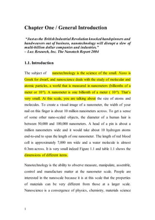
1. 1
Chapter One / General Introduction
“Justas the BritishIndustrial Revolution knocked handspinners and
handweavers out of business, nanotechnology will disrupt a slew of
multi-billion dollar companies and industries.”
– Lux Research, Inc. The Nanotech Report 2004
1.1. Introduction
The subject of nanotechnology is the science of the small. Nano is
Greek for dwarf, and nanoscience deals with the study of molecular and
atomic particles, a world that is measured in nanometers (billionths of a
meter or 10-9). A nanometer is one billionth of a meter ( 10-9). That’s
very small. At this scale, you are talking about the size of atoms and
molecules. To create a visual image of a nanometer, the width of your
nail on this finger is about 10 million nanometers across. To get a sense
of some other nano-scaled objects, the diameter of a human hair is
between 50,000 and 100,000 nanometers. A head of a pin is about a
million nanometers wide and it would take about 10 hydrogen atoms
end-to-end to span the length of one nanometer. The length of red blood
cell is approximately 7,000 nm wide and a water molecule is almost
0.3nm across. It is very small indeed Figure 1.1 and table 1.1 shows the
dimensions of different items.
Nanotechnology is the ability to observe measure, manipulate, assemble,
control and manufacture matter at the nanometer scale. People are
interested in the nanoscale because it is at this scale that the properties
of materials can be very different from those at a larger scale.
Nanoscience is a convergence of physics, chemistry, materials science
2. 2
and biology, which deals with the manipulation of materials at atomic,
molecular and macromolecular scales; nanotechnology is an emerging
engineering discipline that applies methods from nanoscience to create
products.
Figure 1.1 (a) Less than a nanometer, individual atoms is up to a few
angstroms, or up to a few tenths of a nanometer, in diameter.
(b) Nanometer, ten shoulder-to-shoulder hydrogen atoms. DNA
molecules are about 2.5 nanometers wide.
(c) A thousands of nanometers, biological cells, like these red blood
cells, have diameters in the range of thousands of nanometers.
Table 1.1 The dimension of some different items.
Dimensions (nm)
Items
1
Width of an Atom
2
The Width Across a DNA Molecule
5 – 50
Protein
75 – 100
Virus
800
The Width of a Dust Particle
1,000 – 10,000
Bacteria
10,000
White Blood Cell
100,000
The Width of a Hair
3. 3
or arrest the propagation of defects when the material is stressed, thus
giving it strength. If these grains can be made very small, or even
nanoscale in size, the interface area within the material greatly
increases, which enhances its strength. For example, nanocrystalline
nickel is as strong as hardened steel. Understanding surfaces and
interfaces is a key challenge for those working on nanomaterials, and
one where new imaging and analysis instruments are vital.