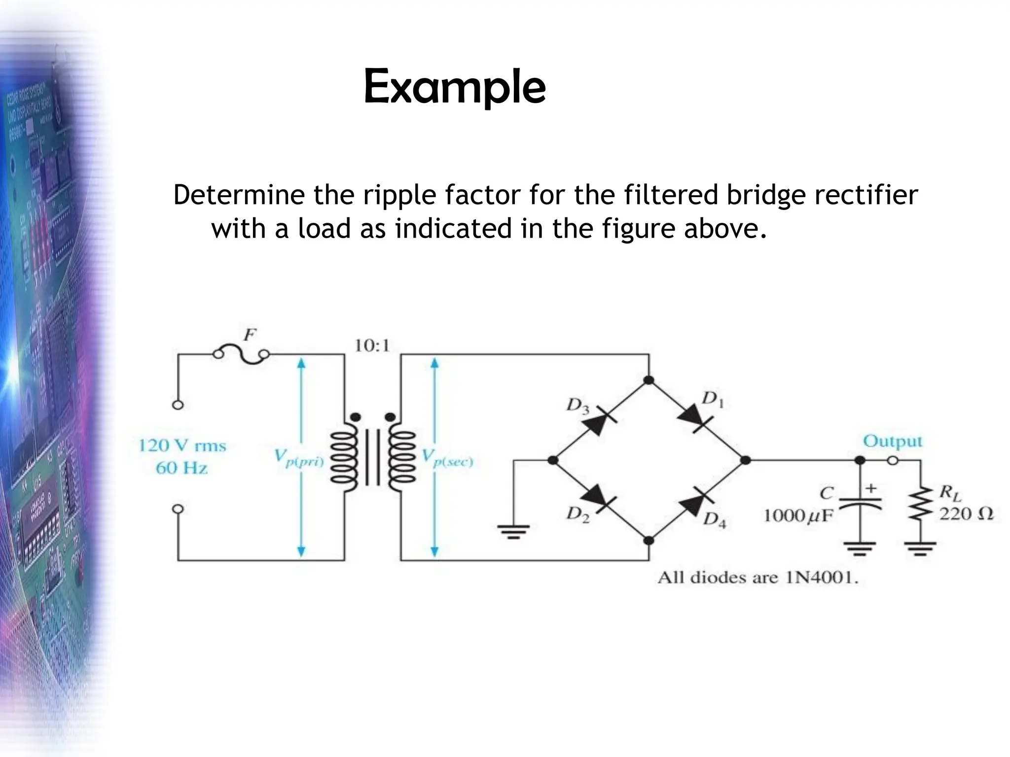
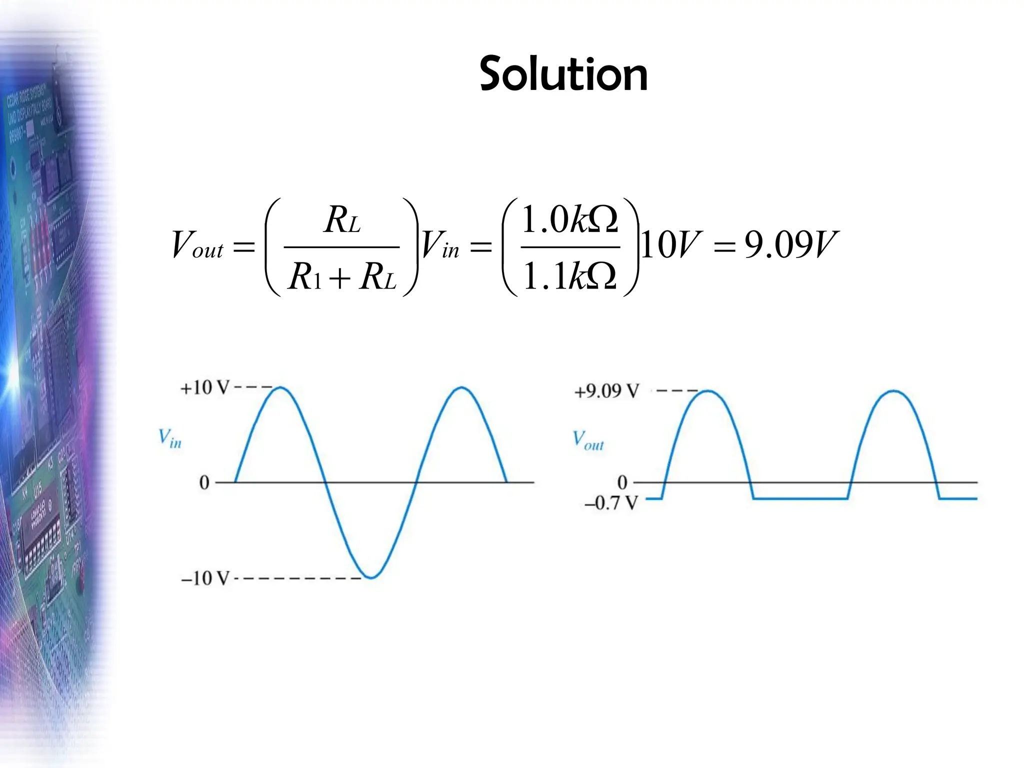
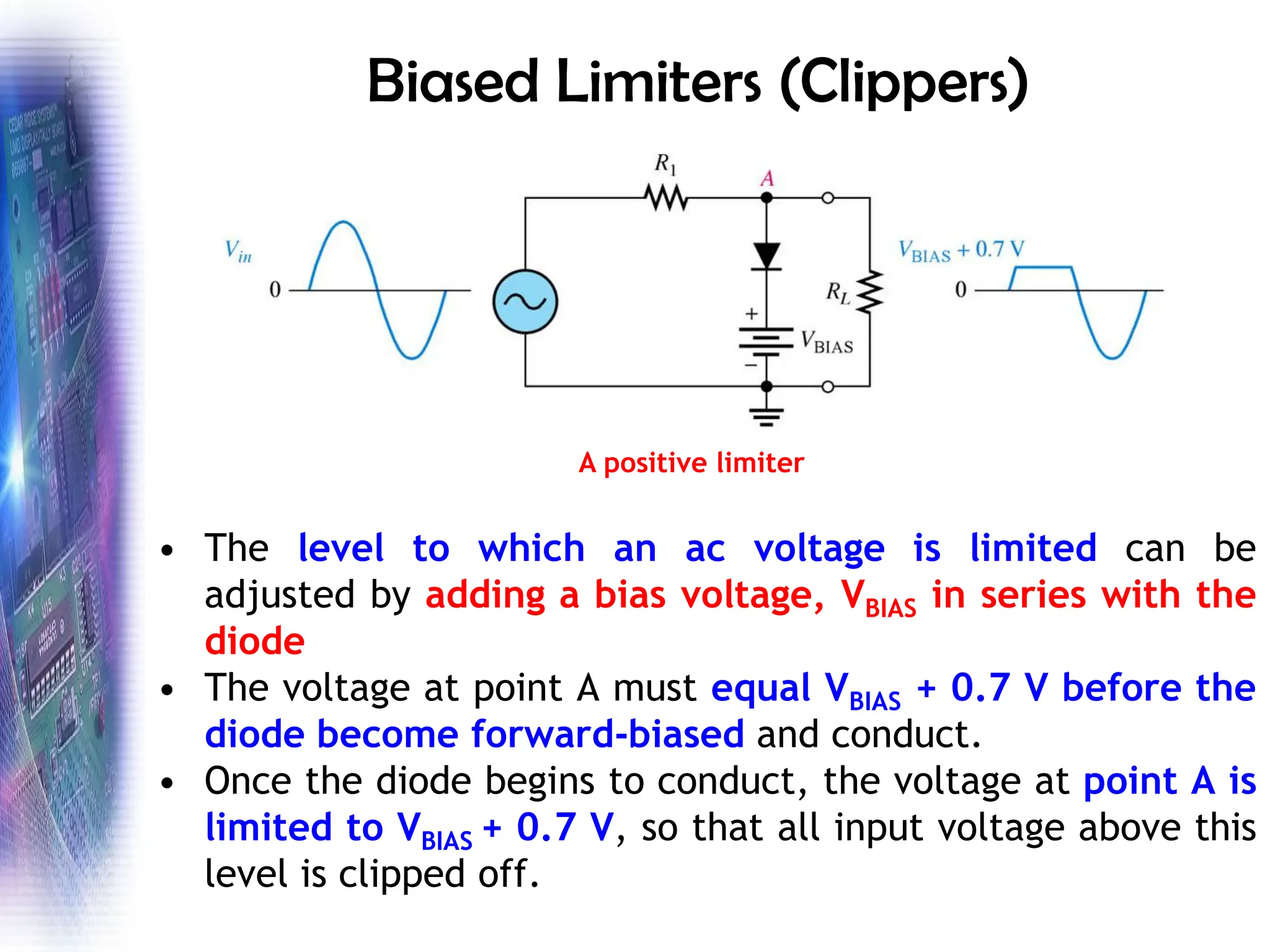
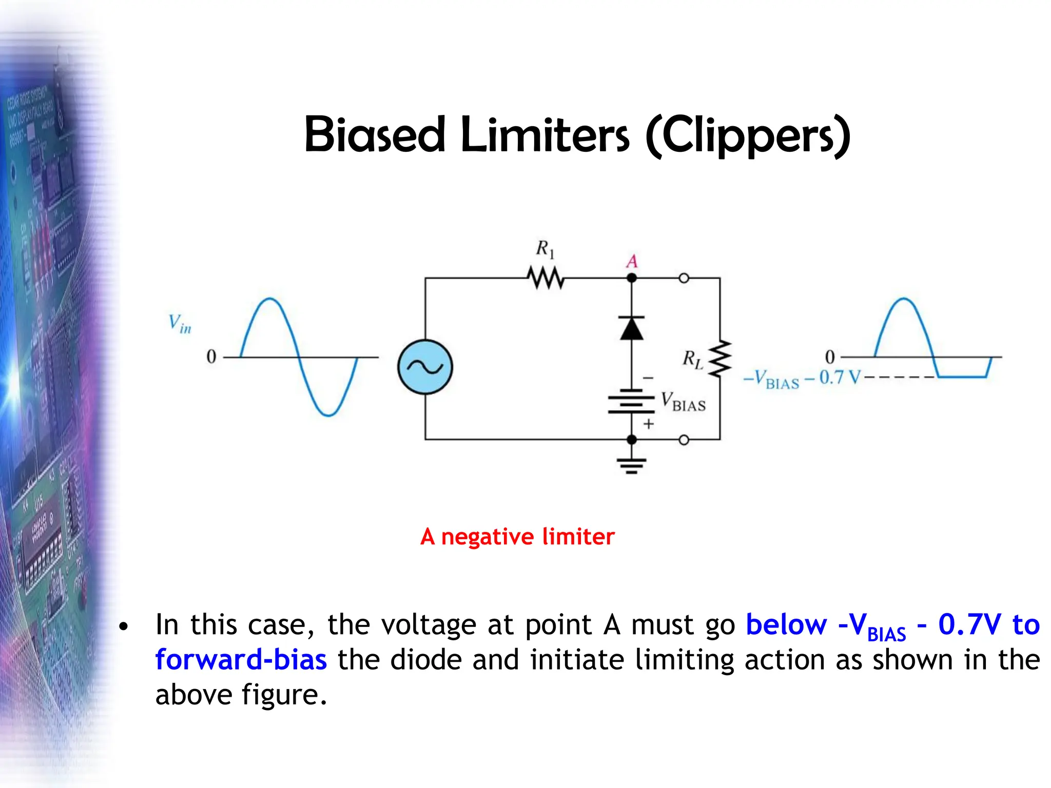
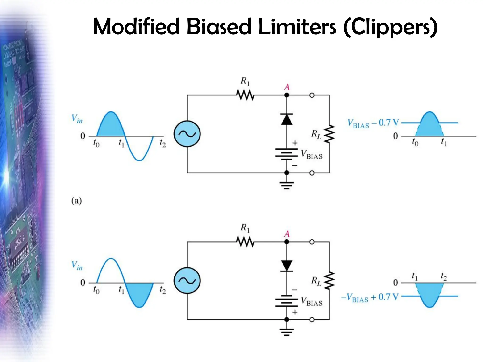
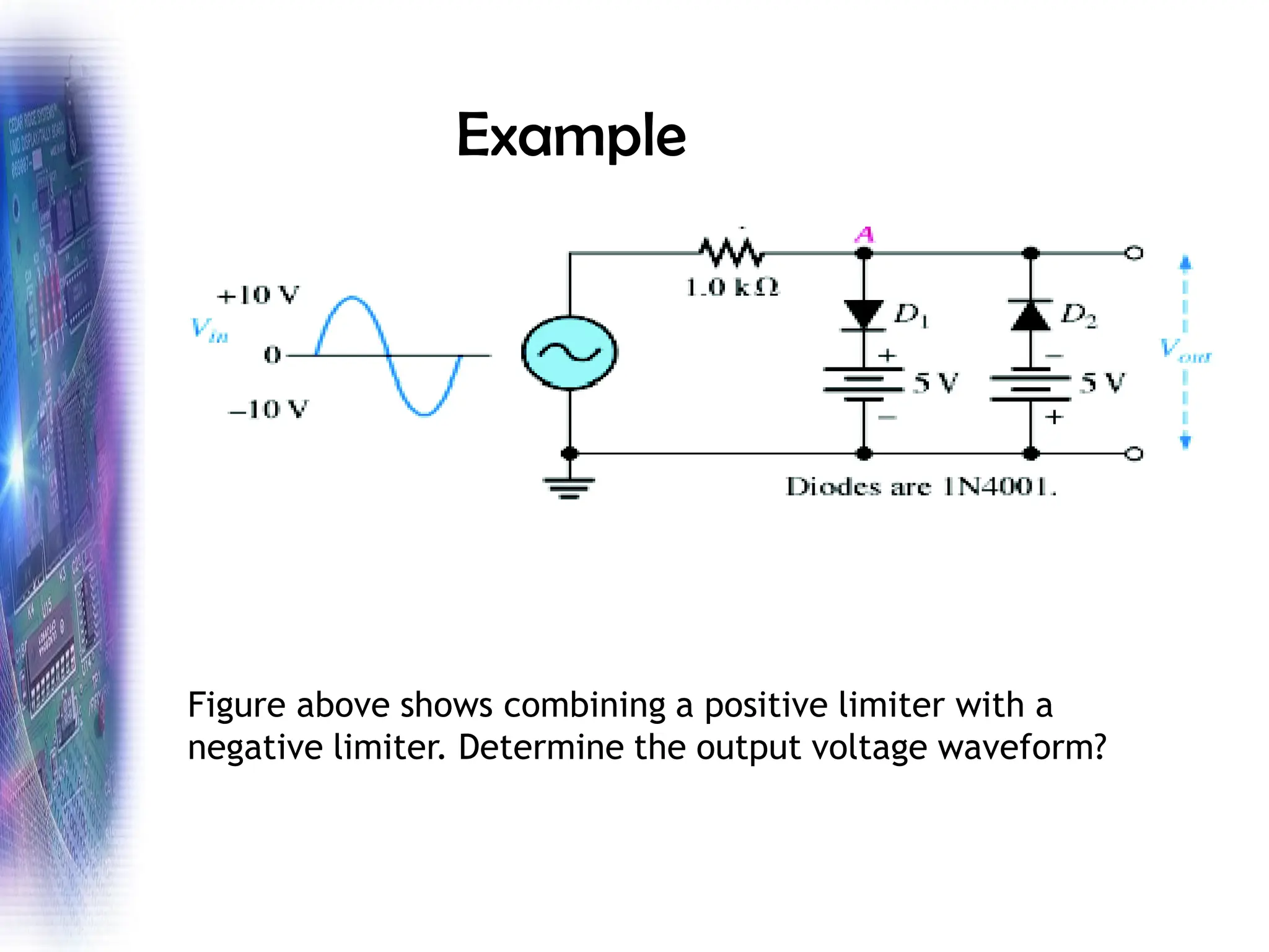
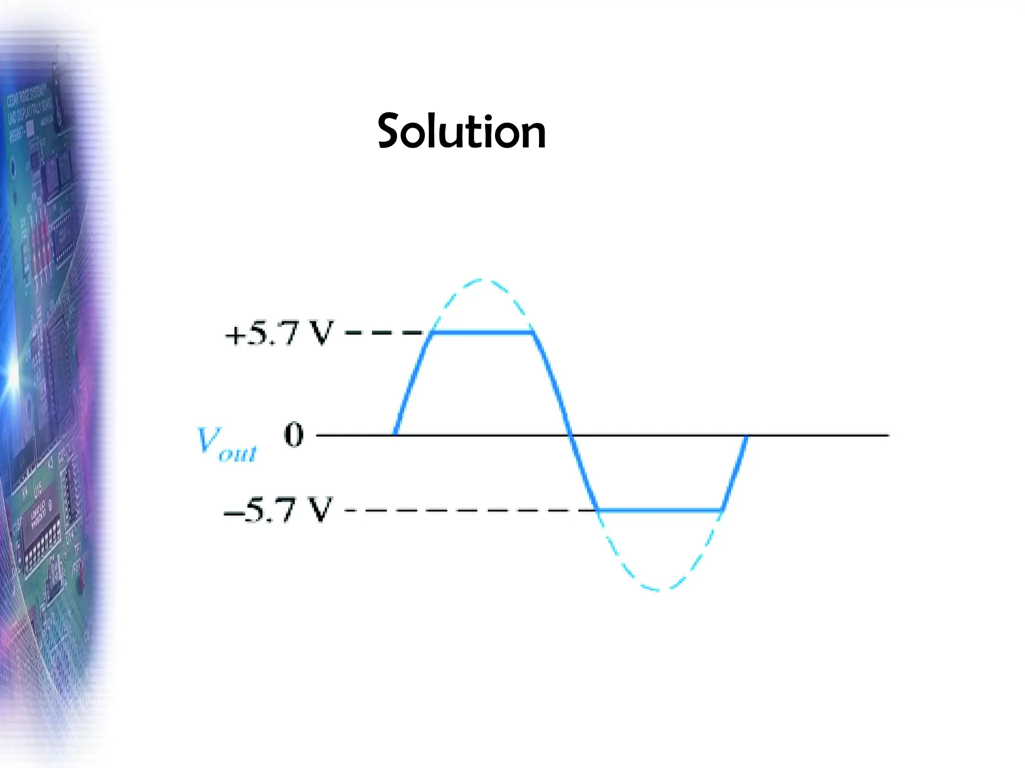
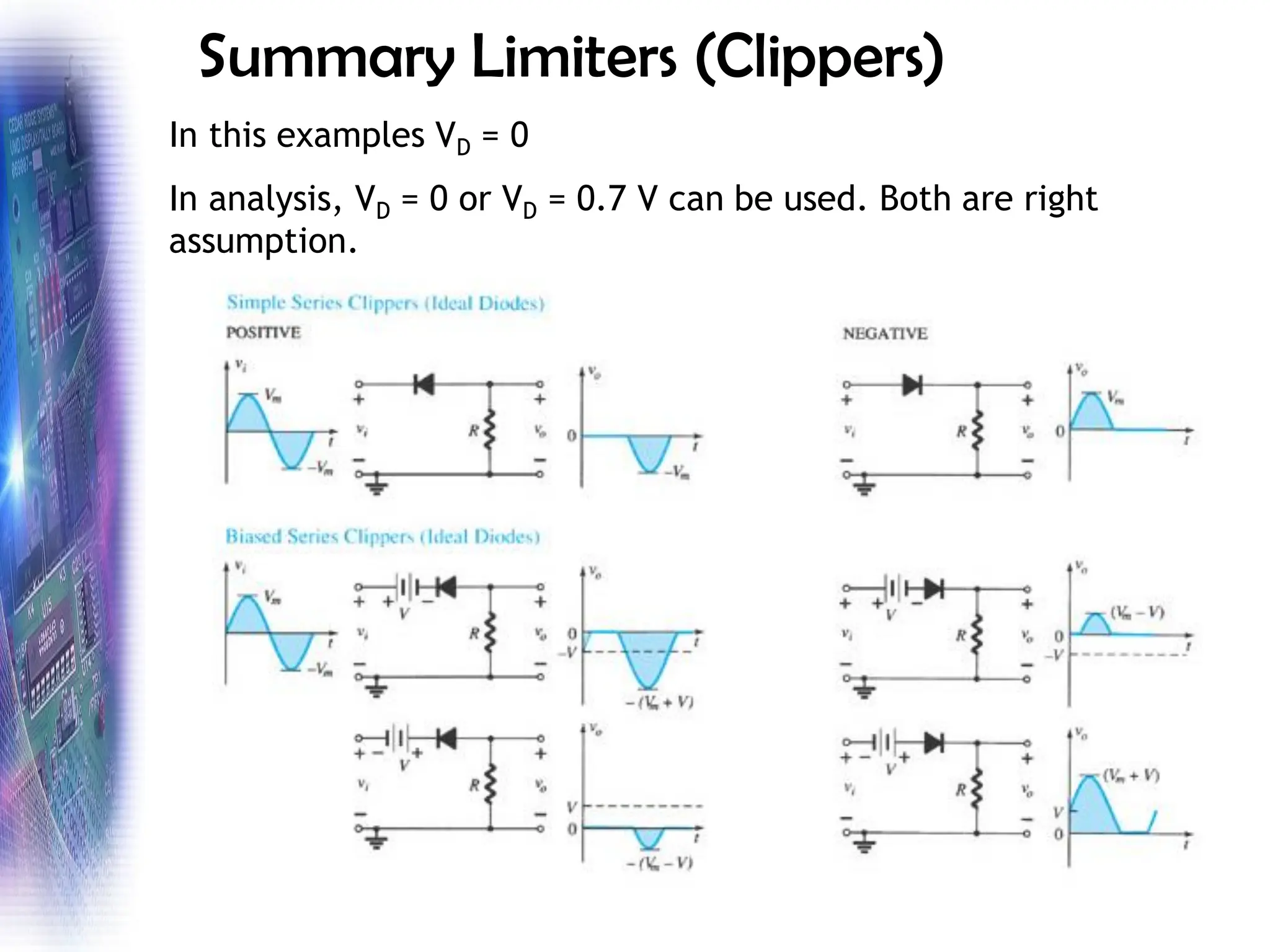
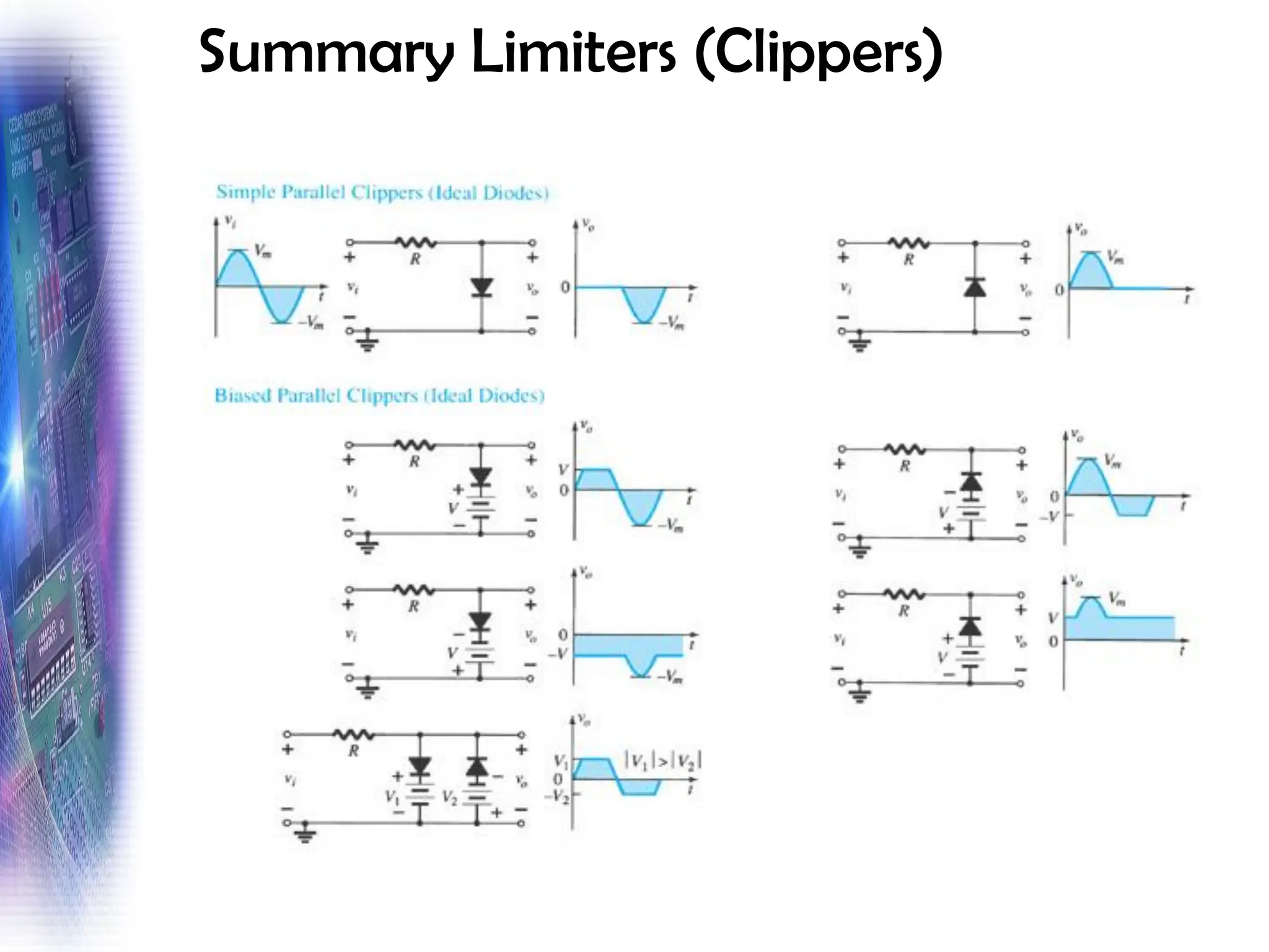
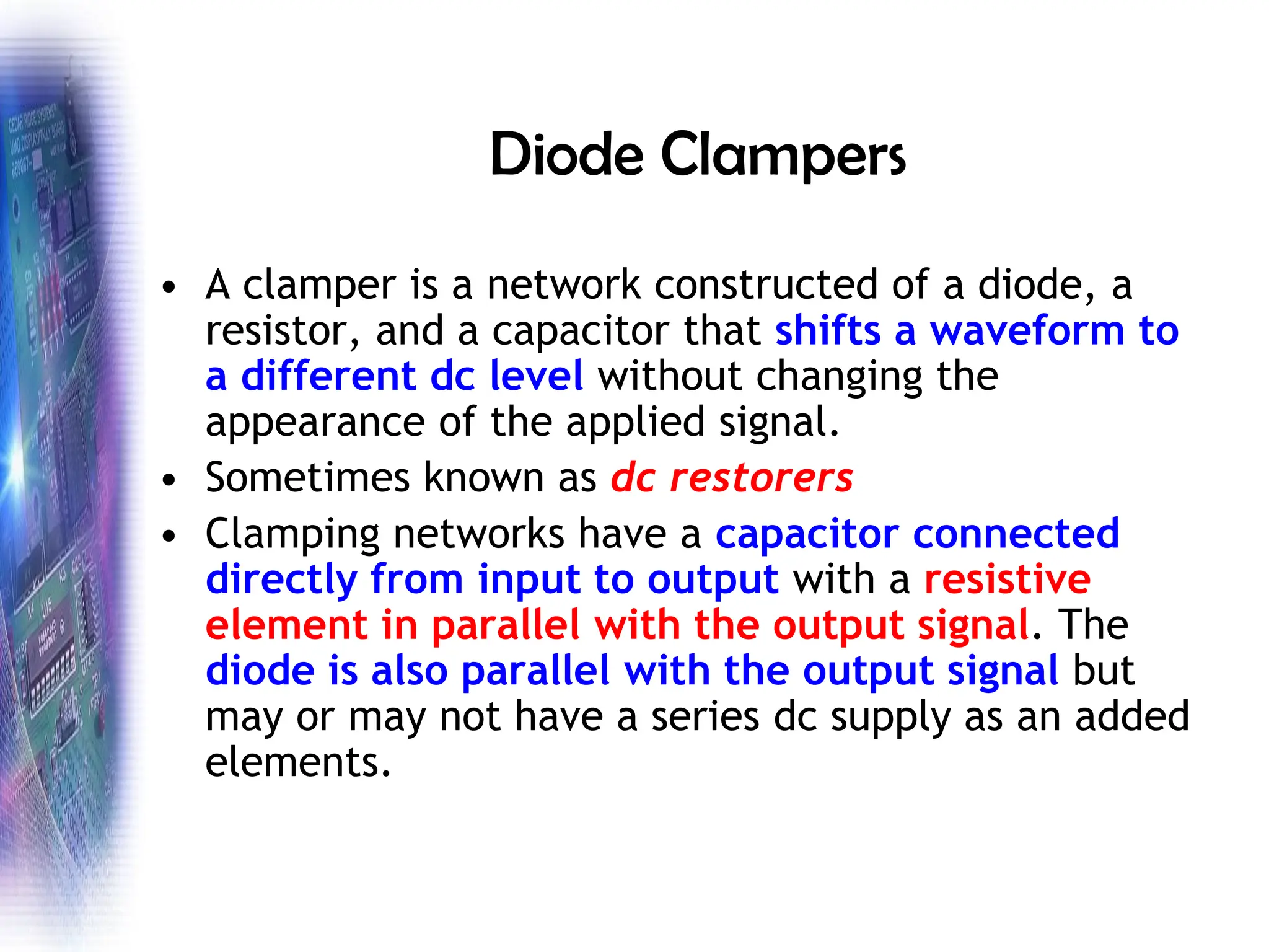
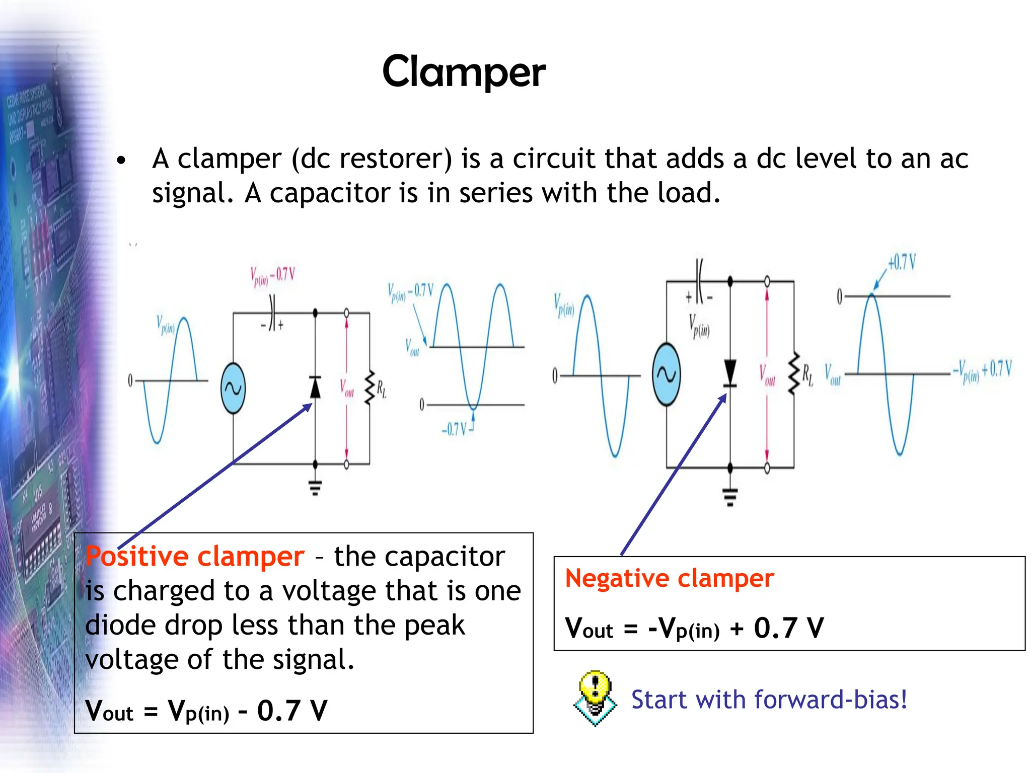
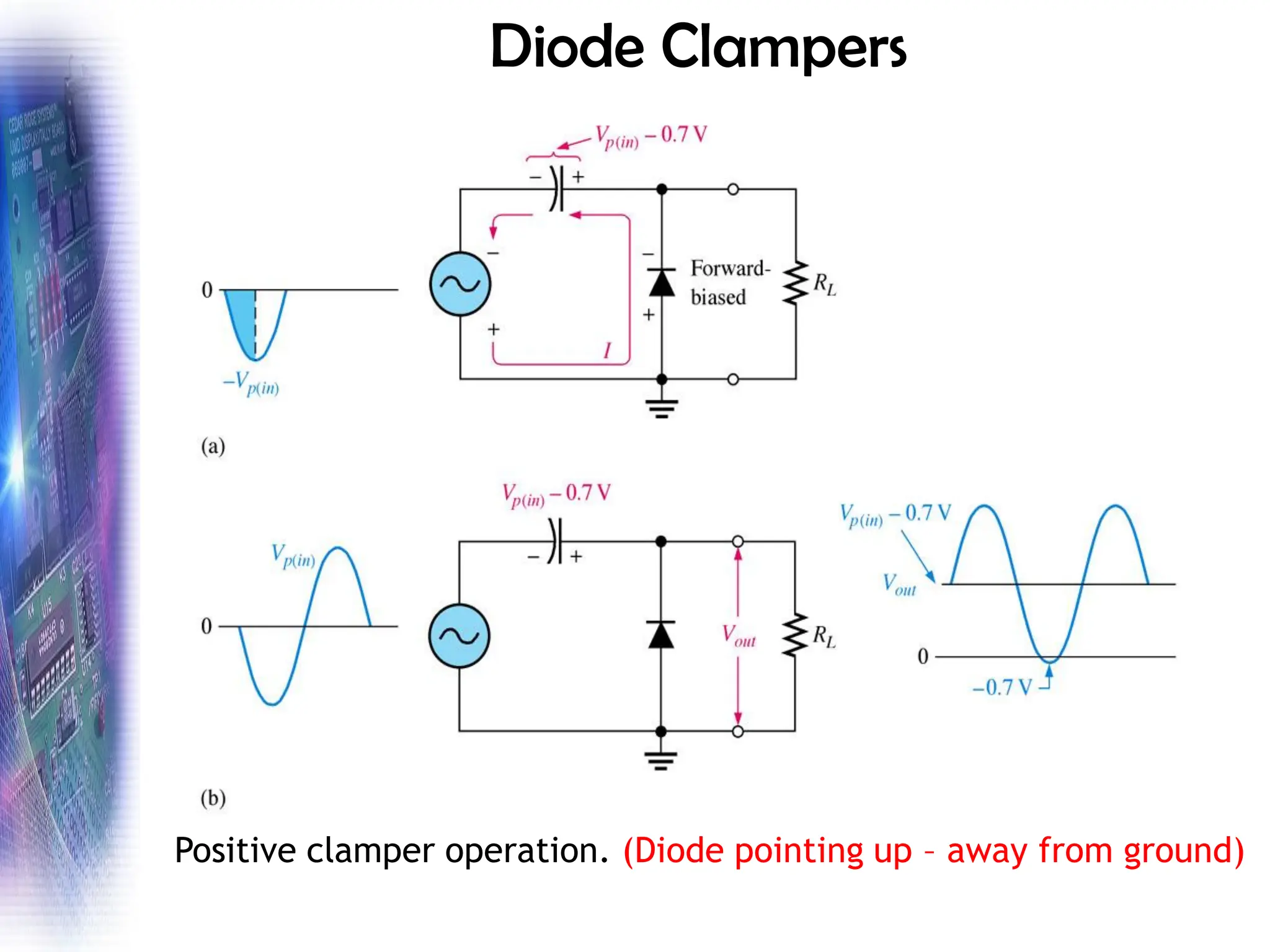
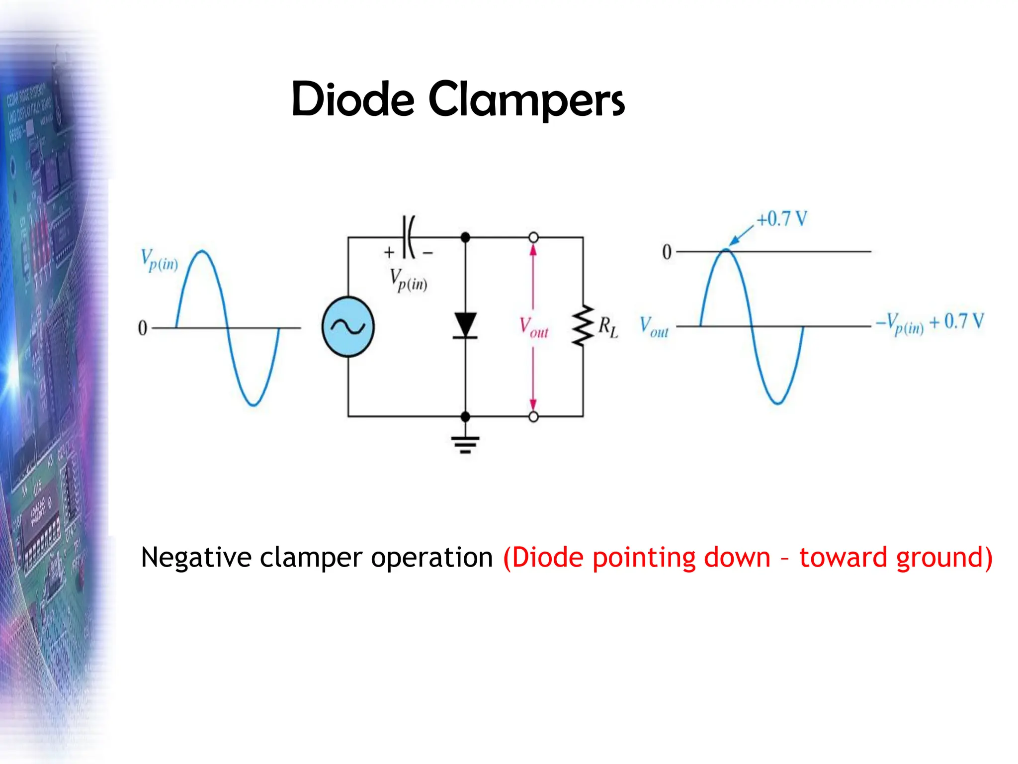
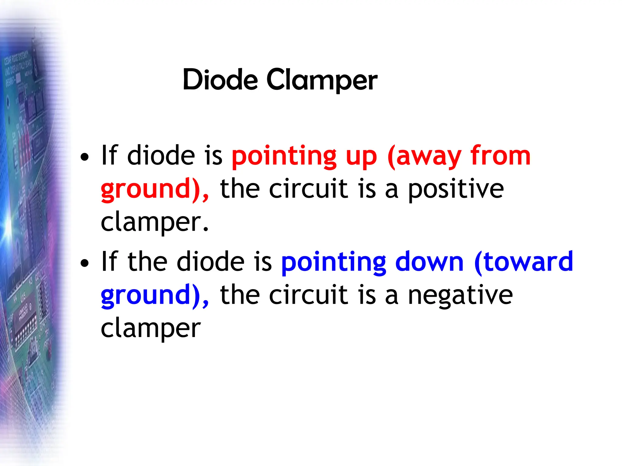
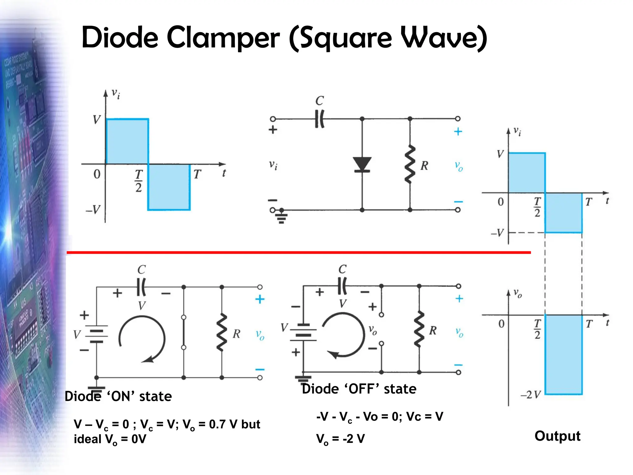
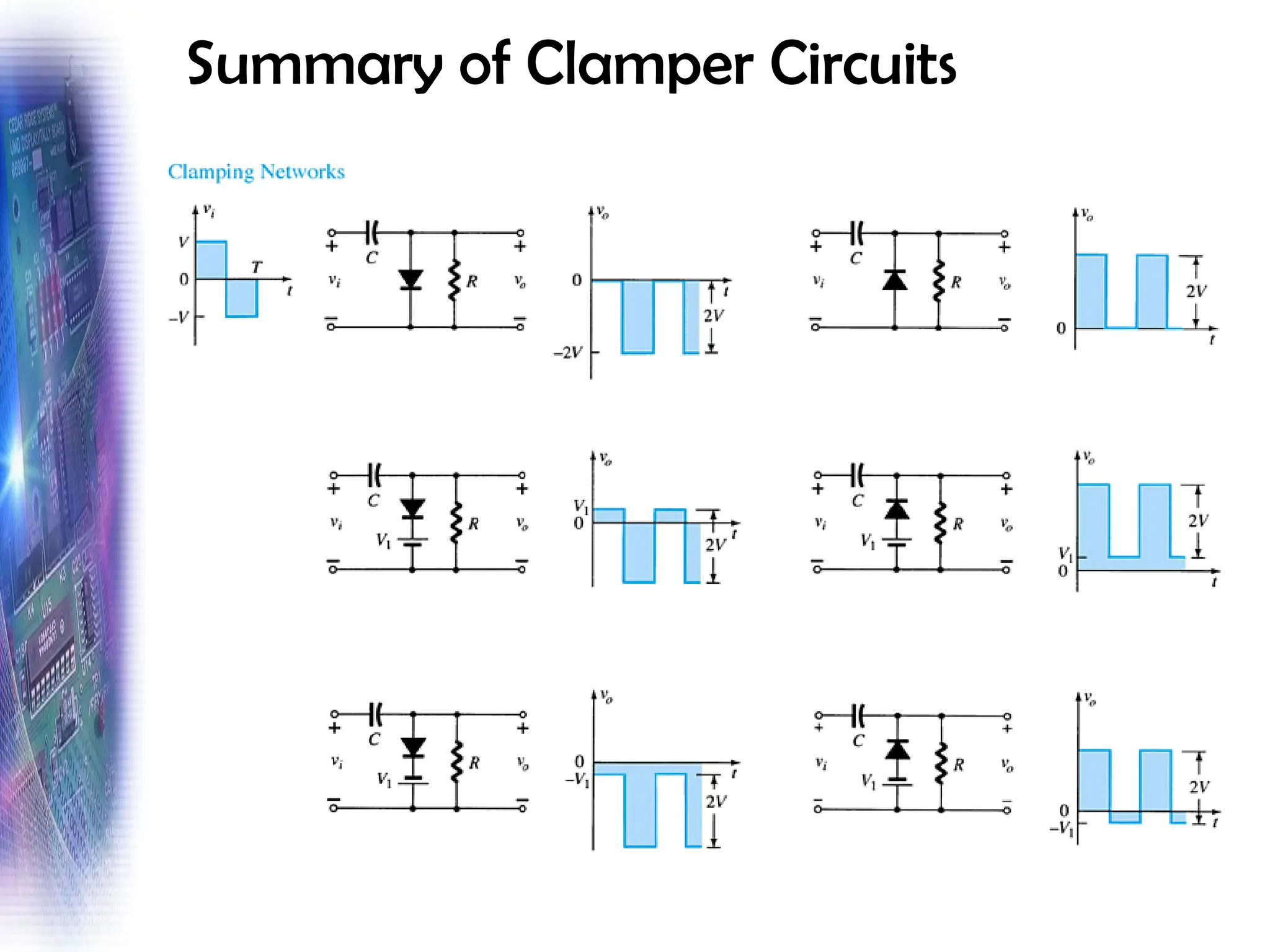
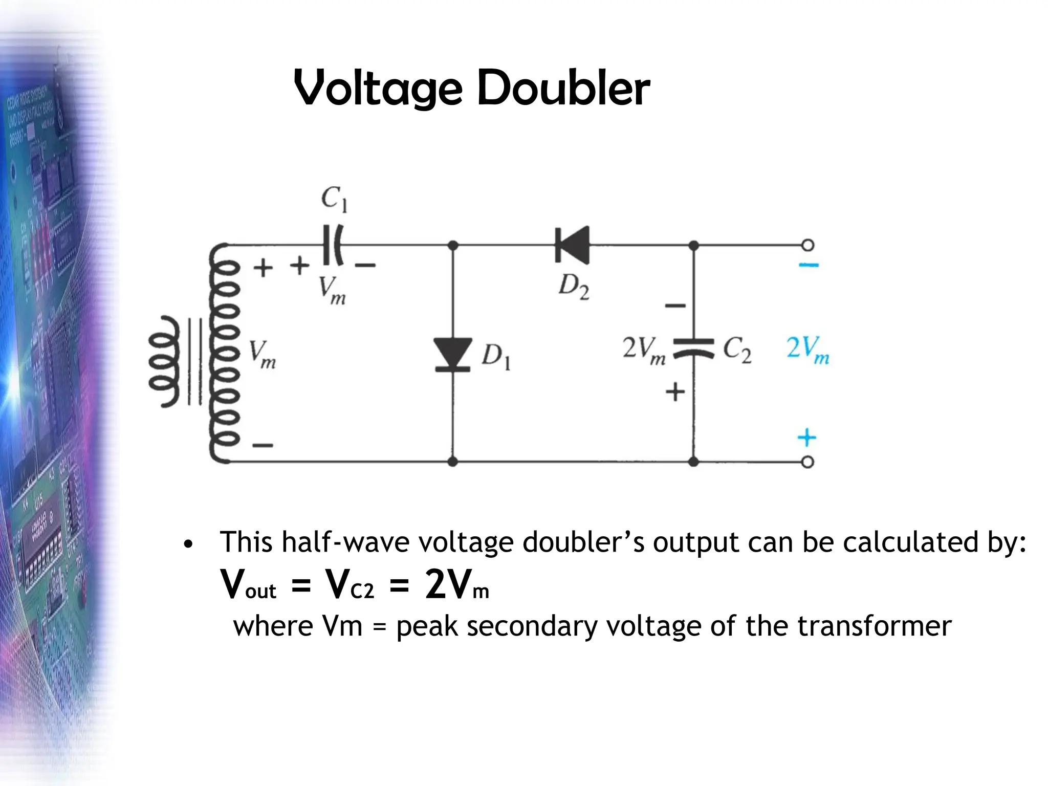
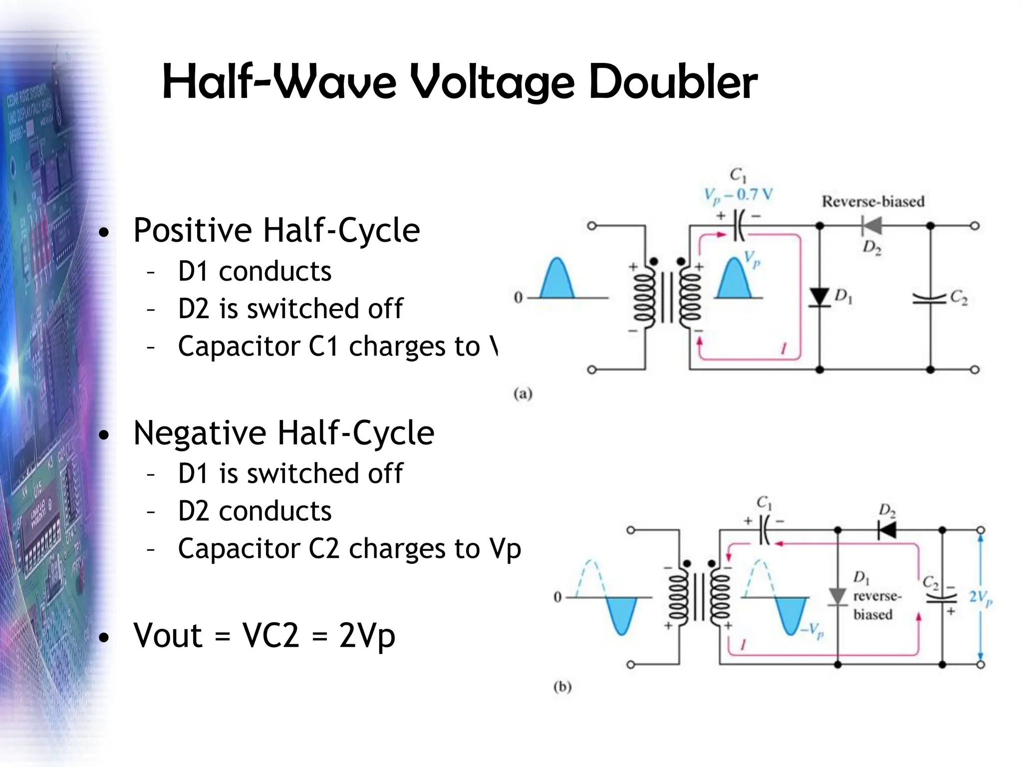
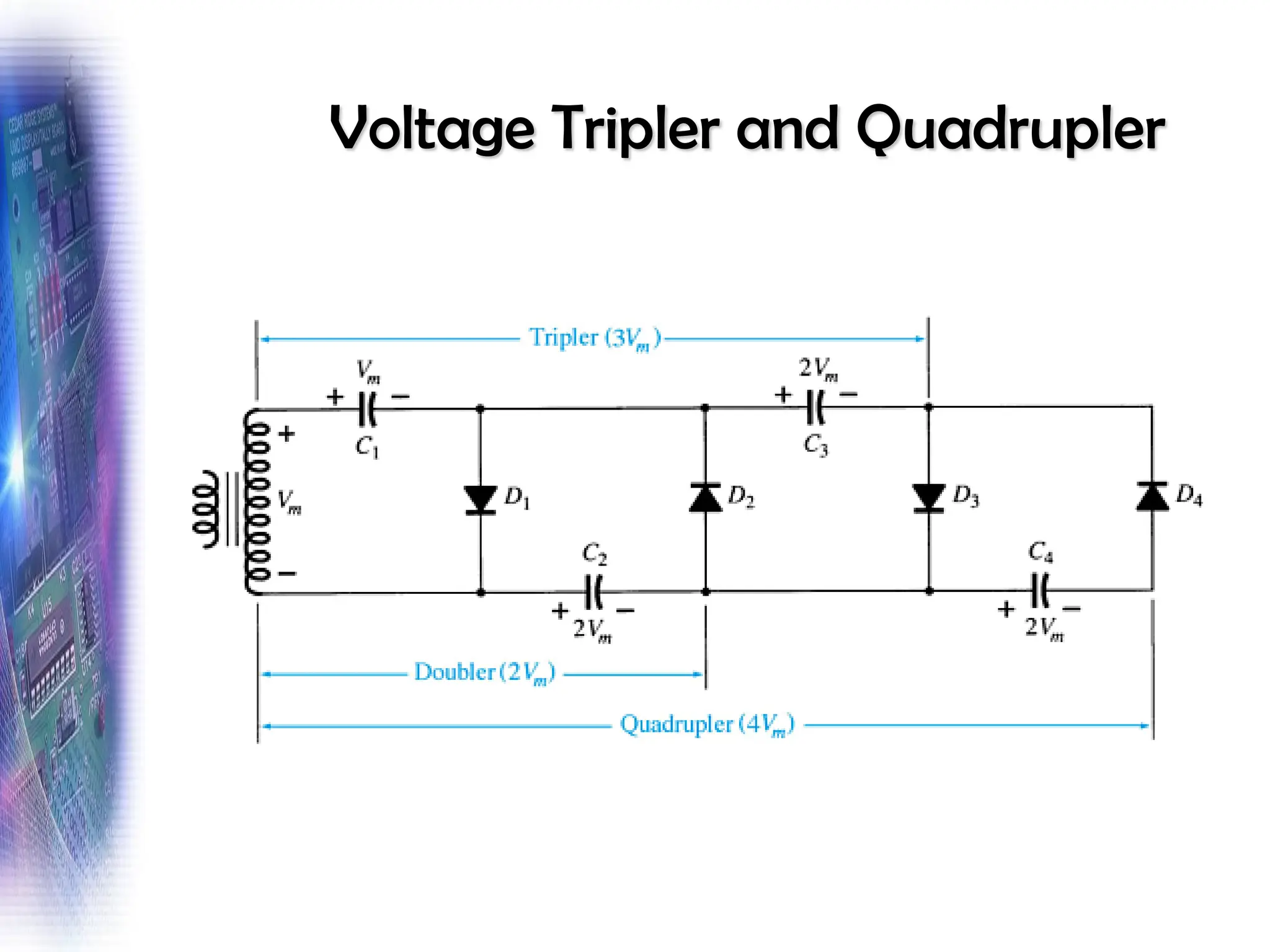
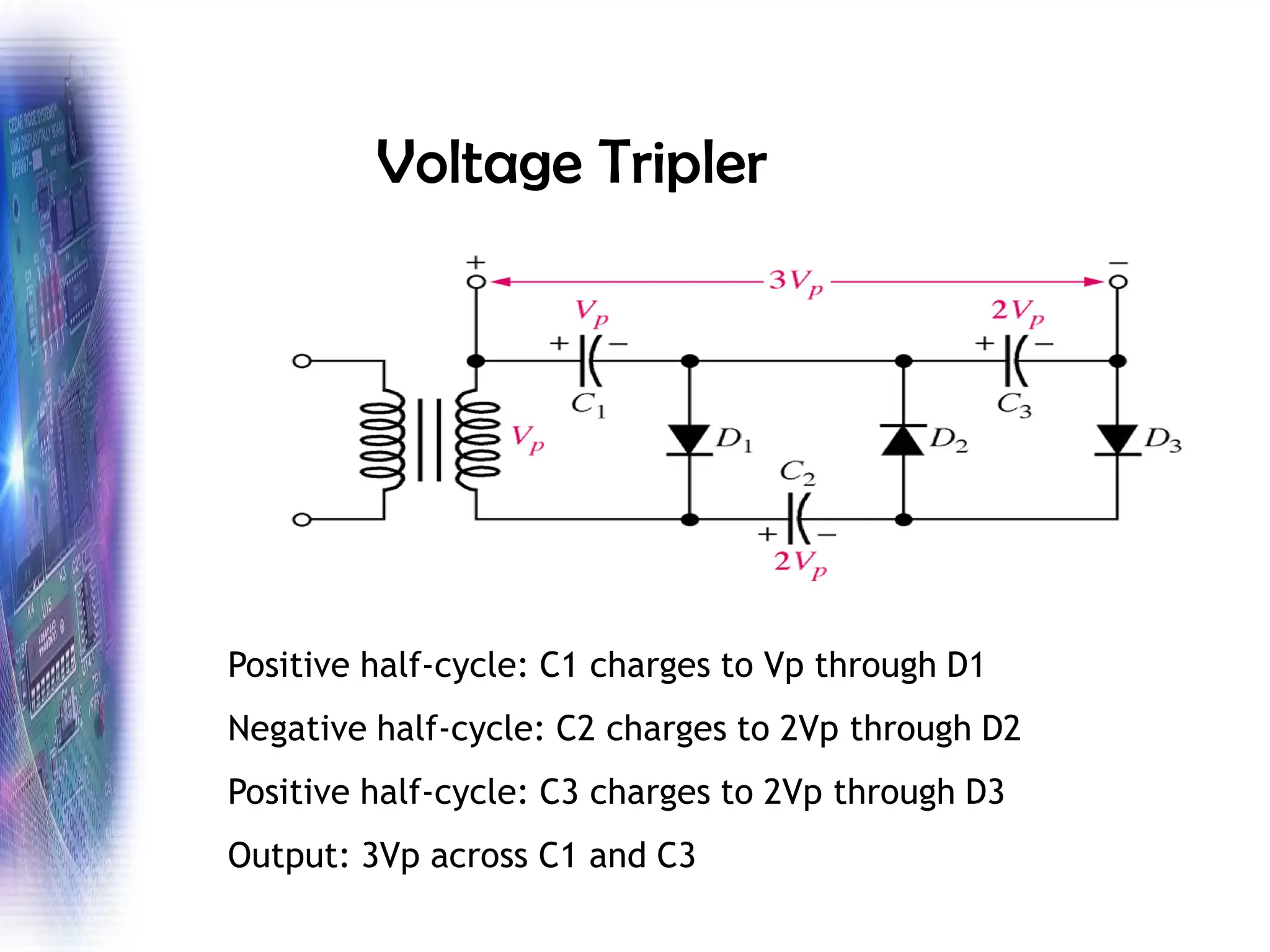
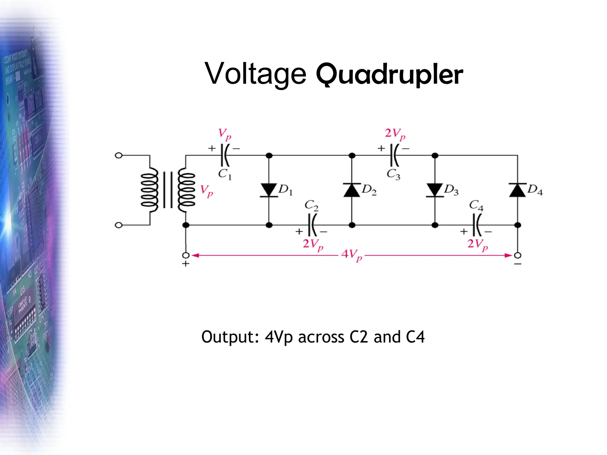
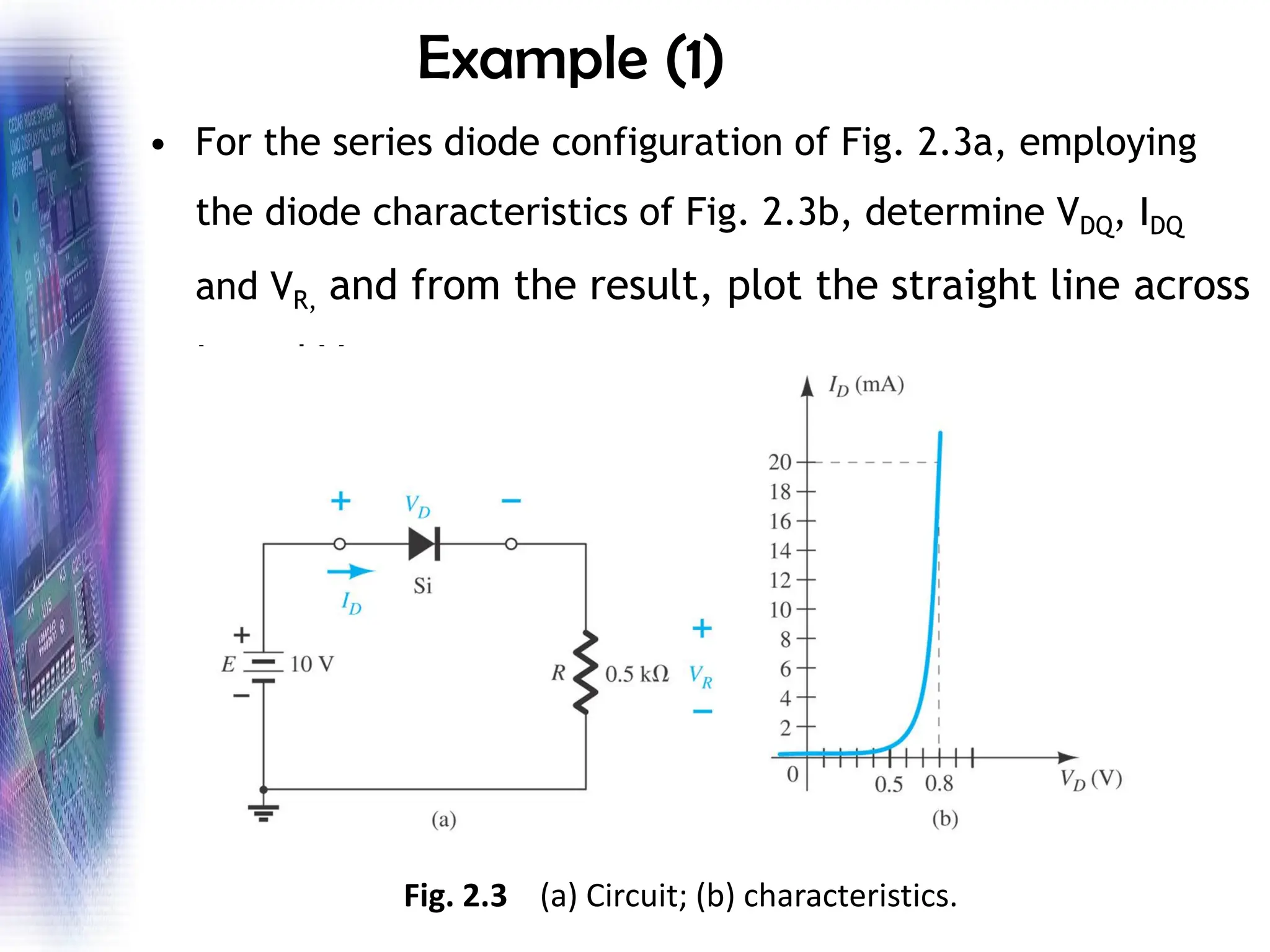
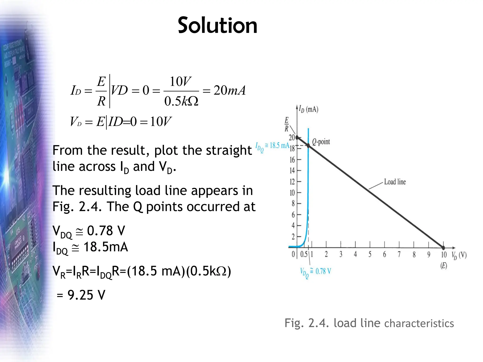
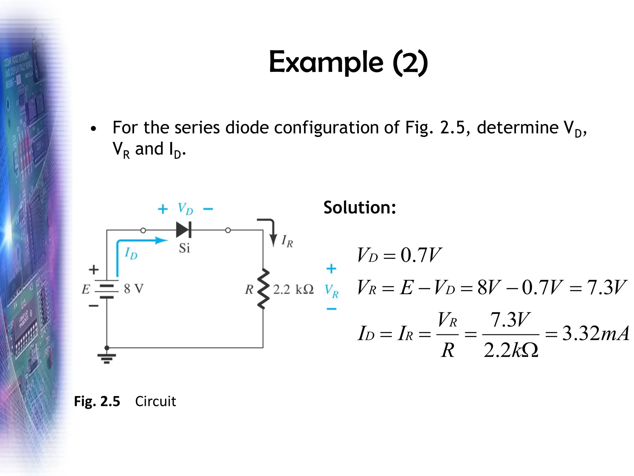
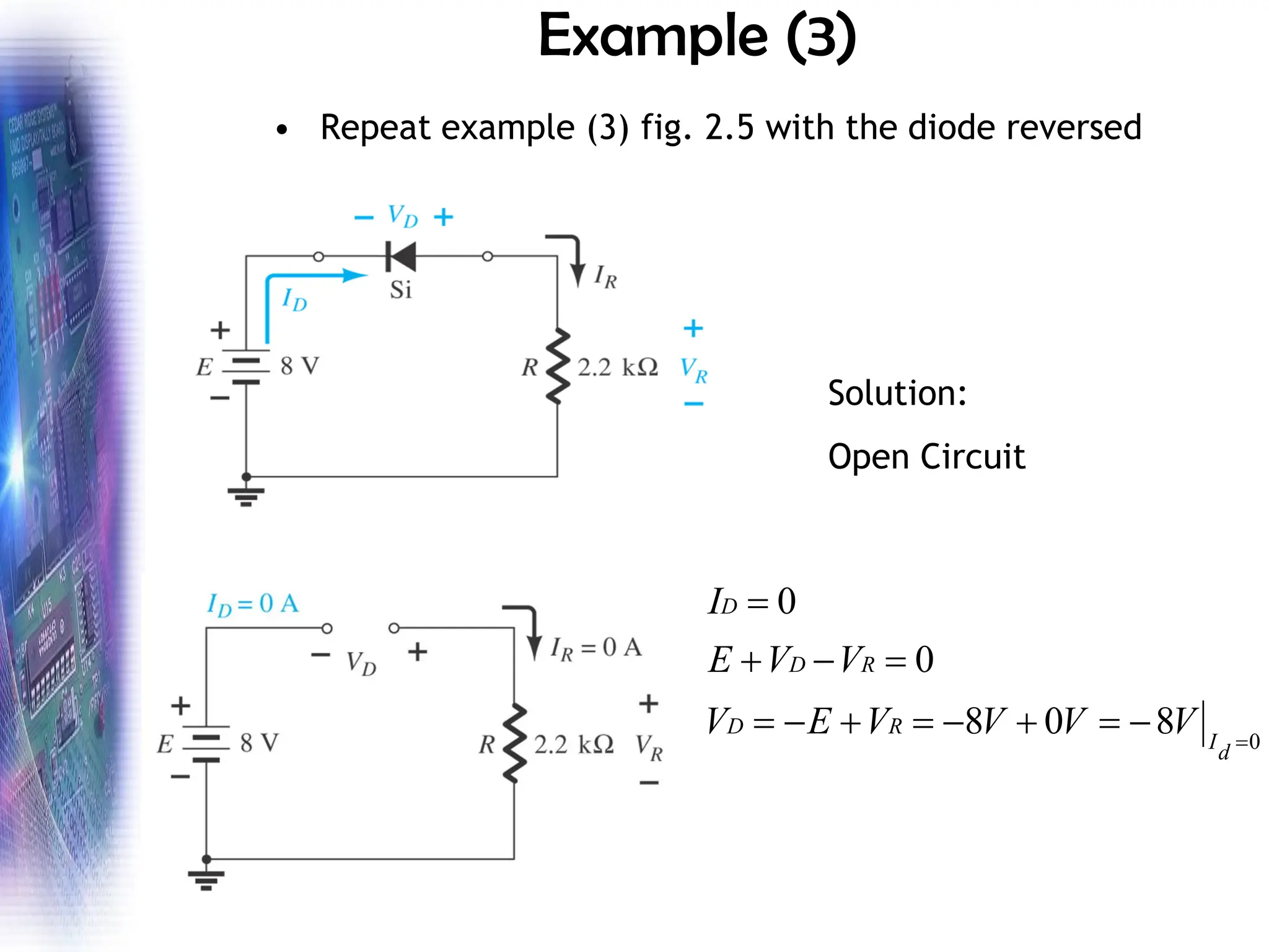
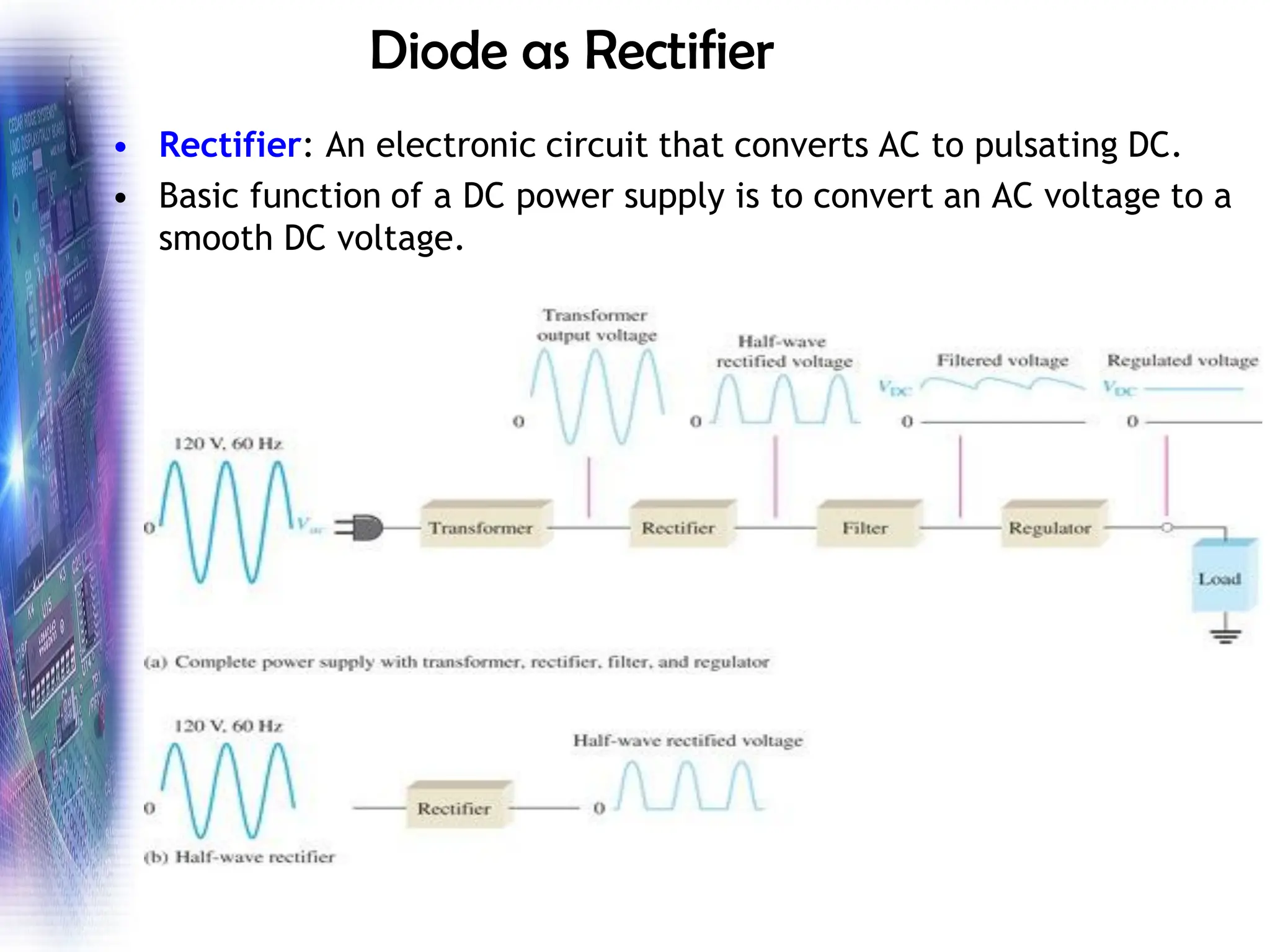
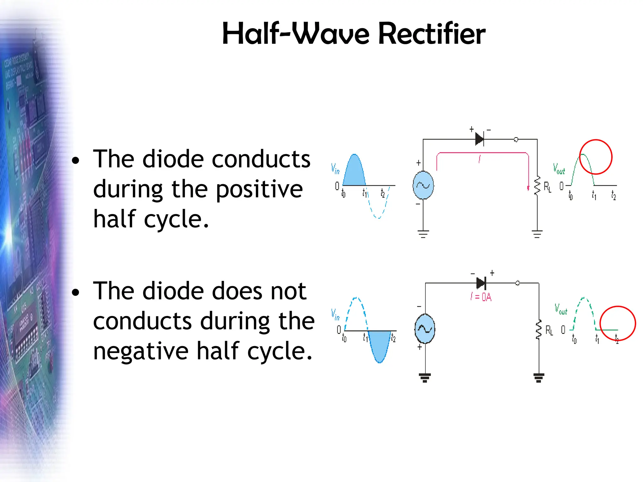
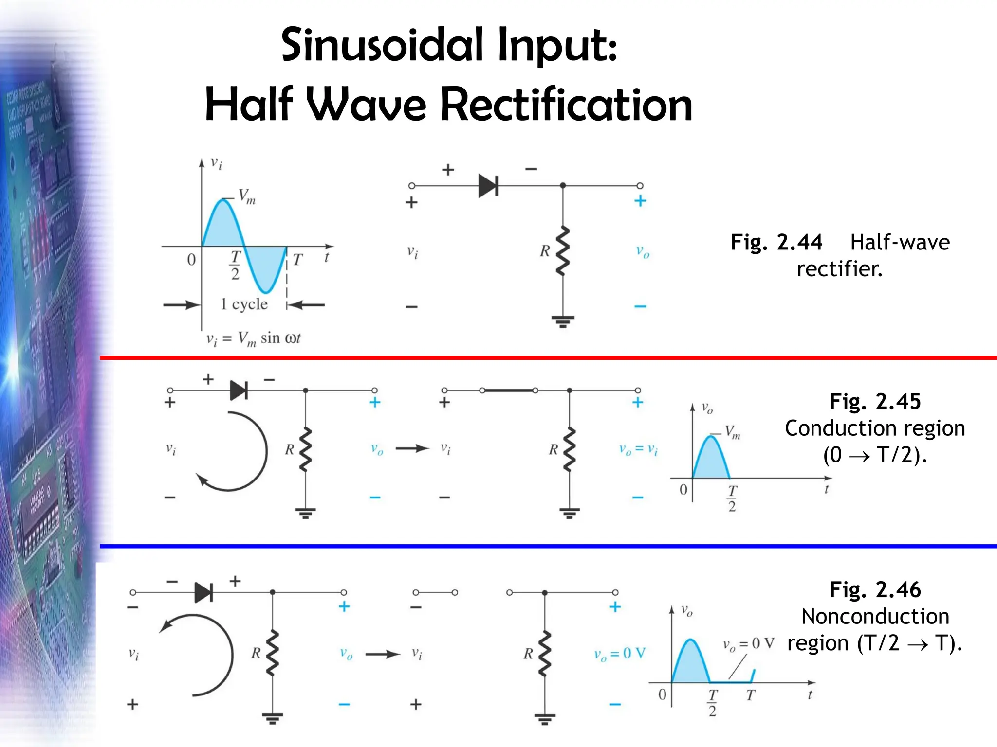
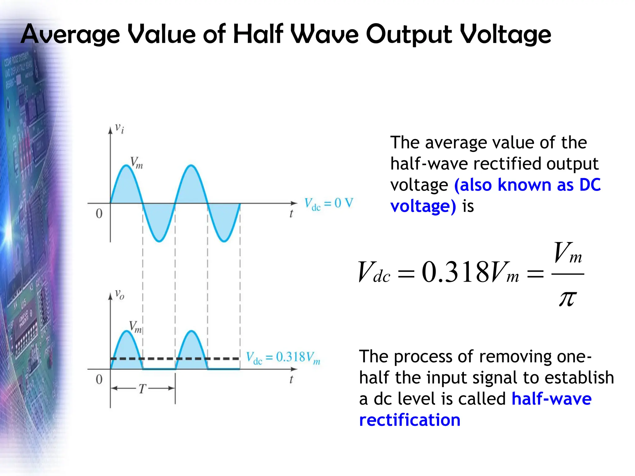
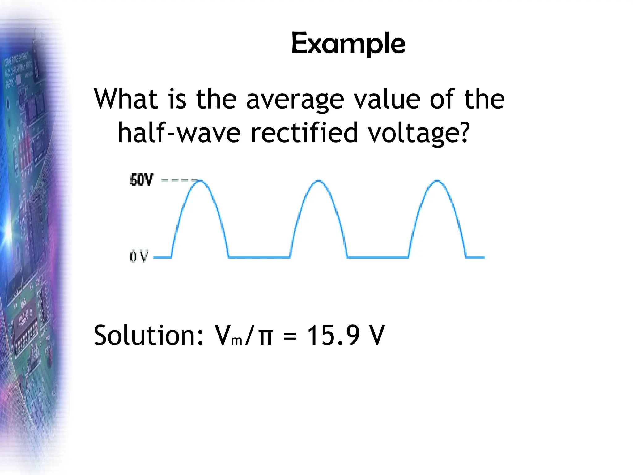
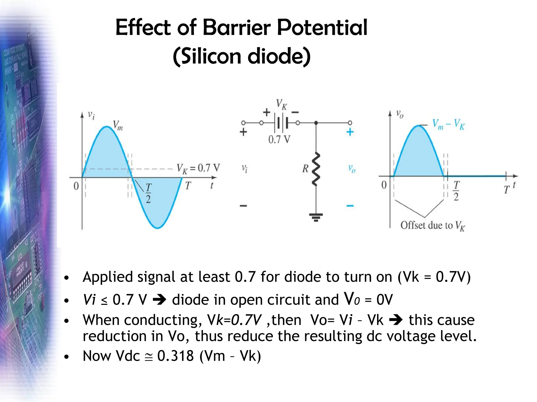
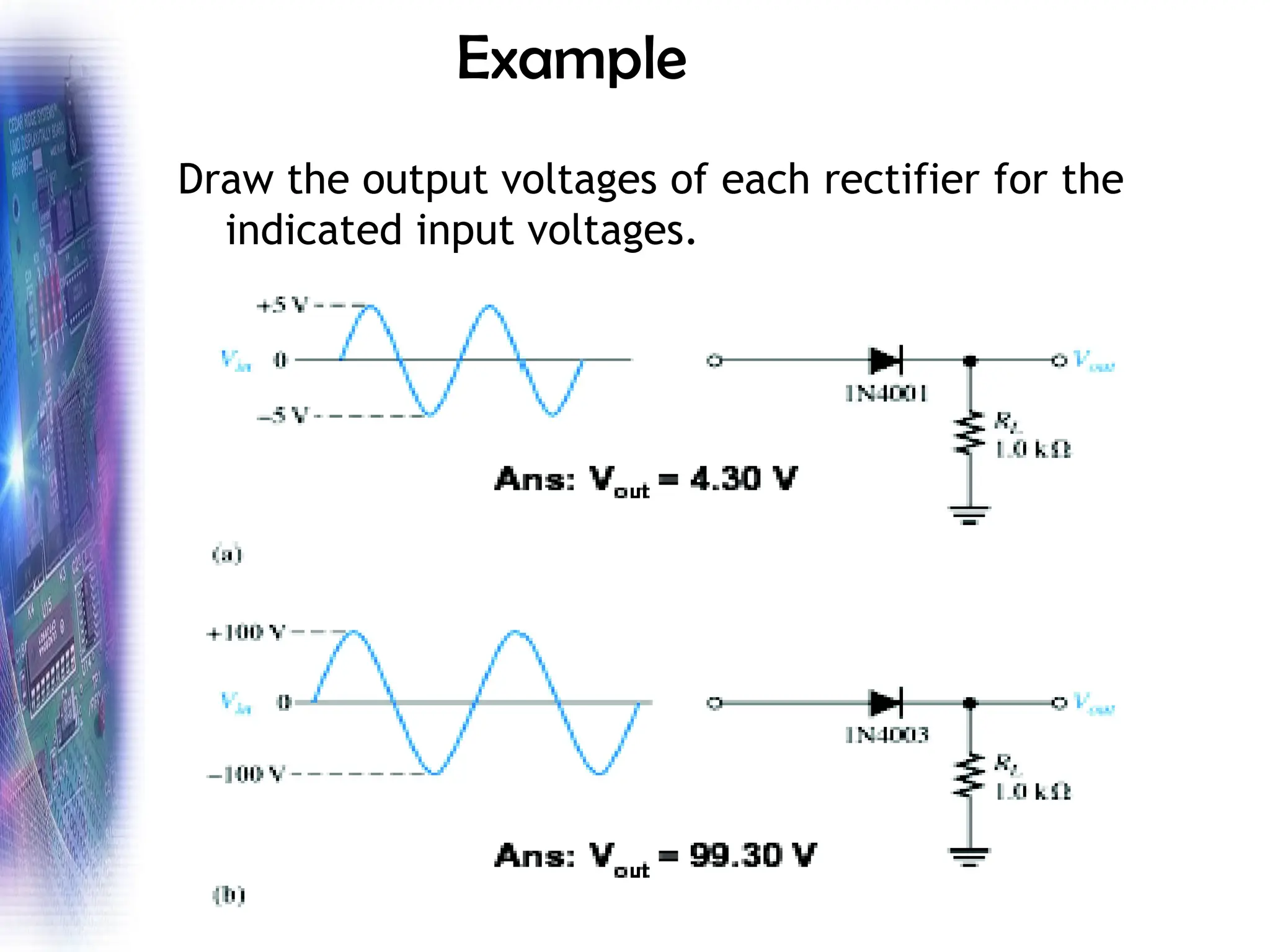
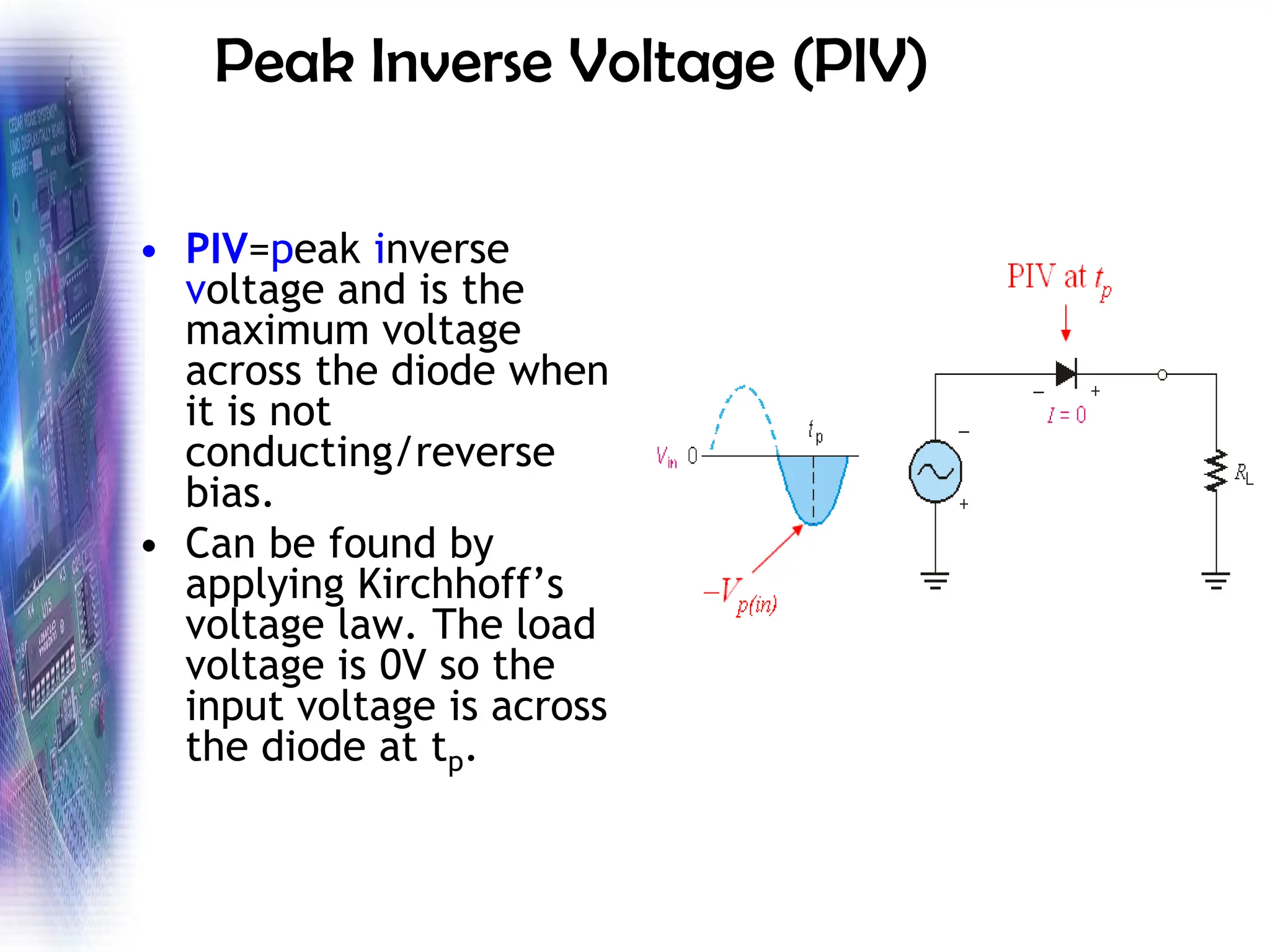
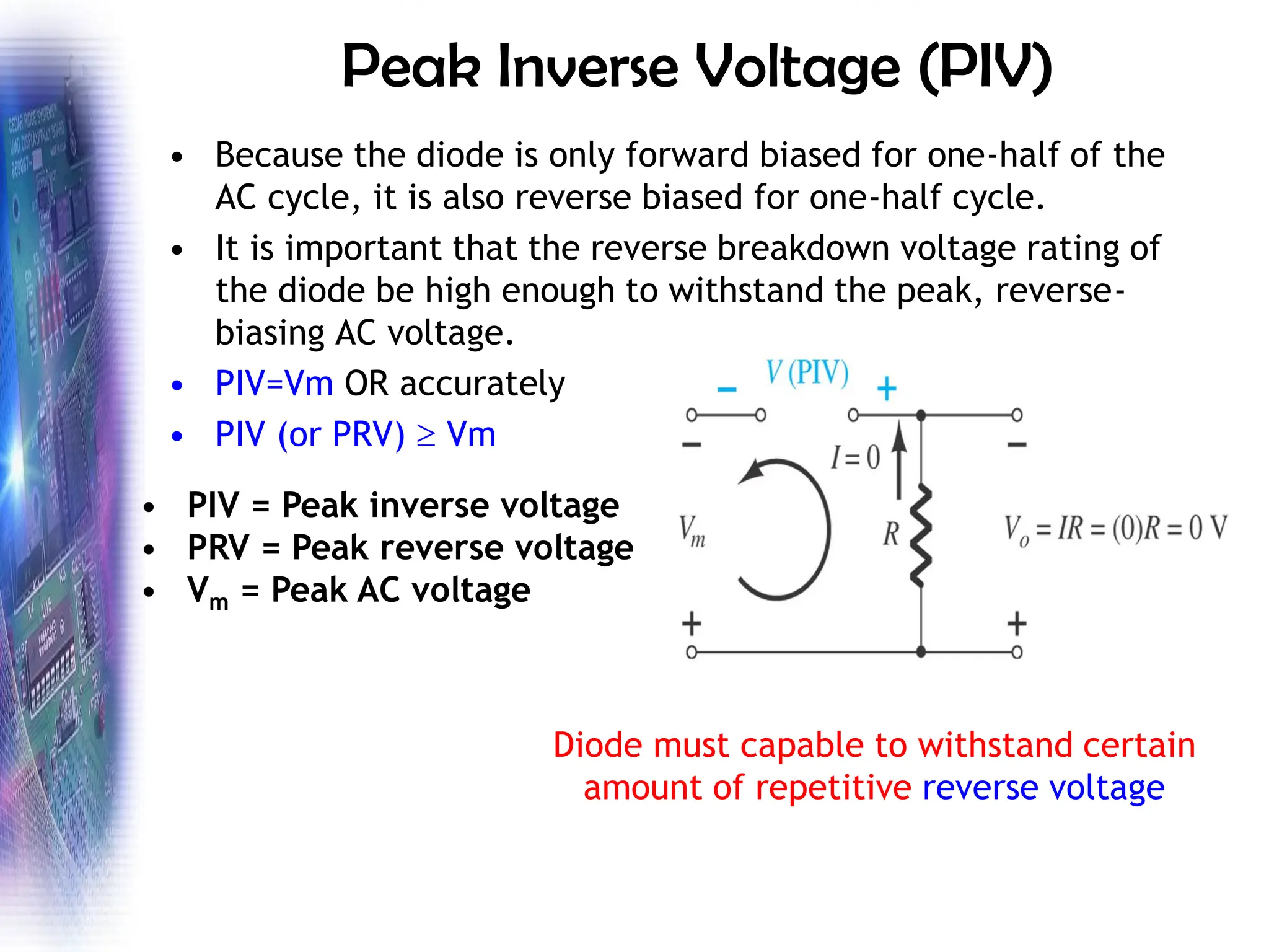
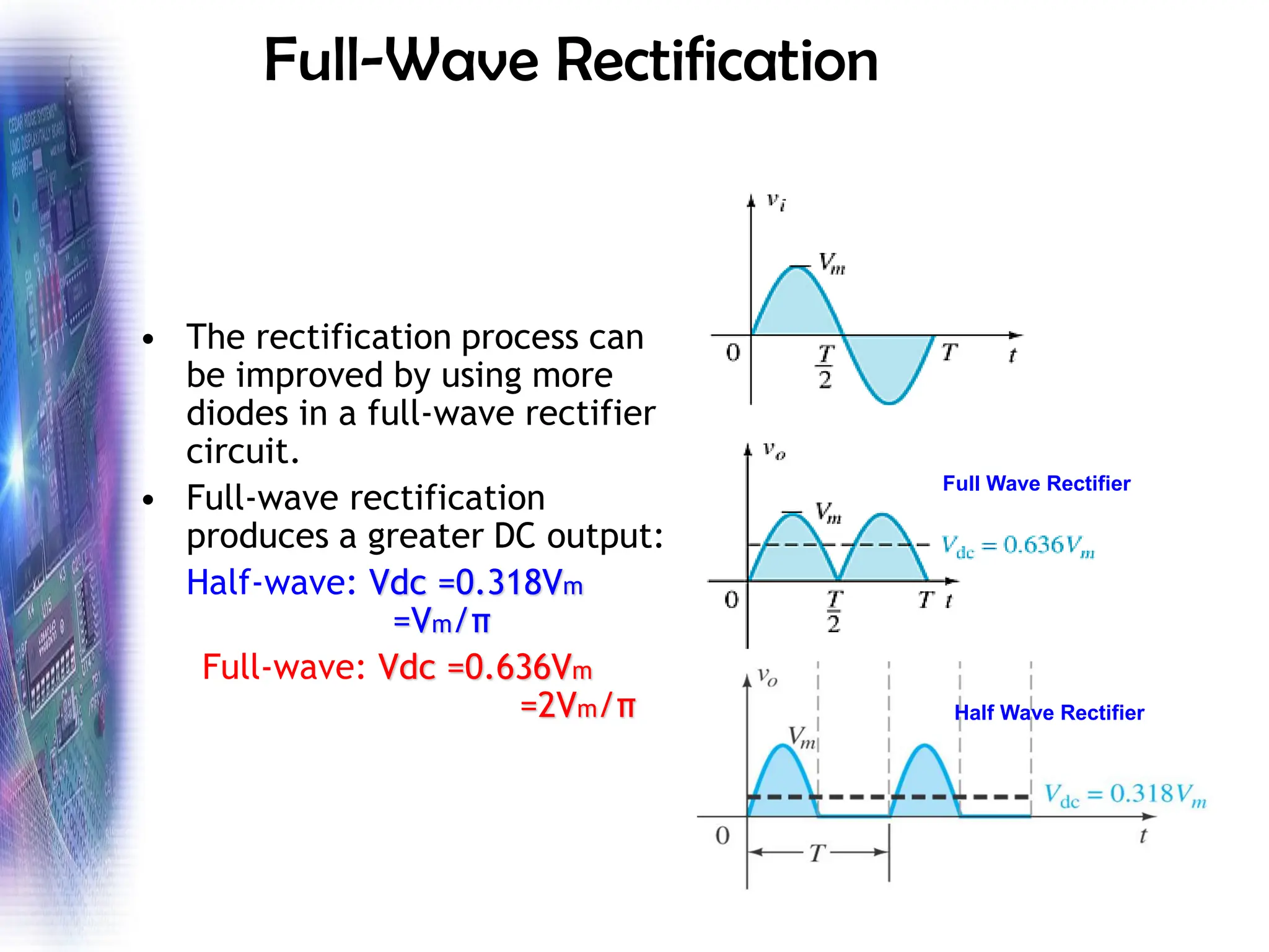
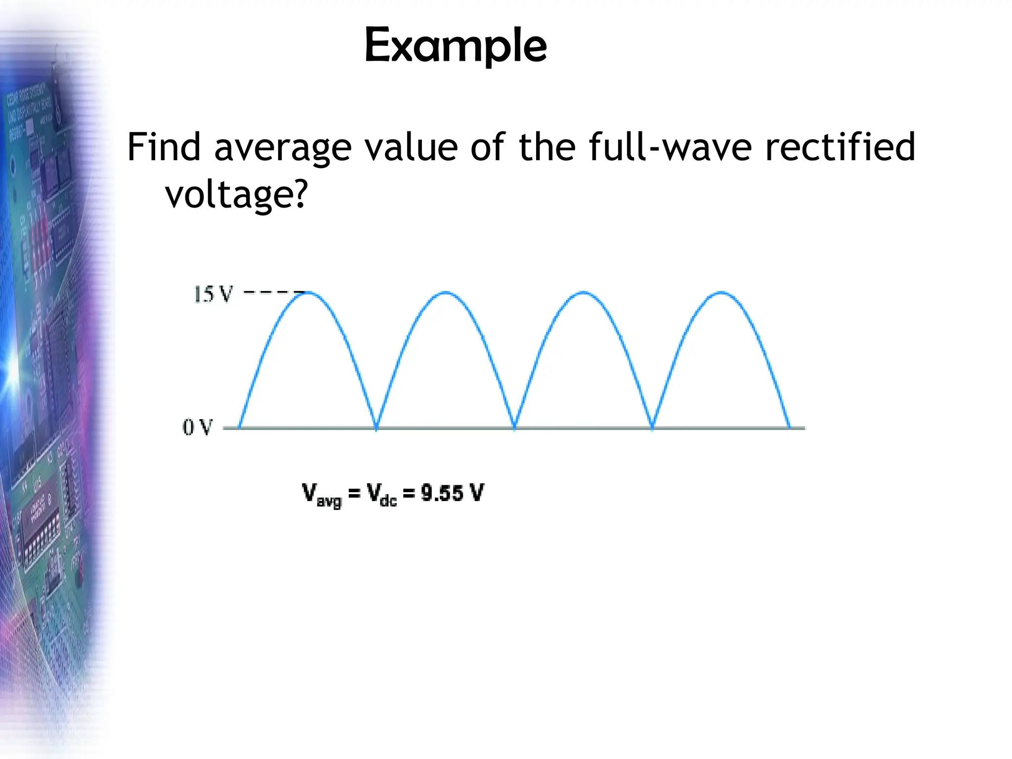
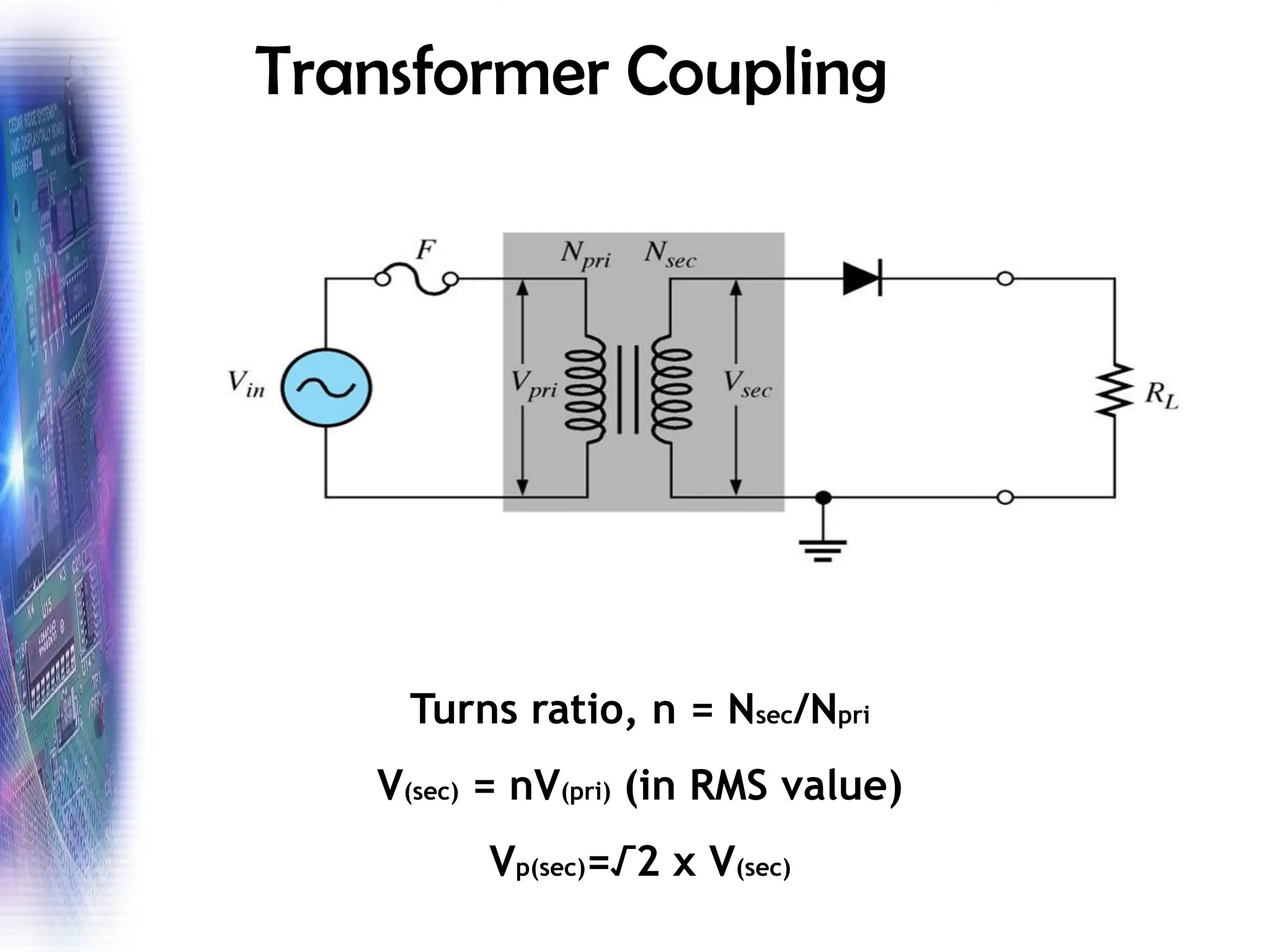
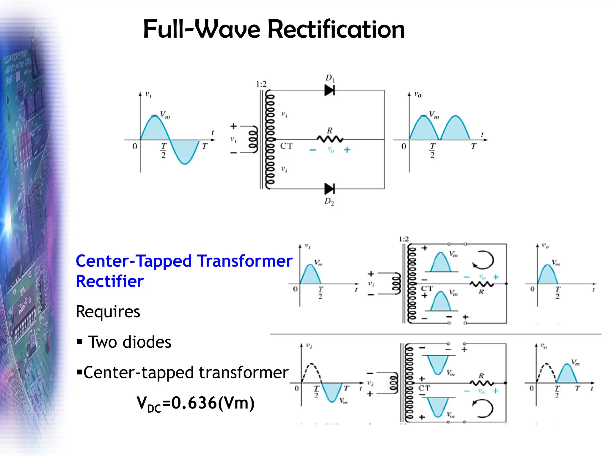
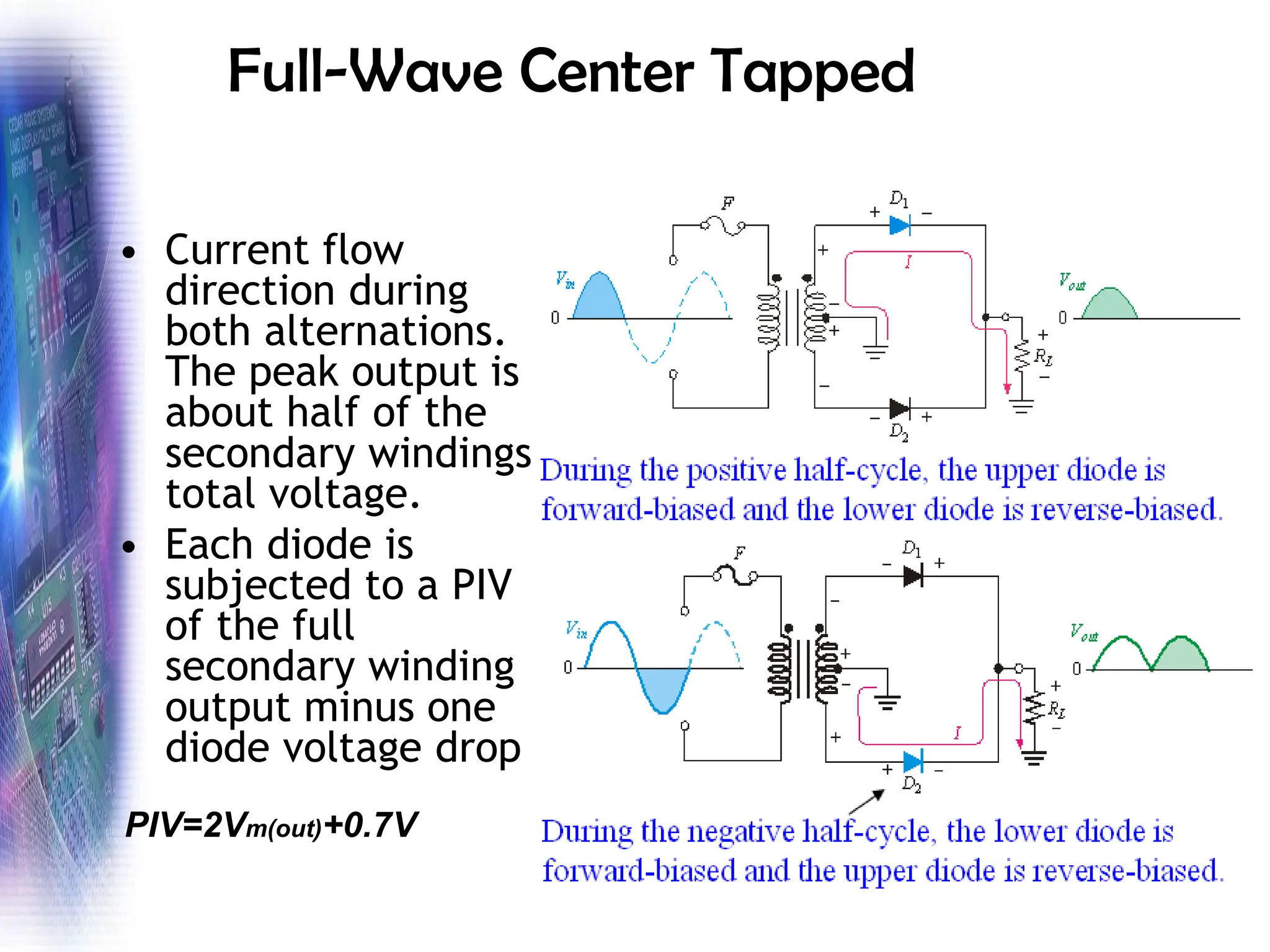
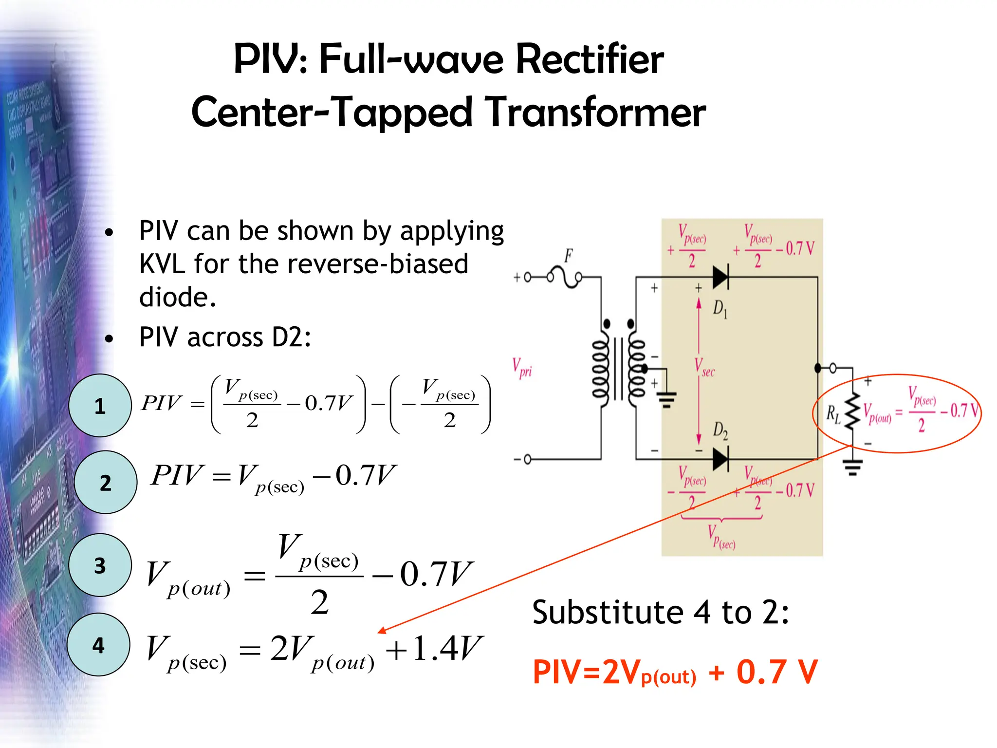
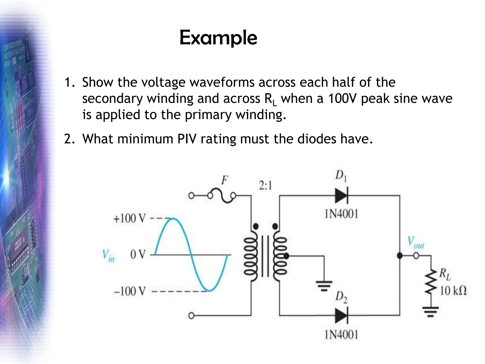
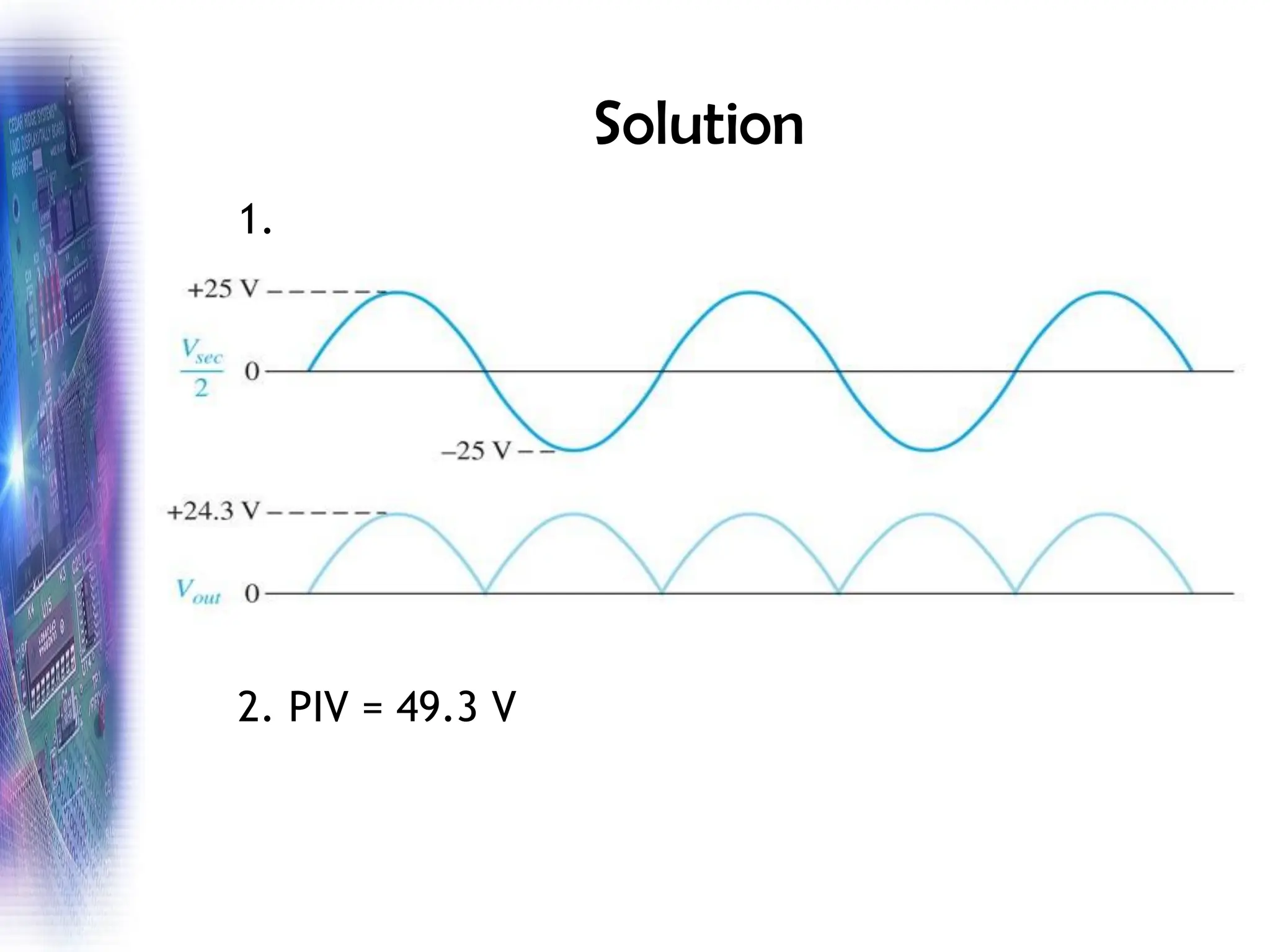
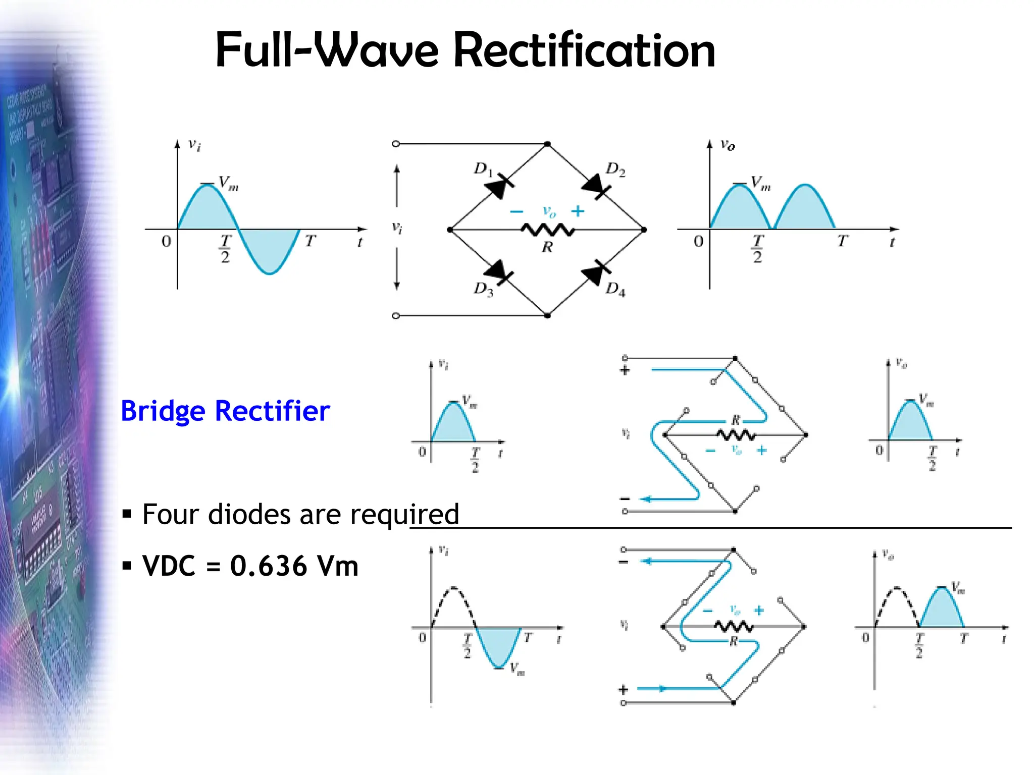
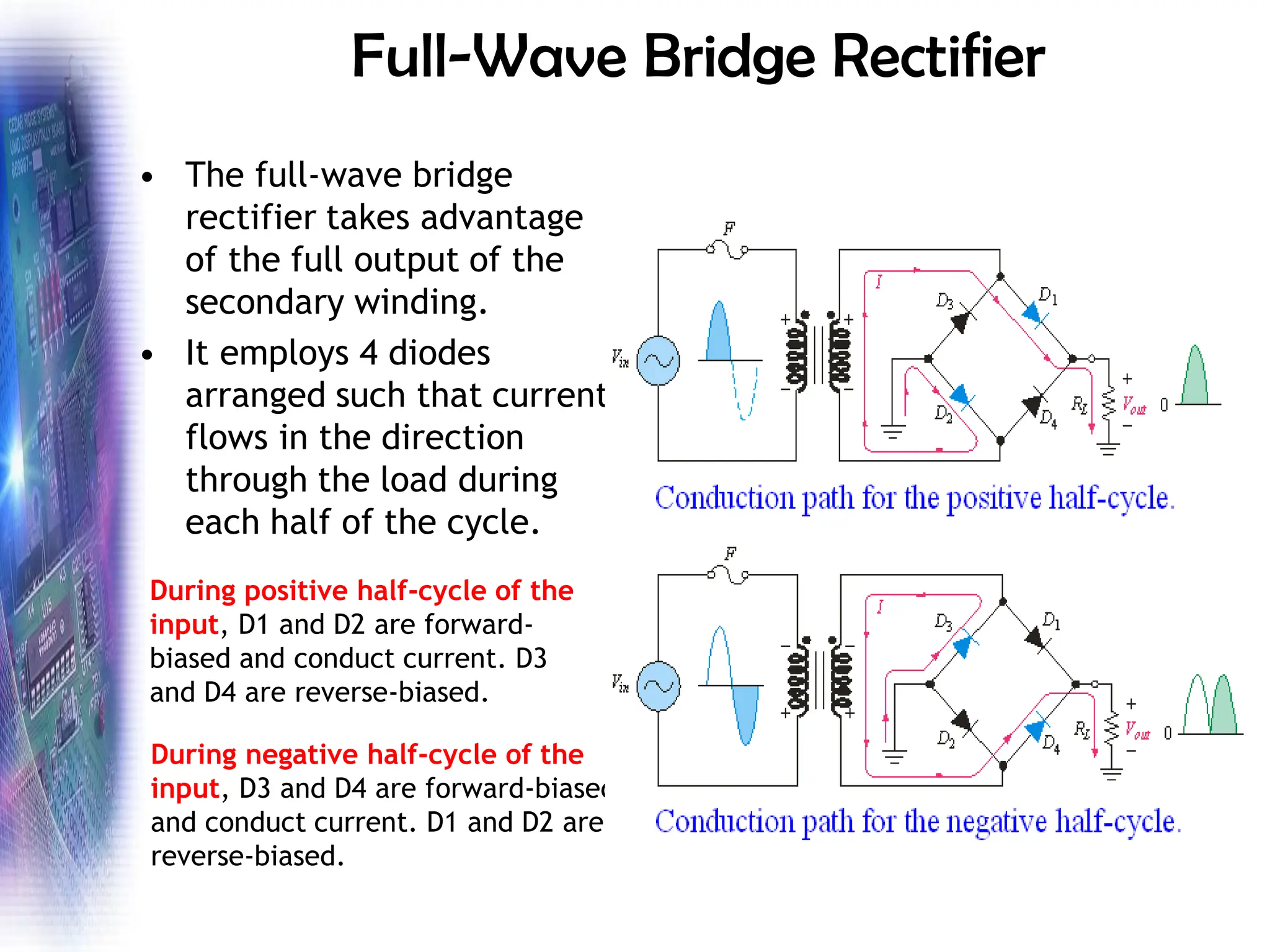
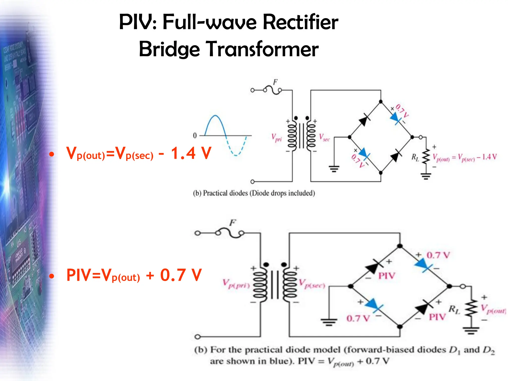
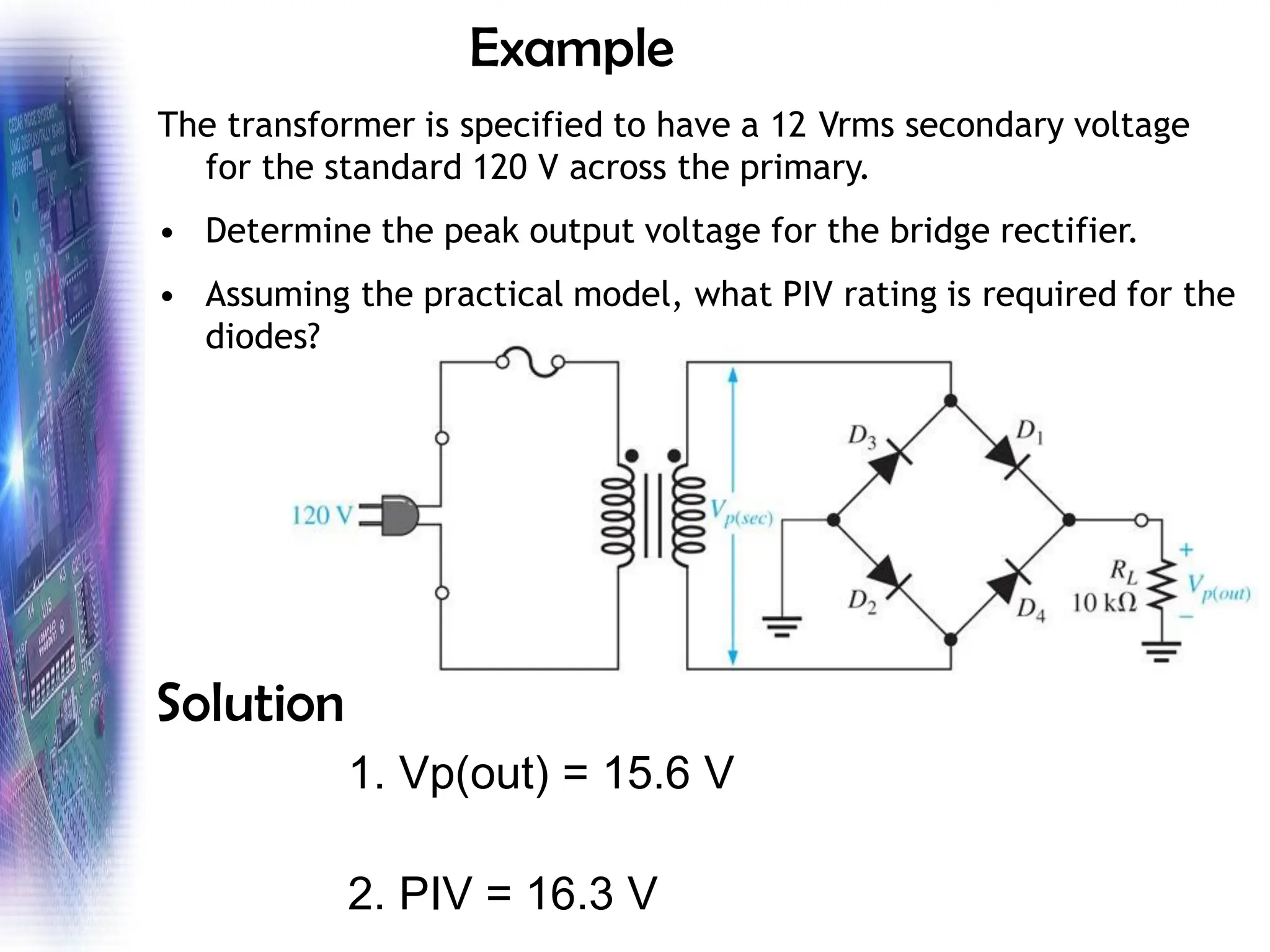
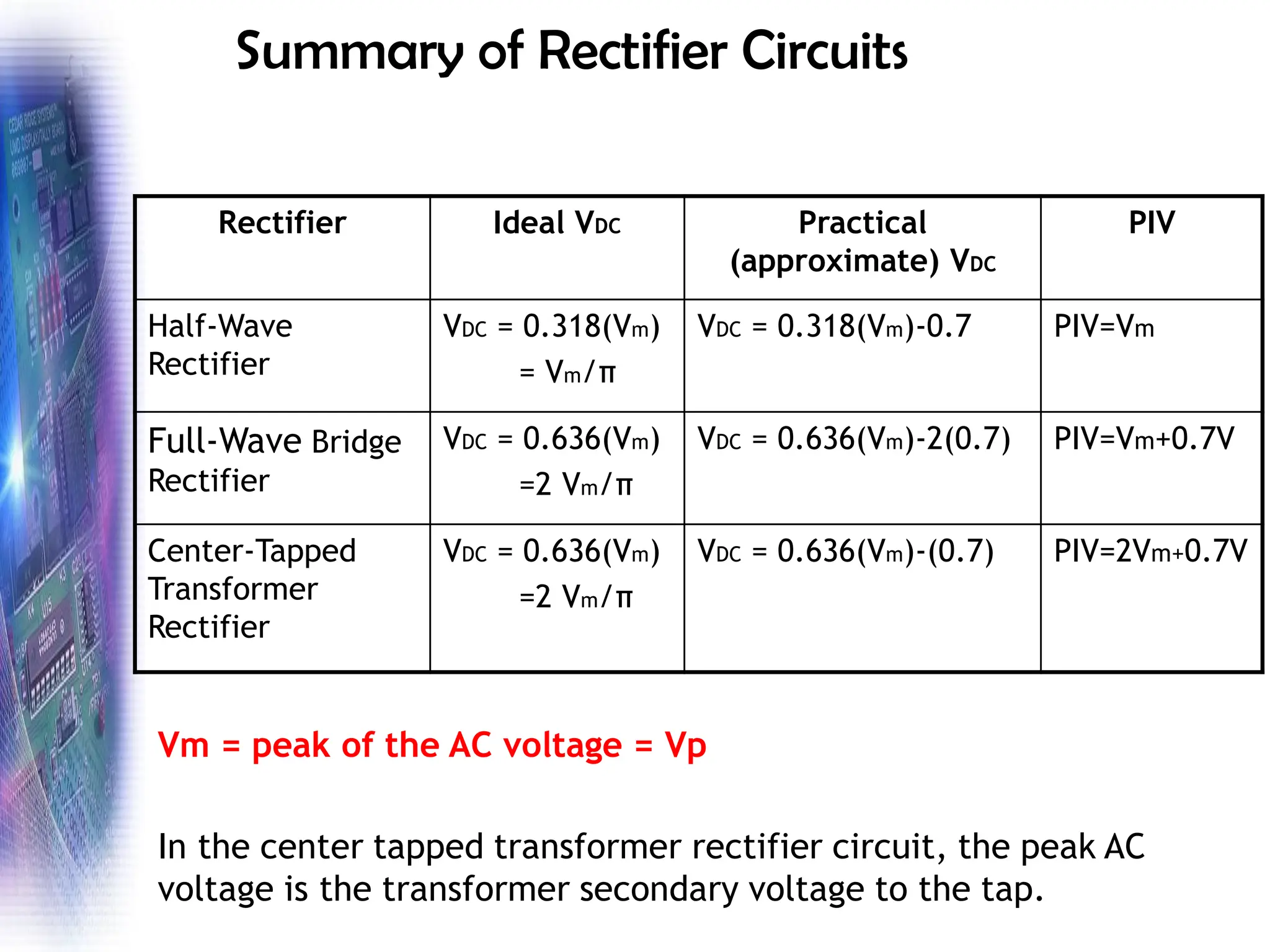
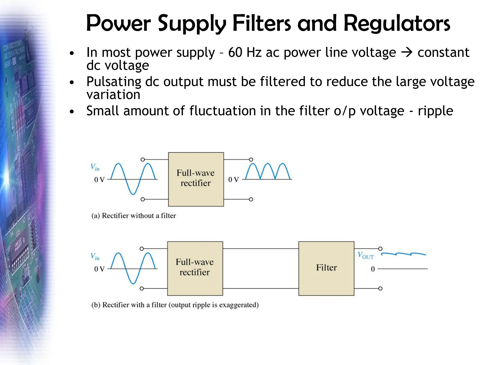
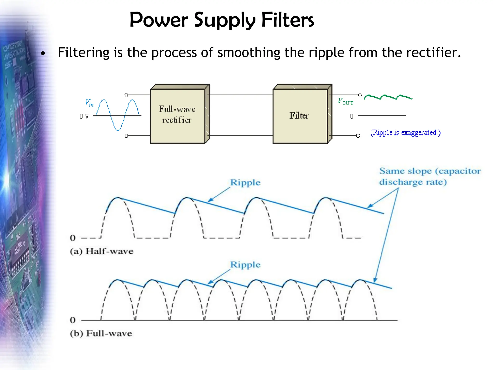
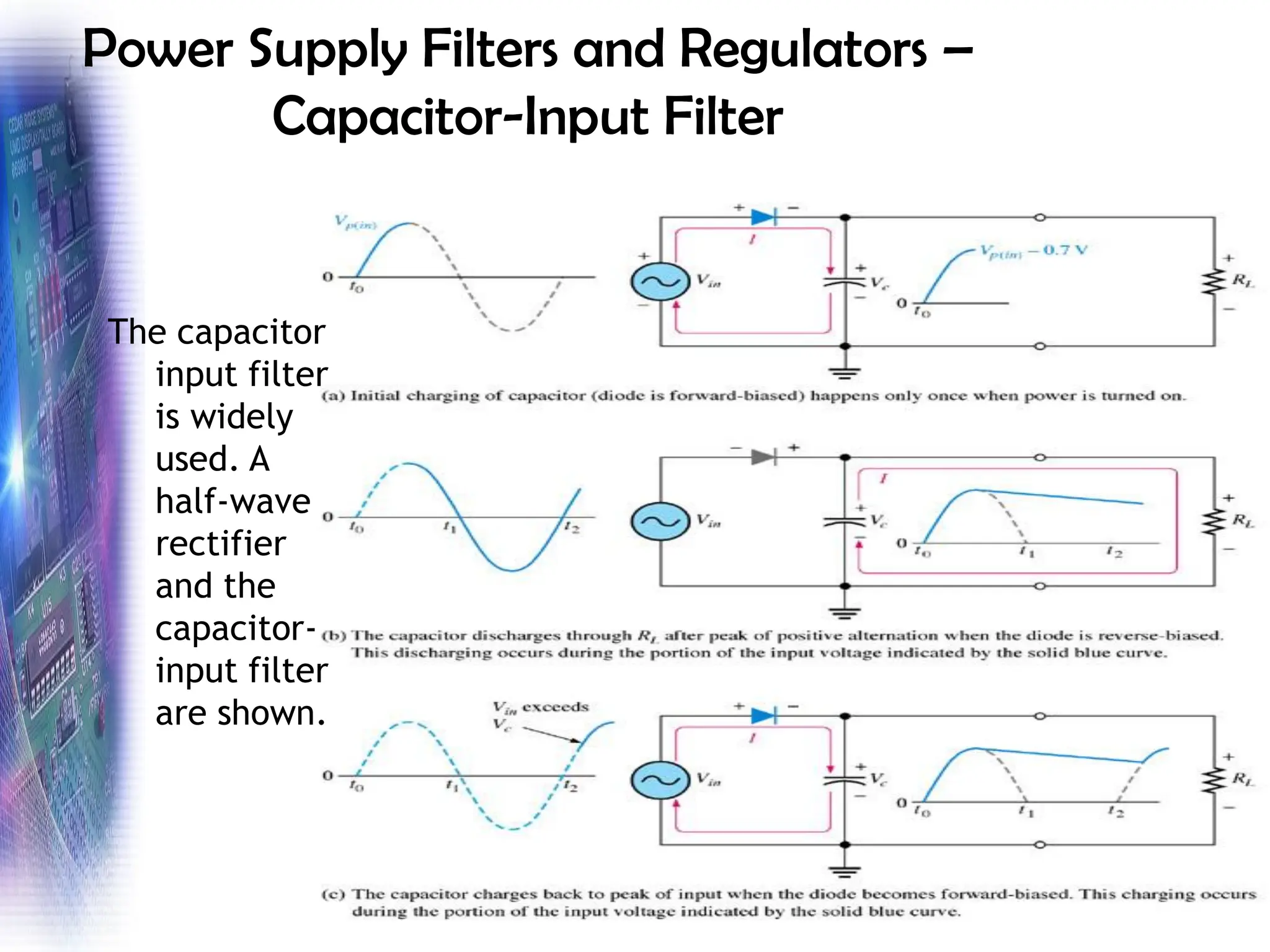
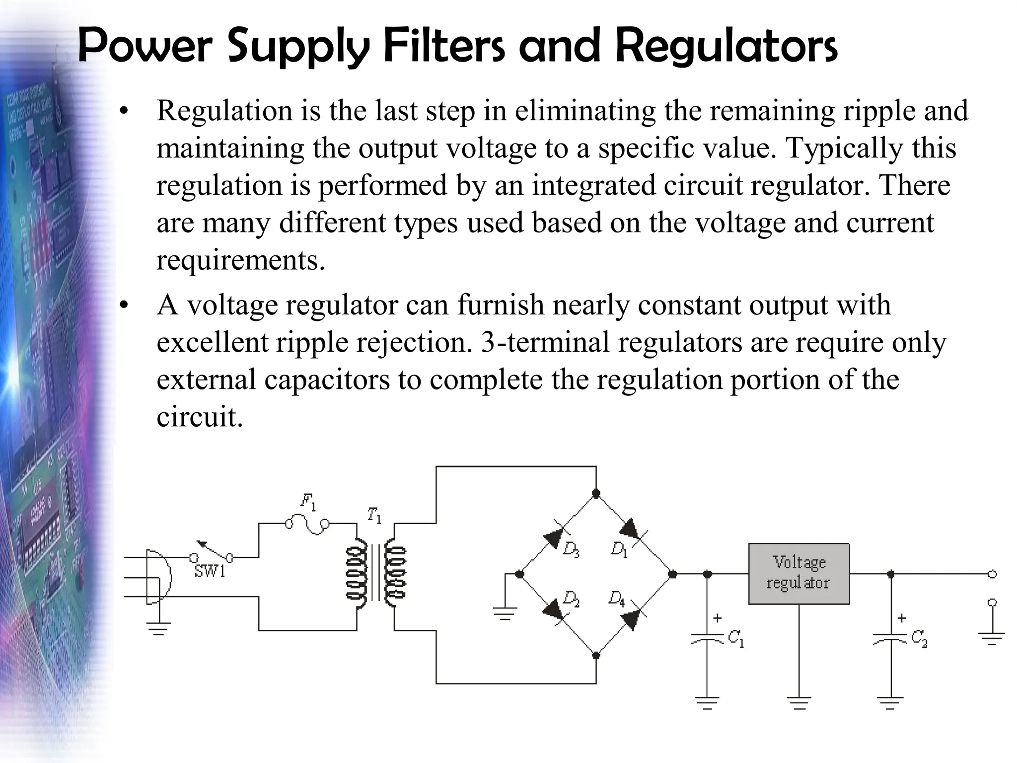
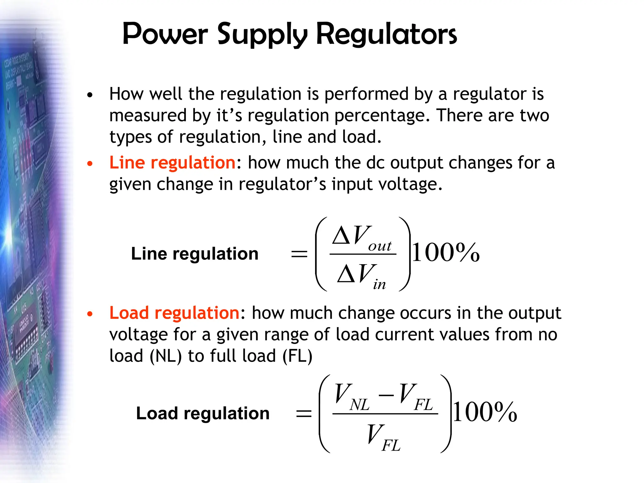
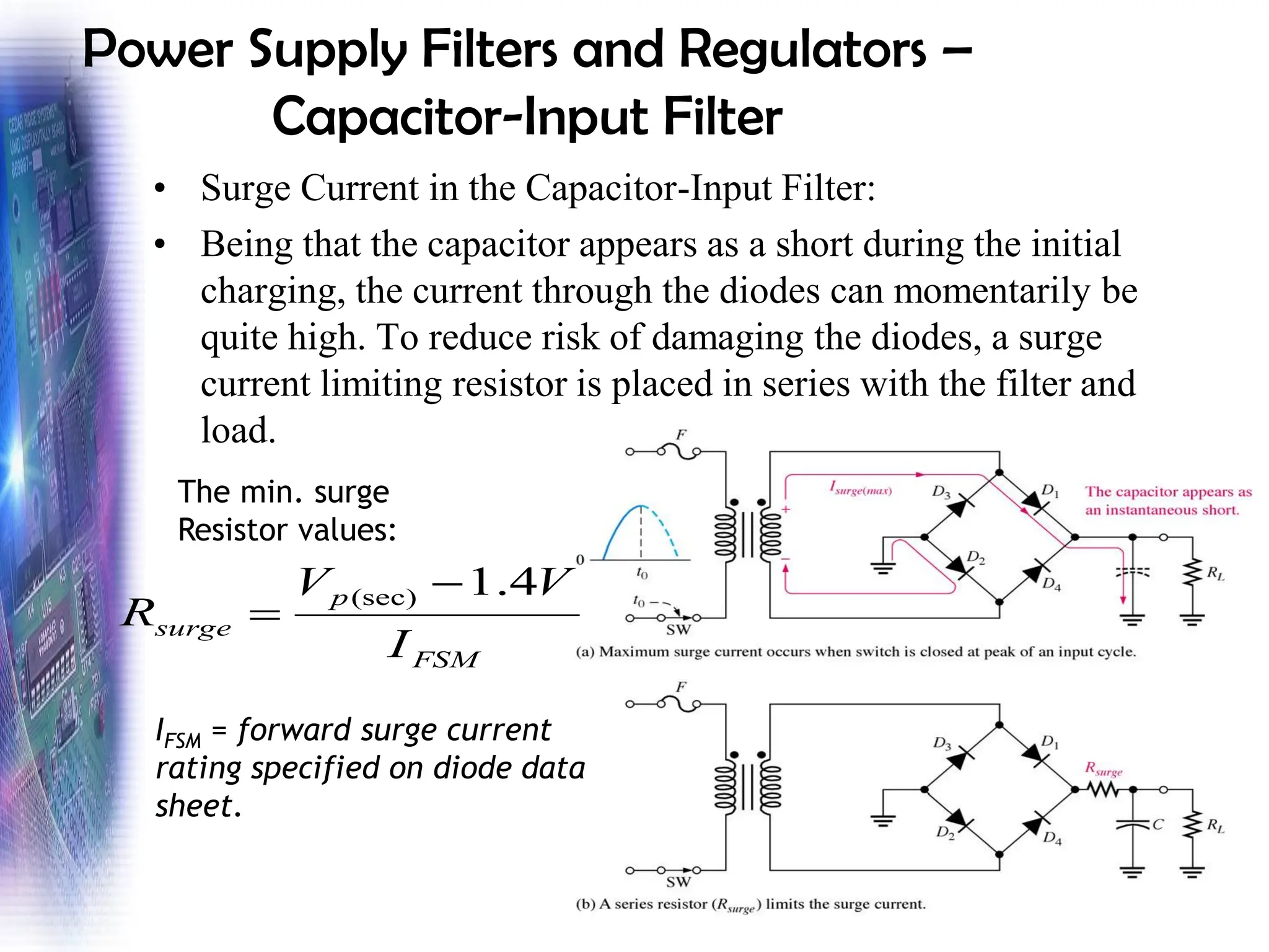
This document provides an overview of diode applications and circuit analysis techniques. It discusses load line analysis and how it is used to determine the operating point of a diode circuit. It also covers rectification circuits including half-wave and full-wave rectifiers using a center-tapped transformer or bridge configuration. The document examines peak inverse voltage ratings, filter circuits to reduce ripple voltage from rectifiers, and voltage regulators. Examples are provided to illustrate key concepts like load line analysis, rectifier output voltage calculations, and determining minimum diode ratings.

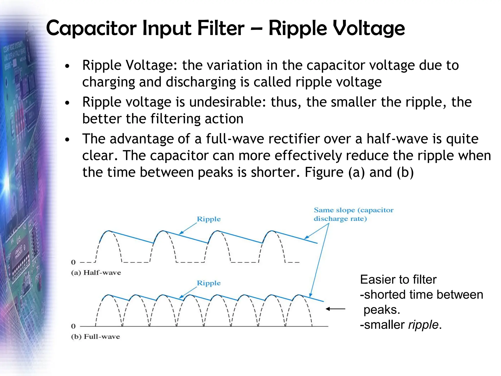
![Capacitor Input Filter – Ripple Voltage
DC
pp
r
V
V
r
)
(
=
Ripple factor: indication of the effectiveness of the filter
Vr(pp) = peak to peak ripple voltage;
VDC = VAVG = average value of filter’s
output voltage
•Lower ripple factor → better filter [can be lowered by
increasing the value of filter capacitor or increasing the load
resistance]
[half-wave rectifier]
•For the full-wave
rectifier:
)
(
)
(
)
(
2
1
1
1
rect
p
L
AVG
DC
rect
p
L
pp
r
V
C
fR
V
V
V
C
fR
V
−
=
=
Vp(rect) = unfiltered
peak](https://image.slidesharecdn.com/chapter2-240210213431-04cf0257/75/DIODE-APPLICATIONS-pdf-40-2048.jpg)